 | –≠–ª–µ–∫—Ç—Ä–æ–Ω–Ω—ã–π –∫–æ–º–ø–æ–Ω–µ–Ω—Ç: EL7560CM | –°–∫–∞—á–∞—Ç—å:  PDF PDF  ZIP ZIP |

1
Æ
FN7294
CAUTION: These devices are sensitive to electrostatic discharge; follow proper IC Handling Procedures.
1-888-INTERSIL or 321-724-7143
|
Intersil (and design) is a registered trademark of Intersil Americas Inc.
Copyright © Intersil Americas Inc. 2003. All Rights Reserved. Elantec is a registered trademark of Elantec Semiconductor, Inc.
All other trademarks mentioned are the property of their respective owners.
EL7560
Programmable CPU Power Supply Unit
The EL7560 is the simplest, most cost
effective method for powering modern
high power CPUs which require a user
adjustable output voltage. Although it is particularly designed
to function with next generation CPUs, its simple design can
provide low cost solutions for any 5V to 3V application.
The circuit uses on chip resistorless current sensing for high
efficiency, stable current mode control. An on chip
temperature sensor resets the OT pin. The OT pin can be
tied directly to the OUTEN pin for automatic overtemperature
shutdown. The user can adjust the oscillator frequency as
well as the slope compensation.
The output voltage is adjustable using a 4-bit parallel
interface. A power OK signal "PWRGD' pulls high when the
FB pin is within -7% of the programmed value.
Pinout
EL7560
(28-PIN SOIC)
TOP VIEW
Features
∑ 3.3V @ 12.4amps continuous
∑ Internal FETs
∑ >90% efficiency
∑ Synchronous switching
∑ 4-bit digitally adjustable output voltage
∑ User adjustable slope compensation
∑ Internal soft start
∑ Over temperature indicator
∑ Low current sleep mode
∑ Low parts count
∑ Pulse by pulse current limiting
∑ High efficiency at light load
∑ Operates up to 1MHz
∑ 1% output accuracy
∑ Sync function
∑ Power good signal
Applications
∑ PC motherboards
∑ Local high power CPU supplies
1
2
3
4
16
15
14
13
5
6
7
12
11
9
8
10
20
19
18
17
24
23
22
21
28
27
26
25
FB
CP-
CREF
CP+
CSLOPE
C2V
COSC
VSS
VDD
VHI
VIN
LX
VSSP
LX
VIN
LX
VSSP
LX
VSSP
LX
VID0
TEST
VID1
PWRGD
VID2
OT
VID3
OUTEN
+10V
D2
D1
R1
100
C7
+5V
4mF
C10
30
1µF
C11
68p
D3
R3
1K
2.5µH
L1
VOUT
.1µF
C6
4.7µF
C8
5V
R2
10K
+2V - 3.5V
1µF
C5
PGND
L2
1.5µH
5V
C1
OUTPUT
VOLTAGE*
SELECT
C9
2mF
.1µF
C4
220p
ACND
10
.1µF
* See VID Table on page 3
Note:
∑ AGND and PGND should be connected at C10
∑ D3 is 1.235V reference.
Ordering Information
PART
NUMBER
TEMP. RANGE
PACKAGE
PKG. NO.
EL7560CM
-40∞C to +85∞C
28-Pin SOIC
MDP0027
Data Sheet
August 21, 1998
OBS
OLE
TE P
ROD
UCT
NO R
ECO
MME
NDE
D RE
PLA
CEM
ENT
cont
act o
ur T
echn
ical
Sup
port
Cen
ter a
t
1-88
8-IN
TER
SIL
or w
ww.i
nter
sil.c
om/t
sc

2
NOTE:
1. The oscillator and voltage doubler operate normally when V
DD
exceeds V
DD-ON
threshold, independent of the OUTEN logic level.
Absolute Maximum Ratings
(T
A
= 25∞C)
Supply (V
IN
, V
DD
) . . . . . . . . . . . . . . . . . . . . . . . . . . . . . . . . . . . 5.5V
Output Pins . . . . . . . . . . . . . . . -0.3V below GND, +0.3V above V
DD
Instantaneous Peak Output Current . . . . . . . . . . . . . . . . . . . . . .16A
Storage Temperature Range . . . . . . . . . . . . . . . . . .-65∞C to +150∞C
Ambient Operating Temperature . . . . . . . . . . . . . . . . -40∞C to +85∞C
Operating Junction Temperature . . . . . . . . . . . . . . . . . . . . . . . 135∞C
Power Dissipation . . . . . . . . . . . . . . . . . . . . . . . . . . . . . . . . . . . . 3W
CAUTION: Stresses above those listed in "Absolute Maximum Ratings" may cause permanent damage to the device. This is a stress only rating and operation of the
device at these or any other conditions above those indicated in the operational sections of this specification is not implied.
IMPORTANT NOTE: All parameters having Min/Max specifications are guaranteed. Typical values are for information purposes only. Unless otherwise noted, all tests
are at the specified temperature and are pulsed tests, therefore: T
J
= T
C
= T
A
DC Electrical Specifications
V
DD
= V
IN
= 5V, C
OSC
= 1nF, C
SLOPE
= 68pF, T
A
= 25∞C, unless otherwise specified (Note 1)
PARAMETER
DESCRIPTION
CONDITION
MIN
TYP
MAX
UNITS
V
2X
Voltage Doubler Output
V
DD
=5V, I
LOAD
=20mA
8.0
9
9.5
V
DAC
LSB
DAC Resolution
0.095
0.105
V
F
OSC
Oscillator Initial Accuracy
105
120
135
kHz
F
OSCTC
Oscillator Tempco
0∞C<T
A
<125∞C
±0.1
%/∞C
V
RAMP
Oscillator Ramp Amplitude
1.2
V
M
SS
Soft Start Slope
F
OSC
=500kHz
0.3
V/msec
I
VID
VID Pull Up Current
VID = 0V
9
13
18
µA
I
CSLOPE
C
SLOPE
Charging Current
32
40
48
µA
I
DD
Supply Current
OUTEN=4V F
OSC
=120kHz
25
35
mA
I
DDOFF
Stdby Current
OUTEN=0V
3
5
mA
R
DSON
Composite FET Resistance
18
25
m
R
DSONTC
R
DSON
Tempco
0.1
m
/∞C
V
OUT
Output Initial Acurracy
VID=0111
2.765
2.8
2.835
V
V
RANGE
Output Voltage Range
VID=1110 to 0000
2.065
3.535
V
I
LMAX
Maximum current
V
OUT
=0
14.0
amps
V
OUT-TC
Output Tempco
0∞C<T
A
<70∞C
±1
%
V
OUT-LINE
Output Line Regulation
V
OUT
=2.8, 4.5V
DD
<5.5, V
DD
=V
IN
-1
1
%
V
OUT-LOAD
Output Load Regulation
0.3A<I
LOAD
<12.4A
-1
1
%
V
OUT-TOT
Output Total Variation
-2
2
%
OT
OFF
Over Temperature Threshold
135
∞C
OT
HYS
Over Temperature Hysteresis
50
∞C
V
PWRGD
Power Good Threshold with Respect to
Desired OutputVoltage
VID=0111
-9
-7
-5
%
V
DD-ON
Minimum V
DD
form Startup
4
V
V
DD-OFF
Maximum V
DD
for Shutdown
3.75
V
EL7560

3
Voltage Identification Codes
P6 PINS
V
ID0
V
DC
V
ID3
V
ID2
V
ID1
1
1
1
1
0, No CPU
1
1
1
0
2.1
1
1
0
1
2.2
1
1
0
0
2.3
1
0
1
1
2.4
1
0
1
0
2.5
1
0
0
1
2.6
1
0
0
0
2.7
0
1
1
1
2.8
0
1
1
0
2.9
0
1
0
1
3.0
0
1
0
0
3.1
0
0
1
1
3.2
0
0
1
0
3.3
0
0
0
1
3.4
0
0
0
0
3.5
EL7560

4
NOTE:
1. The oscillator and voltage doubler operate normally when V
DD
exceeds V
DD-ON
threshold, independent of the OUTEN logic level.
EL7560 Pin Descriptions
PIN
NUMBER
NAME
DESCRIPTION
1
C
P
-
Negative input for the charge pump bootstrap capacitor. (Note 1)
2
C
P
+
Positive input for the charge pump bootstrap capacitor. (Note 1)
3
C2V
Voltage doubler output. Pin requires at least a 1µF capacitor to GND. (Note 1)
4
V
SS
Ground return for the control circuitry.
5
V
HI
Positive supply for the high side driver. This pin is bootstrapped from the LX pin with a 0.1µF capacitor.
6
LX
Common connection between the two large internal FETs. External inductor connection.
7
LX
Same as pin 6.
8
LX
Same as pin 6.
9
LX
Same as pin 6.
10
LX
Same as pin 6.
11
TEST
This is test pin and must remain grounded at all times
12
PWRGD
Pin pulls high when the FB pin is within - 7%(typ) of its programmed value.
13
OT
Overtemperature indicator. Pulls low when the die temperature exceeds 135∞C. Pin has 10mA pull-up.
14
OT
A logic high on OUTEN enables the regulator (Note 1)
15
VID3
Bit 3(MSB) of the output voltage select DAC.
16
VID2
Bit 2 of the output voltage select DAC.
17
VID1
Bit 1 of the output voltage select DAC.
18
VID0
Bit 0(LSB) of the output voltage select DAC.
19
V
SSP
Ground return to the buck regulator.
20
V
SSP
Same as pin 19.
21
V
IN
Positive power supply input to the buck regulator.
22
V
SSP
Same as pin 19.
23
V
IN
Same as pin 21.
24
V
DD
Pin supplies power to the internal control circuitry.
25
C
OSC
Oscillator timing capacitor. Oscillator Frequency is approximately: F
OSC
(Hz)=0.0001/C
OSC
(F). The duty cycle is
approximately 5%. (Note 1)
26
C
SLOPE
Slope compensation capacitor.
27
C
REF
External reference input pin.
28
FB
Voltage feedback pin for the buck regulator.
EL7560
5
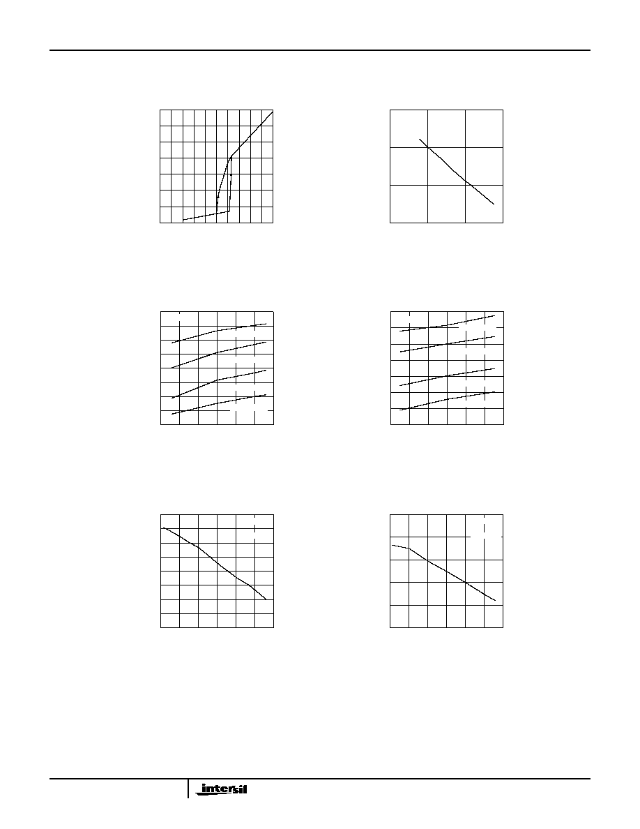
Typical Performance Curves
I
DD
vs V
DD
5
35
30
25
20
15
10
0
I
DD
(m
A
)
V
DD
(V)
1
6
3
2
4
5
Oscillator Frequency vs C
OSC
100
10000
1000
10
Freq
uency (kHz)
C
OSC
(pF)
10
10000
100
1000
ILine Regulation (VID3:0=0000)
3.475
3.545
3.535
3.525
3.515
3.505
3.495
3.485
3.465
V
OU
T
(V
)
V
IN
(V)
4.4
5.0
5.6
4.6
4.8
5.2
5.4
I
OUT
= 0.3A
T
A
=25∞C
Load Regulation (VID3:0=0000)
3.47
3.54
3.53
3.52
3.51
3.50
3.49
3.48
3.46
V
OU
T
(V
)
I
OUT
(A)
0
6
12
2
4
8
10
V
IN
=5V
T
A
=25∞C
Line Regulation (VID3:0=1101)
2.17
2.23
2.22
2.21
2.20
2.19
2.18
2.16
V
OUT
(V
)
V
IN
(V)
4.4
5.0
5.6
4.6
4.8
5.2
5.4
T
A
=25∞C
I
OUT
= 4A
I
OUT
= 8A
I
OUT
= 11A
I
OUT
= 0.3A
I
OUT
= 4A
I
OUT
= 8A
I
OUT
= 11A
Load Regulation (VID3:0=1101)
2.17
2.25
2.23
2.21
2.19
2.15
V
OUT
(V
)
I
OUT
(A)
0
6
12
2
4
8
10
V
IN
=5V
T
A
=25∞C
EL7560