 | –≠–ª–µ–∫—Ç—Ä–æ–Ω–Ω—ã–π –∫–æ–º–ø–æ–Ω–µ–Ω—Ç: EL7562 | –°–∫–∞—á–∞—Ç—å:  PDF PDF  ZIP ZIP |
1
Æ
FN7295
CAUTION: These devices are sensitive to electrostatic discharge; follow proper IC Handling Procedures.
1-888-INTERSIL or 321-724-7143
|
Intersil (and design) is a registered trademark of Intersil Americas Inc.
Copyright © Intersil Americas Inc. 2004. All Rights Reserved. Elantec is a registered trademark of Elantec Semiconductor, Inc.
All other trademarks mentioned are the property of their respective owners.
EL7562
Monolithic 2Amp DC-DC Step-Down
Regulator
The EL7562 is an integrated,
synchronous step-down regulator with
output voltage adjustable from 1.0V to
3.8V. It is capable of delivering 2A continuous current at up
to 95% efficiency. The EL7562 operates at a constant
frequency pulse width modulation (PWM) mode, making
external synchronization possible. Patented on-chip
resistorless current sensing enables current mode control,
which provides cycle-by-cycle current limiting, over-current
protection, and excellent step load response. The EL7562 is
available in a fused-lead 16-pin QSOP package. With proper
external components, the whole converter fits into a less
than 0.5 in
2
area. The minimal external components and
small size make this EL7562 ideal for desktop and portable
applications.
The EL7562 is specified for operation over the 0∞C to +70∞C
temperature range.
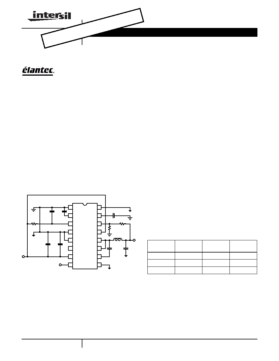
Pinout
EL7562
(16-PIN QSOP)
TOP VIEW
Features
∑ Integrated synchronous MOSFETs and current mode
controller
∑ 2A continuous output current
∑ Up to 95% efficiency
∑ 3.3V or 5V nominal input voltage
∑ Adjustable output from 1V to 3.8V
∑ Cycle-by-cycle current limit
∑ Precision reference
∑ ±0.5% load and line regulation
∑ Adjustable switching frequency to 1MHz
∑ Oscillator synchronization possible
∑ Internal soft-start
∑ Over-temperature protection
∑ Under-voltage lockout
∑ 16-pin QSOP package
Applications
∑ DSP, CPU core and IO supplies
∑ Logic/Bus supplies
∑ Portable equipment
∑ DC-DC converter modules
∑ GTL + Bus power supply
Please refer to page 4 for 3.3V input Application Diagram
Manufactured under U.S. Patent No. 57,323,974
1
2
3
4
16
15
14
13
5
6
7
12
11
10
8
9
SGND
COSC
VDD
PGND
PGND
VIN
VIN
EN
PGND
VREF
FB
VDRV
LX
LX
VHI
PGND
C
4
270pF
C
3
0.1µF
C
2
0.1µF
C
1
100µF
R
3
39
V
IN
(4.5V- 5.5V)
C
6
0.1µF
C
7
100µF
R
2
2.37k
R
1
1k
C
5
0.1µF
V
O
(3.3V,
2A)
Ordering Information
PART
NUMBER
PACKAGE
TAPE & REEL
PKG. DWG. #
EL7562CU
16-Pin QSOP
-
MDP0040
EL7562CU-T7
16-Pin QSOP
7"
MDP0040
EL7562CU-T13 16-Pin QSOP
13"
MDP0040
Data Sheet
April 30, 2004
NOT
REC
OMM
END
ED F
OR N
EW
DES
IGN
S
SEE
EL7
532
2
Absolute Maximum Ratings
(T
A
= 25∞C)
Supply Voltage between V
IN
or V
DD
and GND . . . . . . . . . . . . +6.5V
V
LX
Voltage . . . . . . . . . . . . . . . . . . . . . . . . . . . . . . . . . . . . V
IN
+0.3V
Input Voltage . . . . . . . . . . . . . . . . . . . . . . . . GND -0.3V, V
DD
+0.3V
V
HI
Voltage . . . . . . . . . . . . . . . . . . . . . . . . . . . GND -0.3V, V
LX
+6V
Storage Temperature . . . . . . . . . . . . . . . . . . . . . . . .-65∞C to +150∞C
Operating Ambient Temperature . . . . . . . . . . . . . . . . . 0∞C to +70∞C
Operating Junction Temperature . . . . . . . . . . . . . . . . . . . . . . +135∞C
CAUTION: Stresses above those listed in "Absolute Maximum Ratings" may cause permanent damage to the device. This is a stress only rating and operation of the
device at these or any other conditions above those indicated in the operational sections of this specification is not implied.
IMPORTANT NOTE: All parameters having Min/Max specifications are guaranteed. Typical values are for information purposes only. Unless otherwise noted, all tests
are at the specified temperature and are pulsed tests, therefore: T
J
= T
C
= T
A
DC Electrical Specifications
V
DD
= V
IN
= 5V, T
A
= T
J
= 25∞C, C
OSC
= 270pF, unless otherwise specified.
PARAMETER
DESCRIPTION
CONDITIONS
MIN
TYP
MAX
UNIT
V
REF
Reference Accuracy
1.24
1.26
1.28
V
V
REFTC
Reference Temperature Coefficient
50
ppm/∞C
V
REFLOAD
Reference Load Regulation
0 < I
REF
< 50µA
-1
%
V
RAMP
Oscillator Ramp Amplitude
1.15
V
I
OSC_CHG
Oscillator Charge Current
0.1V < V
OSC
< 1.25V
200
µA
I
OSC_DIS
Oscillator Discharge Current
0.1V < V
OSC
< 1.25V
8
mA
I
VDD
+V
DRV
V
DD
+V
DRV
Supply Current
V
EN
= 4V, F
OSC
= 120kHz
2
6.5
mA
I
VDD_OFF
V
DD
Standby Current
EN = 0
1
1.5
mA
V
DD_OFF
V
DD
for Shutdown
2.5
2.7
V
V
DD_ON
V
DD
for Startup
2.6
3
V
T
OT
Over-temperature Threshold
135
∞C
T
HYS
Over-temperature Hysteresis
20
∞C
I
LEAK
Internal FET Leakage Current
EN = 0, L
X
= 5V (low FET), L
X
= 0V (high
FET)
20
µA
I
LMAX
Peak Current Limit
3
A
R
DSON
FET On Resistance
Wafer level test only
60
120
m
R
DSONTC
R
DSON
Tempco
0.2
m
/∞C
V
FB
Output Initial Accuracy
I
LOAD
= 0A
0.970
0.985
1.000
V
V
FB_LINE
Output Line Regulation
V
IN
= 5V,
V
IN
= 10%, I
LOAD
= 0A
0.5
%
V
FB_LOAD
Output Load Regulation
0.1A < I
LOAD
< 1A
0.5
%
V
FB_TC
Output Temperature Stability
-40∞C < T
A
< 85∞C, I
LOAD
= 0.5A
±1
%
I
FB
Feedback Input Pull Up Current
V
FB
= 0V
100
200
nA
V
EN_HI
EN Input High Level
(Note)
4
V
V
EN_LO
EN Input Low Level
1
V
I
EN
Enable Pull Up Current
V
EN
= 0
-4
-2.5
µA
NOTE: V
EN_HI
is typically 2/3 of V
DD
. For V
DD
= 3.3V, V
EN_HI
is 2.2V typical.
3
Closed-Loop AC Electrical Specifications
V
S
= V
IN
= 5V, T
A
= T
J
= 25∞C, C
OSC
= 270pF, unless otherwise specified.
PARAMETER
DESCRIPTION
CONDITIONS
MIN
TYP
MAX
UNIT
F
OSC
Oscillator Initial Accuracy
493
580
667
kHz
t
SYNC
Minimum Oscillator Sync Width
25
ns
M
SS
Soft-start Slope
0.5
V/ms
t
BRM
FET Break Before Make Delay
15
ns
t
LEB
High Side FET Minimum On Time
150
ns
D
MAX
Maximum Duty Cycle
95
%
Pin Descriptions
PIN
NUMBER
PIN NAME
PIN FUNCTION
1
SGND
Control circuit negative supply
2
COSC
Oscillator timing capacitor; F
OSC
can be approximated by: F
OSC
(kHz) = 0.1843/C
OSC
, C
OSC
in µF
3
VDD
Control circuit positive supply
4
PGND
Ground return of the regulator; connected to the source of the low-side synchronous NMOS power FET
5
PGND
Ground return of the regulator; connected to the source of the low-side synchronous NMOS power FET
6
VIN
Power supply input of the regulator; connected to the drain of the high-side NMOS power FET
7
VIN
Power supply input of the regulator; connected to the drain of the high-side NMOS power FET
8
EN
Chip enable, active high; a 2µA internal pull-up current enables the device if the pin is left open
9
PGND
Ground return of the regulator
10
VHI
Positive supply of the high-side driver
11
LX
Inductor drive pin; high current digital output whose average voltage equals the regulator output voltage
12
LX
Inductor drive pin; high current digital output whose average voltage equals the regulator output voltage
13
VDRV
Positive supply of the low-side driver and input voltage for the high-side boot strap
14
FB
Voltage feedback input; connected to an external resistor divider between V
OUT
and GND; a 125nA pull-up current
forces V
OUT
to V
S
in the event that FB is floating
15
VREF
Bandgap reference bypass capacitor; typically 0.1µF to GND
16
PGND
Ground return of the regulator
4
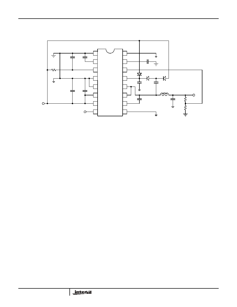
Application Diagram for 3.3V Input
1
2
3
4
16
15
14
13
5
6
7
12
11
10
8
9
SGND
COSC
VDD
PGND
PGND
VIN
VIN
EN
PGND
VREF
FB
VDRV
LX
LX
VHI
PGND
R
3
L
1
C
3
C
4
C
1
C
2
C
5
C
6
C
7
V
O
(2.5V, 2A)
V
IN
(3V-3.6V)
0.1µF
270pF
39
100µF
0.1µF
0.1µF
0.1µF
4.7µF
100µF
R
2
1.54k
R
1
1k
C
9
0.1µF
C
8
0.1µF
D
2
D
3
D
4
EL7562
(16-Pin QSOP)
5
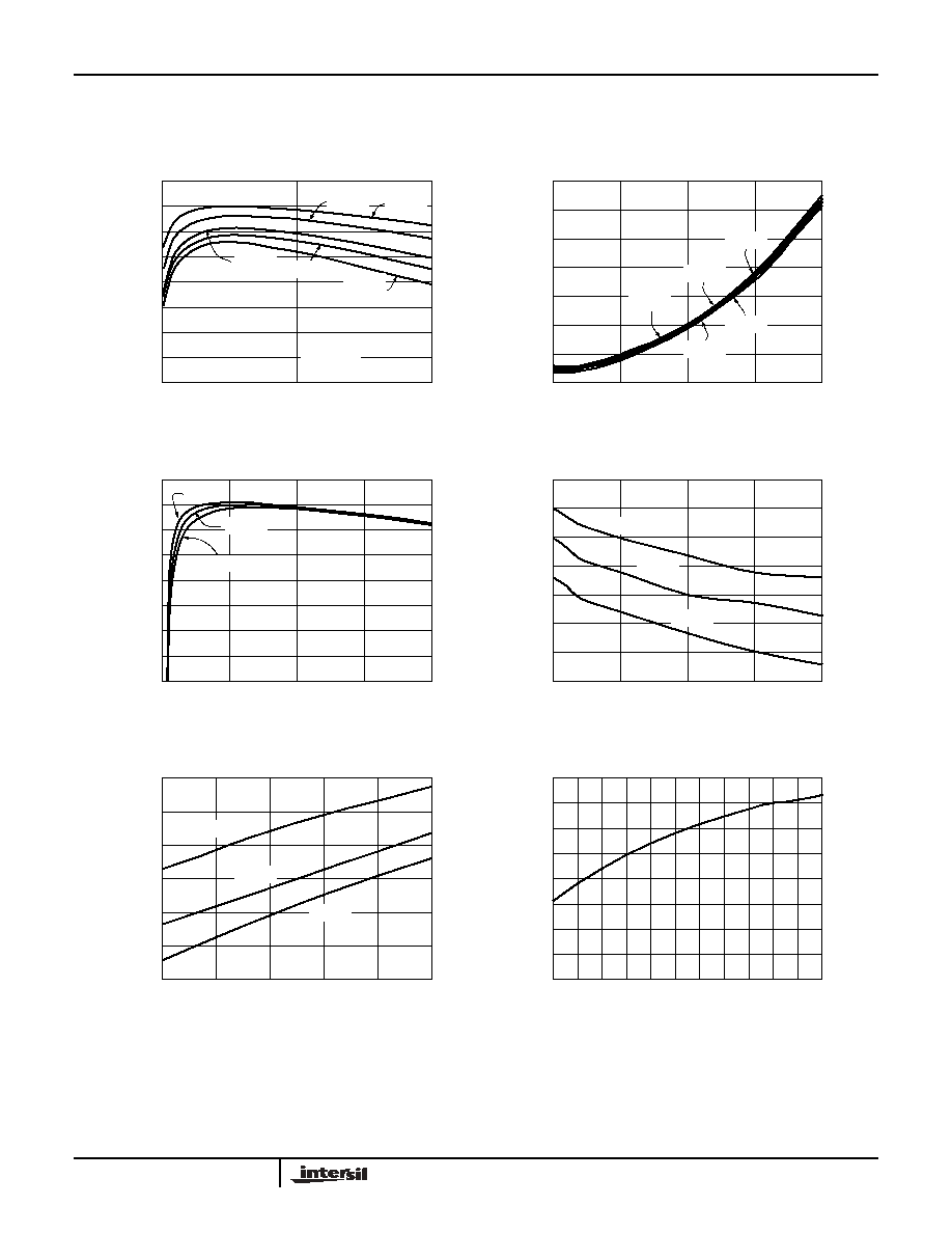
Typical Performance Curves
Efficiency vs I
O
V
IN
=5V
100
95
90
85
80
75
70
65
60
0.1
1
2
Load Current I
O
(A)
E
ffi
ci
ency (%
)
L=Coilcraft DO3316P-
V
O
=2.5
V
O
=1.8
V
O
=1.5
V
O
=1.2
V
O
=3.3
Power Loss vs I
O
V
IN
=5V
0.7
0.6
0.5
0.4
0.3
0.2
0.1
0
0
0.5
1
1.5
2
Load Current I
O
(A)
P
o
wer
Lo
ss
(W
)
Load Regulation
V
O
=3.3V
0.8
0.6
0.4
0.2
0
-0.2
-0.4
-0.6
0
0.5
1
1.5
2
Load Current I
O
(A)
Output V
o
lt
age (%)
Efficiency vs I
O
V
O
=3.3V
100
95
90
85
80
75
70
65
60
0
0.5
1
1.5
2
Load Current I
O
(A)
Effi
ci
ency (%
)
Line Regulation
V
O
=3.3V
0.6
0.4
0.2
0
-0.2
-0.4
-0.6
4.5
4.7
5.1
5.3
5.5
V
IN
(V)
V
O
(%)
V
IN
=4.5
V
IN
=5V
V
IN
=5.5
V
IN
=4.5
V
IN
=5V
V
IN
=5.5
4.9
I
O
=0.1A
I
O
=1A
I
O
=2A
Power Loss vs I
O
V
IN
=5V
0.7
0.6
0.5
0.4
0.3
0.2
0.1
0
0
0.5
1
1.5
2
Load Current I
O
(A)
P
o
wer
Lo
ss
(W
)
V
O
=2.5
V
O
=1.8
V
O
=1.5
V
O
=1.2
V
O
=3.3
F
S
=500kH
V
REF
vs Temperature
1.258
1.256
1.254
1.252
1.25
1.248
1.246
1.244
1.242
0
10
110
Temperature (∞C)
V
REF
(V)
20
30
40
50
60
70
80
90 100