 | ÐлекÑÑоннÑй компоненÑ: EL7564CM | СкаÑаÑÑ:  PDF PDF  ZIP ZIP |
Äîêóìåíòàöèÿ è îïèñàíèÿ www.docs.chipfind.ru

1
®
FN7297.3
EL7564
Monolithic 4 Amp DC/DC Step-Down
Regulator
The EL7564 is an integrated, full-featured synchronous step-
down regulator with output voltage adjustable from 1.0V to
3.8V. It is capable of delivering 4A continuous current at up
to 95% efficiency. The EL7564 operates at a constant
frequency pulse width modulation (PWM) mode, making
external synchronization possible. Patented on-chip
resistorless current sensing enables current mode control,
which provides cycle-by-cycle current limiting, over-current
protection, and excellent step load response. The EL7564
features power tracking, which makes the start-up
sequencing of multiple converters possible. A junction
temperature indicator conveniently monitors the silicon die
temperature, saving the designer time on the tedious
thermal characterization. The minimal external components
and full functionality make this EL7564 ideal for desktop and
portable applications.
The EL7564 is specified for operation over the -40°C to
+85°C temperature range.
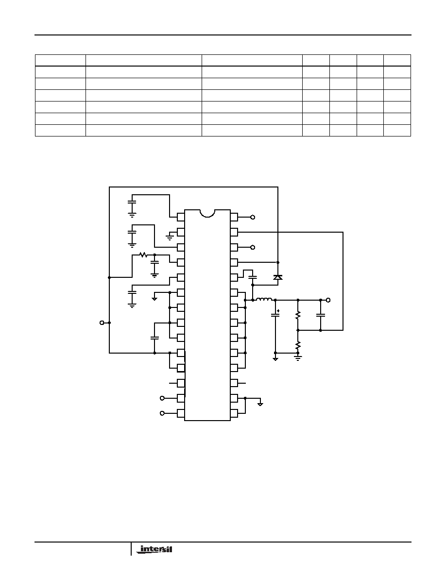
Typical Application Diagrams
EL7564
[20-PIN SO (0.300")]
TOP VIEW
Features
· Integrated synchronous MOSFETs and current mode
controller
· 4A continuous output current
· Up to 95% efficiency
· 4.5V to 5.5V input voltage
· Adjustable output from 1V to 3.8V
· Cycle-by-cycle current limit
· Precision reference
· ±0.5% load and line regulation
· Adjustable switching frequency to 1MHz
· Oscillator synchronization possible
· Internal soft start
· Over voltage protection
· Junction temperature indicator
· Over temperature protection
· Under voltage lockout
· Multiple supply start-up tracking
· Power good indicator
· 20-pin SO (0.300") package
· 28-pin HTSSOP package
· Pb-Free available (RoHS compliant)
Applications
· DSP, CPU core and IO supplies
· Logic/Bus supplies
· Portable equipment
· DC/DC converter modules
· GTL + Bus power supply
Manufactured Under U.S. Patent No. 5,7323,974
Typical Application Diagrams continued on page 3
1
2
3
4
16
15
14
13
5
6
7
12
11
9
8
10
20
19
18
17
0.1µF
390pF
0.22µF
22
2.2nF
330µF
V
IN
5V
V
OUT
3.3V, 4A
2.37k
1k
330µF
0.22µF
4.7µH
VREF
SGND
COSC
VDD
VTJ
PGND
PGND
VIN
STP
STN
EN
FB
PG
VDRV
VHI
LX
LX
PGND
PGND
PGND
100pF
C5
C4
R4
C3
C2
C1
C6
D1
L1
C7
R2
C10
R1
Data Sheet
May 9, 2005
NOT
REC
OMM
END
ED F
OR
NEW
DES
IGN
S
SEE
EL7
554
CAUTION: These devices are sensitive to electrostatic discharge; follow proper IC Handling Procedures.
1-888-INTERSIL or 1-888-352-6832
|
Intersil (and design) is a registered trademark of Intersil Americas Inc.
Copyright Intersil Americas Inc. 2003, 2005. All Rights Reserved
All other trademarks mentioned are the property of their respective owners.
2
FN7297.3
May 9, 2005
Ordering Information
PART NUMBER
PACKAGE
TAPE &
REEL
PKG. DWG.
#
EL7564CM
20-Pin SO (0.300")
-
MDP0027
EL7564CM-T13
20-Pin SO (0.300")
13"
MDP0027
EL7564CMZ
(See Note)
20-Pin SO (0.300")
(Pb-free)
-
MDP0027
EL7564CMZ-T13
(See Note)
20-Pin SO (0.300")
(Pb-free)
13"
MDP0027
EL7564CRE
28-Pin HTSSOP
-
MDP0048
EL7564CRE-T7
28-Pin HTSSOP
7"
MDP0048
EL7564CRE-T13
28-Pin HTSSOP
13"
MDP0048
EL7564CREZ
(See Note)
28-Pin HTSSOP
(Pb-free)
-
MDP0048
EL7564CREZ-T7
(See Note)
28-Pin HTSSOP
(Pb-free)
7"
MDP0048
EL7564CREZ-T13
(See Note)
28-Pin HTSSOP
(Pb-free)
13"
MDP0048
NOTE: Intersil Pb-free products employ special Pb-free material sets;
molding compounds/die attach materials and 100% matte tin plate
termination finish, which are RoHS compliant and compatible with
both SnPb and Pb-free soldering operations. Intersil Pb-free products
are MSL classified at Pb-free peak reflow temperatures that meet or
exceed the Pb-free requirements of IPC/JEDEC J STD-020.
EL7564
3
FN7297.3
May 9, 2005
Absolute Maximum Ratings
(T
A
= 25°C)
Supply Voltage between V
IN
or V
DD
and GND . . . . . . . . . . . . +6.5V
V
LX
Voltage . . . . . . . . . . . . . . . . . . . . . . . . . . . . . . . . . . . . V
IN
+0.3V
Input Voltage . . . . . . . . . . . . . . . . . . . . . . . . GND -0.3V, V
DD
+0.3V
V
HI
Voltage . . . . . . . . . . . . . . . . . . . . . . . . . . GND -0.3V, V
LX
+6.5V
Storage Temperature . . . . . . . . . . . . . . . . . . . . . . . .-65°C to +150°C
Operating Ambient Temperature . . . . . . . . . . . . . . . .-40°C to +85°C
Operating Junction Temperature . . . . . . . . . . . . . . . . . . . . . . . +135°
CAUTION: Stresses above those listed in "Absolute Maximum Ratings" may cause permanent damage to the device. This is a stress only rating and operation of the
device at these or any other conditions above those indicated in the operational sections of this specification is not implied.
IMPORTANT NOTE: All parameters having Min/Max specifications are guaranteed. Typical values are for information purposes only. Unless otherwise noted, all tests
are at the specified temperature and are pulsed tests, therefore: T
J
= T
C
= T
A
DC Electrical Specifications
V
DD
= V
IN
= 5V, T
A
= T
J
= 25°C, C
OSC
= 1.2nF, Unless Otherwise Specified.
PARAMETER
DESCRIPTION
CONDITIONS
MIN
TYP
MAX
UNIT
V
REF
Reference Accuracy
1.24
1.26
1.28
V
V
REFTC
Reference Temperature Coefficient
50
ppm/°C
V
REFLOAD
Reference Load Regulation
0 < I
REF
< 50µA
-1
%
V
RAMP
Oscillator Ramp Amplitude
1.15
V
I
OSC_CHG
Oscillator Charge Current
0.1V < V
OSC
< 1.25V
200
µA
I
OSC_DIS
Oscillator Discharge Current
0.1V < V
OSC
< 1.25V
8
mA
I
VDD
+V
DRV
V
DD
+V
DRV
Supply Current
V
EN
= 4V, F
OSC
= 120kHz
2
3.5
5
mA
IVDD_OFF
V
DD
Standby Current
EN = 0
1
1.5
mA
V
DD_OFF
V
DD
for Shutdown
3.5
3.9
V
V
DD_ON
V
DD
for Startup
4
4.35
V
T
OT
Over Temperature Threshold
135
°C
T
HYS
Over Temperature Hysteresis
20
°C
I
LEAK
Internal FET Leakage Current
EN = 0, L
X
= 5V (low FET), L
X
= 0V (high FET)
10
µA
I
LMAX
Peak Current Limit
5
A
R
DSON
FET On Resistance
Wafer level test only
30
60
m
R
DSONTC
R
DSON
Tempco
0.2
m
/°C
I
STP
Auxiliary Supply Tracking Positive
Input Pull Down Current
V
STP
= V
IN
/ 2
-4
2.5
µA
I
STN
Auxiliary Supply Tracking Negative
Input Pull Up Current
V
STN
= V
IN
/ 2
2.5
4
µA
V
PGP
Positive Power Good Threshold
With respect to target output voltage
6
14
%
V
PGN
Negative Power Good Threshold
With respect to target output voltage
-14
-6
%
V
PG_HI
Power Good Drive High
I
PG
= +1mA
4
V
V
PG_LO
Power Good Drive Low
I
PG
= -1mA
0.5
V
V
OVP
Over Voltage Protection
10
%
V
FB
Output Initial Accuracy (EL7564CM) I
LOAD
= 0A
0.960
0.975
0.99
V
Output Initial Accuracy
(EL7564CRE)
0.977
0.992
1.007
V
V
FB_LINE
Output Line Regulation
V
IN
= 5V,
V
IN
= 10%, I
LOAD
= 0A
0.5
%
V
FB_LOAD
Output Load Regulation
0.5A < I
LOAD
< 4A
0.5
%
V
FB_TC
Output Temperature Stability
-40°C < T
A
< 85°C, I
LOAD
= 2A
±1
%
I
FB
Feedback Input Pull Up Current
V
FB
= 0V
100
200
nA
V
EN_HI
EN Input High Level
3.2
4
V
V
EN_LO
EN Input Low Level
1
V
I
EN
Enable Pull Up Current
V
EN
= 0
-4
-2.5
µA
EL7564
4
FN7297.3
May 9, 2005
Typical Application Diagrams
(Continued)
EL7654
(28-PIN HTSSOP)
TOP VIEW
Closed-Loop AC Electrical Specifications
V
S
= V
IN
= 5V, T
A
= T
J
= 25°C, C
OSC
= 1.2nF, Unless Otherwise Specified.
PARAMETER
DESCRIPTION
CONDITIONS
MIN
TYP
MAX
UNIT
F
OSC
Oscillator Initial Accuracy
105
117
130
kHz
t
SYNC
Minimum Oscillator Sync Width
25
ns
M
SS
Soft Start Slope
0.5
V/ms
t
BRM
FET Break Before Make Delay
15
ns
t
LEB
High Side FET Minimum On Time
150
ns
D
MAX
Maximum Duty Cycle
95
%
1
2
3
4
16
15
14
13
5
6
7
12
11
9
8
10
20
19
18
17
24
23
22
21
28
27
26
25
0.22µF
22
2.2nF
V
IN
5V
V
OUT
3.3V, 4A
2.37k
1k
330µF
0.22µF
4.7µH
VREF
SGND
COSC
VDD
VTJ
PGND
PGND
PGND
PGND
VIN
EN
FB
PG
VDRV
VHI
LX
LX
LX
LX
LX
100pF
R4
C3
C2
C6
D1
L1
C7
R2
C10
R1
VIN
NC
STP
STN
LX
NC
PGND
PGND
0.1µF
390pF
C5
C4
330µF
EL7564
5
FN7297.3
May 9, 2005
Pin Descriptions
20-PIN SO
(0.300")
28-PIN
HTSSOP
PIN NAME
PIN FUNCTION
1
1
VREF
Bandgap reference bypass capacitor; typically 0.1µF to SGND
2
2
SGND
Control circuit negative supply or signal ground
3
3
COSC
Oscillator timing capacitor (see performance curves)
4
4
VDD
Control circuit positive supply; normally connected to VIN through an RC filter
5
5
VTJ
Junction temperature monitor; connected with 2.2nF to 3.3nF to SGND
6, 7
6, 7, 8, 9
PGND
Ground return of the regulator; connected to the source of the low-side synchronous NMOS
power FET
8
10, 11
VIN
Power supply input of the regulator; connected to the drain of the high-side NMOS power FET
9
13
STP
Auxiliary supply tracking positive input; tied to regulator output to synchronize start up with a
second supply; leave open for stand alone operation; 2µA internal pull down current
10
14
STN
Auxiliary supply tracking negative input; connect to output of a second supply to synchronize
start up; leave open for stand alone operation; 2µA internal pull up current
11, 12, 13
15, 16
PGND
Ground return of the regulator; connected to the source of the low-side synchronous NMOS
power FET
14, 15
18, 19, 20, 21,
22, 23
LX
Inductor drive pin; high current output whose average voltage equals the regulator output
voltage
16
24
VHI
Positive supply of high-side driver; boot strapped from VDRV to LX with an external 0.22µF
capacitor
17
25
VDRV
Positive supply of low-side driver and input voltage for high side boot strap
18
26
PG
Power good window comparator output; logic 1 when regulator output is within ±10% of target
output voltage
19
27
FB
Voltage feedback input; connected to external resistor divider between VOUT and SGND; a
125nA pull-up current forces VOUT to SGND in the event that FB is floating
20
28
EN
Chip enable, active high; a 2µA internal pull up current enables the device if the pin is left open;
a capacitor can be added at this pin to delay the start of converter
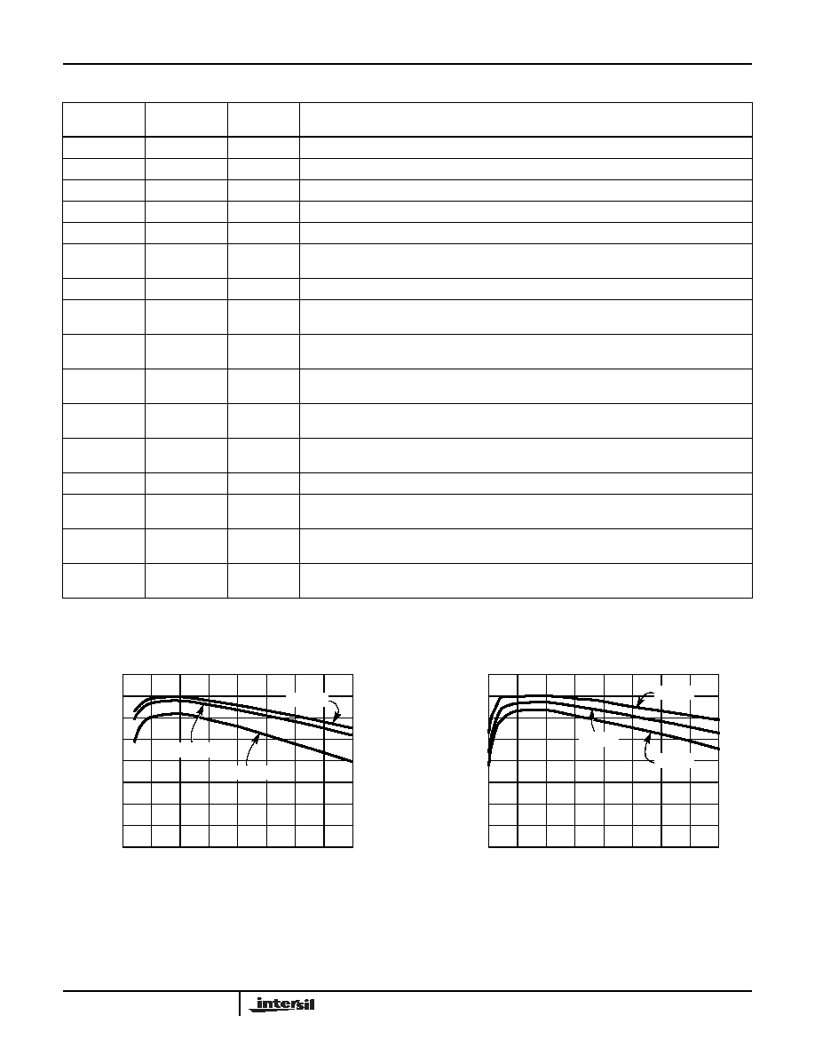
Typical Performance Curves
FIGURE 1. EL7564CM EFFICIENCY
FIGURE 2. EL7564CRE EFFICIENCY
V
IN
=5V
100
60
65
70
75
85
95
0
4
3.5
3
2.5
2
1
0.5
1.5
LOAD CURRENT I
O
(A)
EFFICIE
N
CY
(%)
V
O
=3.3V
V
O
=1.8V
80
90
V
O
=2.8V
V
IN
=5V
100
95
90
85
80
75
70
65
60
0.1
0.6
1.1
1.6
2.1
2.6
3.1
3.6
4.1
I
O
(A)
EFFICIE
N
CY
(%)
V
O
=3.3V
V
O
=1.8V
V
O
=2.5V
EL7564