1
ģ
FN7298.1
CAUTION: These devices are sensitive to electrostatic discharge; follow proper IC Handling Procedures.
1-888-INTERSIL or 321-724-7143
|
Intersil (and design) is a registered trademark of Intersil Americas Inc.
Copyright © Intersil Americas Inc. 2003-2004. All Rights Reserved.
All other trademarks mentioned are the property of their respective owners.
EL7571
Programmable PWM Controller
The EL7571 is a flexible, high efficiency, current mode, PWM
step down controller. It incorporates five bit DAC adjustable
output voltage control which conforms to the Intel Voltage
Regulation Module (VRM) Specification for Pentiumģ II and
Pentiumģ Pro class processors. The controller employs
synchronous rectification to deliver efficiencies greater than
90% over a wide range of supply voltages and load
conditions. The on-board oscillator frequency is externally
adjustable, or may be slaved to a system clock, allowing
optimization of RFI performance in critical applications. In
single supply operation, the high side FET driver supports
boot-strapped operation. For maximum flexibility, system
operation is possible from either a 5V rail, a single 12V rail,
or dual supply rails with the controller operating from 12V
and the power FETs from 5V.
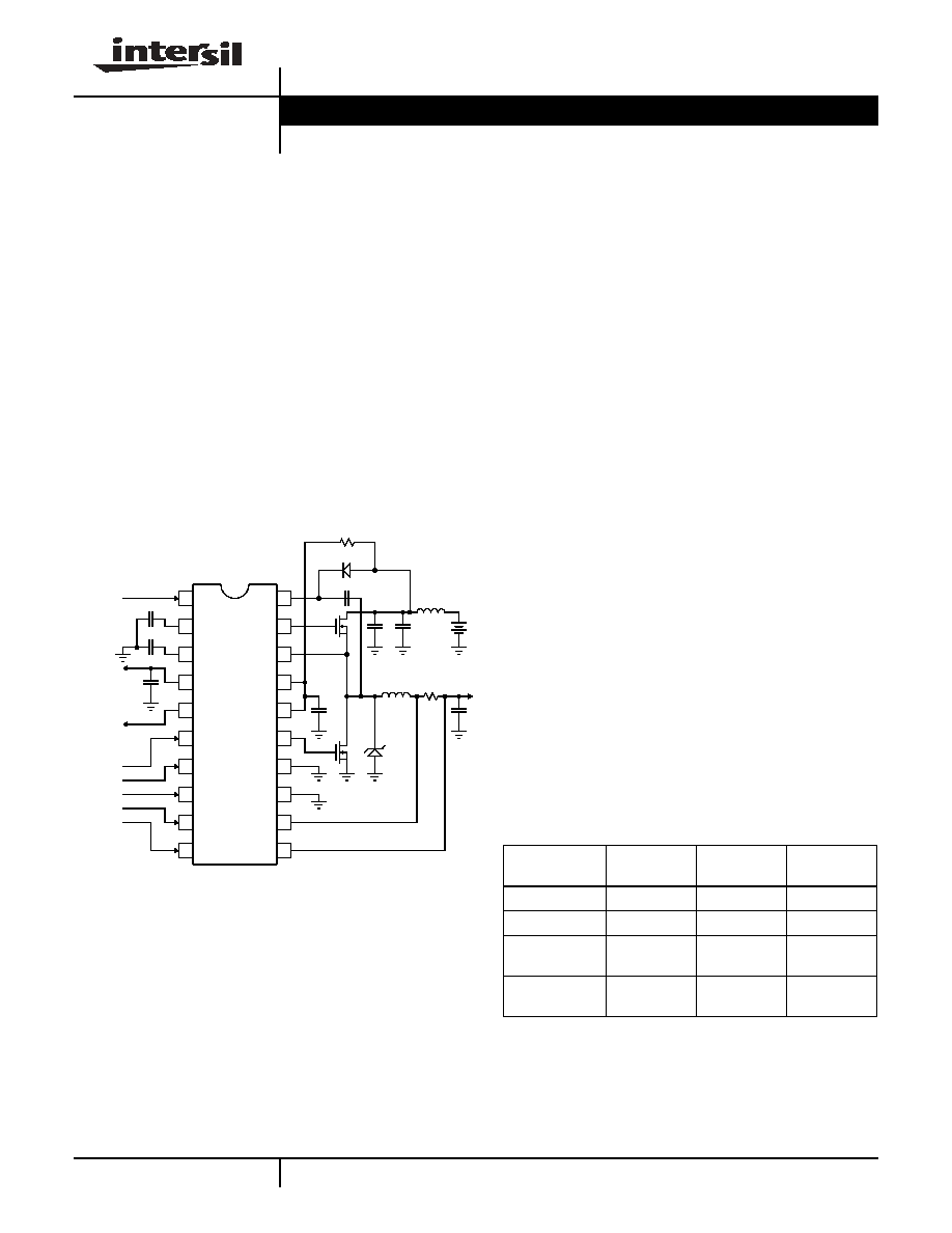
Pinout
Features
∑ Pentiumģ II Compatible
∑ 5 bit DAC Controlled Output Voltage
∑ Greater than 90% Efficiency
∑ 4.5V to 12.6V Input Range
∑ Dual NMOS Power FET Drivers
∑ Fixed frequency, Current Mode Control
∑ Adjustable Oscillator with External Sync. Capability
∑ Synchronous Switching
∑ Internal Soft-Start
∑ User Adjustable Slope Compensation
∑ Pulse by Pulse Current Limiting
∑ 1% Typical Output Accuracy
∑ Power Good Signal
∑ Output Power Down
∑ Over Voltage Protection
∑
Pb-Free Available (RoHS Compliant)
Applications
∑ Pentiumģ II Voltage Regulation Modules (VRMs)
∑ PC Motherboards
∑ DC/DC Converters
∑ GTL Bus Termination
∑ Secondary Regulation
1
2
3
4
16
15
14
13
5
6
7
12
11
9
8
10
20
19
18
17
OTEN
VID4
VID3
VID2
VID1
VIDO
PWRGD
REF
COSC
CSLOPE
VH1
FB
CS
GND
GNDP
LSD
VINP
VIN
LX
HSD
ENABLE
POWER
GOOD
Voltage
I.D. (VID
(0:4))
C3 240pF
C3 240pF
C3
0.1ĶF
1.4V
C6 0.1ĶF
R2
5
D1
Q1
C8
1ĶF
C1
1000Ķ
F x3
L2
1.5ĶH
4.5V
to
12.6V
L1
5.1ĶH
R2
5
C2
1000ĶF
x6
C7
1ĶF
Q2
D2
V
OUT
1.3V to
3.5V
Q1, Q2: Siliconix, Si4410, x2
C1: Sanyo, 16MV 1000GX, 1000ĶF x3
C2: Sanyo, 6MV 1000GX, 1000ĶF x6
L1: Pulse Engineering, PE-53700, 5.1ĶH
L2: Micrometals, T30-26, 7T AWG #20, 1.5ĶH
R1: Dale, WSL-25-12, 15m
, x2
D1: BAV99
D2: IR, 32CTQ030
Ordering Information
PART NUMBER
PACKAGE
TAPE AND
REEL
PKG. DWG. #
EL7571CM
20-Pin SO
-
MDP0027
EL7571CM-T13
20-Pin SO
13"
MDP0027
EL7571CMZ
(See Note)
20-Pin SO
(Pb-free)
-
MDP0027
EL7571CMZ-T13
(See Note)
20-Pin SO
(Pb-free)
13"
MDP0027
NOTE: Intersil Pb-free products employ special Pb-free material
sets; molding compounds/die attach materials and 100% matte tin
plate termination finish, which are RoHS compliant and compatible
with both SnPb and Pb-free soldering operations. Intersil Pb-free
products are MSL classified at Pb-free peak reflow temperatures that
meet or exceed the Pb-free requirements of IPC/JEDEC J STD-020C.
Data Sheet
October 25, 2004

2
Absolute Maximum Ratings
(T
A
= 25įC)
Supply Voltage: . . . . . . . . . . . . . . . . . . . . . . . . . . . . . . . -0.5V to 14V
Input Pin Voltage:. . . . . . . . . -.03 below Ground, +0.3 above Supply
VHI . . . . . . . . . . . . . . . . . . . . . . . . . . . . . . . . . . . . . . . . . -0.5V to 27V
Storage Temperature Range:. . . . . . . . . . . . . . . . . . 65įC to +150įC
Operating Temperature Range: . . . . . . . . . . . . . . . . . . 0įC to +70įC
Operating Junction Temperature:. . . . . . . . . . . . . . . . . . . . . . . 125įC
Peak Output Current: . . . . . . . . . . . . . . . . . . . . . . . . . . . . . . . . . . .3A
Power Dissipation: . . . . . . . . . . . . . . . . . . . . . . . . . . . .SO20 500mW
CAUTION: Stresses above those listed in "Absolute Maximum Ratings" may cause permanent damage to the device. This is a stress only rating and operation of the
device at these or any other conditions above those indicated in the operational sections of this specification is not implied.
IMPORTANT NOTE: All parameters having Min/Max specifications are guaranteed. Typical values are for information purposes only. Unless otherwise noted, all tests
are at the specified temperature and are pulsed tests, therefore: T
J
= T
C
= T
A
DC Electrical Specifications
T
A
= 25įC, V
IN
= 5V, C
OSC
= 330pF, C
SLOPE
= 390pF, R
SENSE
= 7.5m
unless otherwise specified.
PARAMETER
DESCRIPTION
CONDITION
MIN
TYP
MAX
UNIT
V
IN
Input Voltage Range
4.5
12.6
V
V
UVLO HI
Input Under Voltage Lock out Upper
Limit
Positive going input voltage
3.6
4
4.4
V
V
UVLO LO
Input Under Voltage Lock out Lower
Limit
Negative going input voltage
3.15
3.5
3.85
V
V
OUT RANGE
Output Voltage Range
See VID table
1.3
3.5
V
V
OUT 1
Steady State Output Voltage Accuracy,
VID = 10111
I
L
= 6.5A, V
OUT
= 2.8V
2.74
2.82
2.90
V
V
OUT 2
Steady State Output Voltage Accuracy,
VID = 00101
I
L
= 6.5A, V
OUT
=1.8V
1.74
1.81
1.9
V
V
REF
Reference Voltage
1.396
1.41
1.424
V
V
ILIM
Current Limit Voltage
V
ILIM
= (V
CS
-V
FB
)
125
154
185
mV
V
IREV
Current Reversal Threshold
V
IREV
= (V
CS
-V
FB
)
-40
-5
20
mV
V
OUT PG
Output Voltage Power Good Lower
Level
V
OUT
= 2.05V
-18
-14
-10
%
Output Voltage Power Good Upper
Level
8
12
16
%
V
OVP
Over-Voltage Protection Threshold
+9
+13
+17
%
V
OTEN LO
Power Down Input Low Level
V
IN
= -10uA
1.5
V
V
OTEN HI
Power Down Input High Level
(V
IN
-1.5)
V
V
ID LO
Voltage I.D. Input Low Level
1.5
V
V
ID HI
Voltage I.D. Input High Level
(V
IN
-1.5)
V
V
OSC
Oscillator Voltage Swing
0.85
V
P-P
V
PWRGD LO
Power Good Output Low Level
I
OUT
= 1mA
0.5
V
R
DS ON
HSD, LSD Switch On-Resistance
V
IN
, V
INP
= 12V, I
OUT
= 100mA,
(VHI-LX) = 12V
4.8
6
R
FB
FB Input Impedance
9.5
k
R
CS
CS Input Impedance
115
k
I
VIN
Quiescent Supply Current
V
OTEN
>(V
IN
-0.5)V
1.2
2
mA
I
VIN DIS
Supply Current in Output Disable Mode
V
OTEN
<1.5V
0.76
1
mA
I
SOURCE/SINK
Peak Driver Output Current
V
IN
,V
INP
= 12V, Measured at HSD,
LSD, (VHI-LX) = 12V
2.5
A
I
RAMP
C
SLOPE
Ramp Current
High Side Switch Active
8.5
14
20
ĶA
I
OSC CHARGE
Oscillator Charge Current
1.2>V
OSC
>0.35V
50
ĶA
I
OSC DISCHARGE
Oscillator Discharge Current
1.2>V
OSC
>0.35V
2
mA
I
REFMAX
VREF Output Current
25
ĶA
EL7571
3
NOTE: Pin designators: I = Input, O = Output, S = Supply
I
VID
VID Input Pull up Current
3
5
7
ĶA
I
OTEN
OTEN Input Pull up Current
3
5
7
ĶA
DC Electrical Specifications
T
A
= 25įC, V
IN
= 5V, C
OSC
= 330pF, C
SLOPE
= 390pF, R
SENSE
= 7.5m
unless otherwise specified.
(Continued)
PARAMETER
DESCRIPTION
CONDITION
MIN
TYP
MAX
UNIT
AC Electrical Specifications
T
A
= 25įC, V
IN
= 5V, C
OSC
= 330pF, C
SLOPE
= 390pF unless otherwise specified.
PARAMETER
DESCRIPTION
CONDITIONS
MIN
TYP
MAX
UNIT
f
OSC
Nominal Oscillator Frequency
C
OSC
= 330pF
140
190
240
kHz
f
CLK
Clock Frequency
50
500
1000
kHz
t
OTEN
Shutdown Delay
V
OTEN
>1.5V
100
ns
t
SYNC
Oscillator Sync. Pulse Width
Oscillator i/p (COSC) driven with
HCMOS gate
20
800
ns
T
START
Soft-start Period
V
OUT
= 3.5V
100/f
CLK
us
D
MAX
Maximum Duty Cycle
97
%
Pin Descriptions
PIN NO.
PIN NAME
PIN TYPE
(NOTE 1)
FUNCTION
1
OTEN
I
Chip enable input, internal pull up (5mA typical). Active high.
2
CSLOPE
I
With a capacitor attached from CSLOPE to GND, generates the voltage ramp compensation for the PWM
current mode controller. Slope rate is determined by an internal 14uA pull up and the C
SLOPE
capacitor
value. VC
SLOPE
is reset to ground at the termination of the high side cycle.
3
COSC
I
Multi-function pin: with a timing capacitor attached, sets the internal oscillator rate f
S
(kHz) = 57/C
OSC
(ĶF);
when pulsed low for a duration t
SYNC
synchronizes device to an external clock.
4
REF
O
Band gap reference output. Decouple to GND with 0.1uF.
5
PWRGD
O
Power good, open drain output. Set low whenever the output voltage is not within Ī13% of the programmed
value.
6
VID0
I
Bit 0 of the output voltage select DAC. Internal pull up sets input high when not driven.
7
VID1
I
Bit 1 of the output voltage select DAC. Internal pull up sets input high when not driven.
8
VID2
I
Bit 2 of the output voltage select DAC. Internal pull up sets input high when not driven.
9
VID3
I
Bit 3 of the output voltage select DAC. Internal pull up sets input high when not driven.
10
VID4
I
Bit 4 of the output voltage select DAC. Internal pull up sets input high when not driven.
11
FB
I
Voltage regulation feedback input. Tie to V
OUT
for normal operation.
12
CS
I
Current sense. Current feedback input of PWM controller and over current capacitor input. Current limit
threshold set at +154mV with respect to FB. Connect sense resistor between CS and FB for normal
operation.
13
GND
S
Ground
14
GNDP
S
Power ground for low side FET driver. Tie to GND for normal operation.
15
LSD
O
Low side gate drive output.
16
VINP
S
Input supply voltage for low side FET driver. Tie to VIN for normal operation.
17
VIN
S
Input supply voltage for control unit.
18
LX
S
Negative supply input for high side FET driver.
19
HSD
O
High side gate drive output. Driver ground referenced to LX. Driver supply may be bootstrapped to enhance
low controller input voltage operation.
20
VH1
S
Positive supply input for high side FET driver.
EL7571
4
Typical Performance Curves
+12V Supply Sync Line Regulation
-0.002
0.004
0.003
0.002
0.001
0
-0.001
-0.003
Line R
e
gulation
(%)
V
IN
(V)
13.5
10.0
11.5
11.0
10.5
13.0
12.5
12.0
5V Supply Line Regulation
-0.30
0.30
0.20
0.10
0.00
-0.10
-0.20
-0.40
Line Regulation (%)
V
IN
(V)
5.50
4.50
5.00
5.25
4.75
+12V Supply Sync Efficiency
1.0
E
f
f
i
c
i
ency (
%
)
I
OUT
(A)
0.8
0.7
0.6
0.5
0.9
+12V Supply Sync Load Regulation
0.04
Load Regulation (%)
I
OUT
(A)
0.02
0
-0.01
-0.02
0.03
0.01
VRM +5V Supply +12V Controller Sync w/o Schottky Load
Regulation
6.00
L
o
ad Regulat
i
on (
%
)
I
OUT
(A)
3.00
1.00
-1.00
-2.00
5.00
2.00
+5V Supply Non-Sync Load Regulation
5.00
Lo
ad Regulation (%)
I
OUT
(A)
2.00
0
-1.00
-2.00
4.00
1.00
3.00
4.00
0
V
OUT
= 2.1V
V
OUT
= 2.8V
0
1
3
5
11
13
9
7
0
1
3
5
11
13
9
7
0
1
3
5
11
13
9
7
0
1
3
5
11
13
9
7
V
OUT
= 1.8V
V
OUT
= 1.3V
V
OUT
= 2.8V
V
OUT
= 3.5V
V
OUT
= 1.8V
V
OUT
= 1.8V
V
OUT
= 2.8V
V
OUT
= 3.5V
V
OUT
= 1.3V
V
OUT
= 3.5V
V
OUT
= 1.8V
V
OUT
= 2.8V
EL7571
5
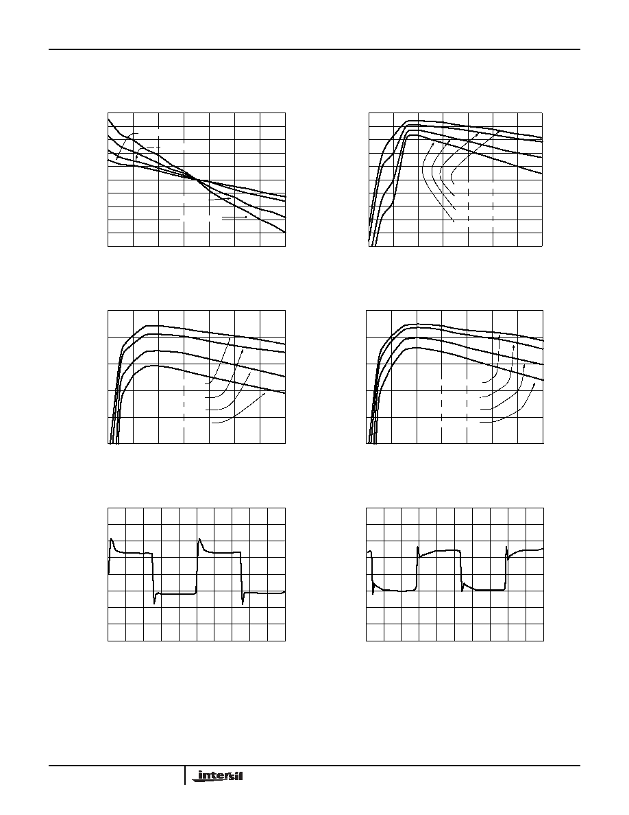
Typical Performance Curves
(Continued)
5V Non-sync Transient Response
1
12V Transient Response
1
+5V Supply +12V Controller Sync w/o Schottky VRM
Efficiency
1.0
Ef
ficie
n
c
y
(X
)
I
OUT
(A)
0.02
0.8
0.7
0.6
0.5
0.9
1.02
3.04
5.04
11.04
13.04
9.04
7.04
+5V Supply Sync with Schottky Load
2.5
Load Regulation
(
%
)
I
OUT
(A)
0
0.5
-0.5
-1.5
-2.5
1.5
1
3
5
11
13
9
7
0
+5V Supply Non-Sync VRM Efficiency
Ef
fi
ci
en
c
y
(
%
)
I
OUT
(A)
1.0
0.8
0.7
0.6
0.5
0.9
+5V Supply Sync with Schottky VRM Efficiency
Ef
fi
ci
en
c
y
(
%
)
I
OUT
(A)
1.0
0.8
0.7
0.6
0.5
0.9
0
1
3
5
11
13
9
7
0
1
3
5
11
13
9
7
V
OUT
= 1.8V
V
OUT
= 1.3V
V
OUT
= 2.8V
V
OUT
= 3.5V
V
OUT
= 1.8V
V
OUT
= 2.8V
V
OUT
= 1.3V
V
OUT
= 3.5V
V
OUT
= 3.5V
V
OUT
= 1.3V
V
OUT
= 1.8V
V
OUT
= 2.8V
V
OUT
= 3.5V
V
OUT
= 1.3V
V
OUT
= 1.8V
V
OUT
= 2.8V
EL7571