Äîêóìåíòàöèÿ è îïèñàíèÿ www.docs.chipfind.ru
1
®
FN7317.2
EL7584
4-Channel DC/DC Converter
The EL7584 is a 4-channel DC/DC converter IC which is
designed primarily for use in TFT-LCD applications. The
boost converter has 2V to 14V input capability and provides
5V to 17V output, which powers the column drivers and
provides up to 370mA @ 15V. A pair of charge pump control
circuits provide outputs to allow the external generation of
V
ON
and V
OFF
supplies at 5V to 40V and 0V to -40V,
respectively, each at up to 60mA for V
BOOST
= 15V. The
V
COM
buffer provides up to 50mA continuous output current
from 2V to 13V.
The EL7584 features adjustable switching frequency and on-
chip power sequence to simplify start-up operation. A
separate input is available to externally increase the default
delay of the positive charge pump. An over-temperature
feature is provided to allow the IC to be automatically
protected from excessive power dissipation.
The EL7584 is available in a 24-pin TSSOP package and is
specified for operation over the full -40°C to +85°C
temperature range.
Pinout
EL7584
(24-PIN TSSOP)
TOP VIEW
SS
FBB
EN
VDDB
LX1
LX2
VSSN
DRVN
VDDN
FBN
DP
INC
VSSB
ROSC
VREF
PGND
PGND
VSSP
DRVP
VDDP
FBP
VSSC
VCOM
VDDC
1
2
3
4
16
15
14
13
5
6
7
12
11
9
8
10
20
19
18
17
24
23
22
21
Features
· TFT-LCD display supply
- Boost regulator
- V
COM
buffer
- V
ON
charge pump
- V
OFF
charge pump
· 2V to 14V V
IN
supply
· 5V < V
BOOST
< 17V
· 2V < V
COM
< 13V
· 5V < V
ON
< 40V
· -40V < V
OFF
< 0V
· V
BOOST
= 15V @ 370mA
· High frequency, small inductor DC/DC boost circuit
· Over 90% efficient DC/DC boost converter capability
· Built-in power-up sequence with adjustable V
ON
delay
· Adjustable frequency
· Adjustable soft-start
· Adjustable outputs
· Over-temperature protection
· Small parts count
· Pb-free available (RoHS compliant)
Applications
· TFT-LCD panels
· PDAs
Ordering Information
PART
NUMBER
PACKAGE
TAPE & REEL
PKG. DWG. #
EL7584IR
24-Pin TSSOP
-
MDP0044
EL7584IR-T7
24-Pin TSSOP
7"
MDP0044
EL7584IR-T13
24-Pin TSSOP
13"
MDP0044
EL7584IRZ
(See Note)
24-Pin TSSOP
(Pb-free)
-
MDP0044
EL7584IRZ-T7
(See Note)
24-Pin TSSOP
(Pb-free)
7"
MDP0044
EL7584IRZ-
T13 (See Note)
24-Pin TSSOP
(Pb-free)
13"
MDP0044
NOTE: Intersil Pb-free products employ special Pb-free material sets; molding
compounds/die attach materials and 100% matte tin plate termination finish, which are
RoHS compliant and compatible with both SnPb and Pb-free soldering operations.
Intersil Pb-free products are MSL classified at Pb-free peak reflow temperatures that
meet or exceed the Pb-free requirements of IPC/JEDEC J STD-020.
Data Sheet
February 4, 2005
CAUTION: These devices are sensitive to electrostatic discharge; follow proper IC Handling Procedures.
1-888-INTERSIL or 321-724-7143
|
Intersil (and design) is a registered trademark of Intersil Americas Inc.
Copyright © Intersil Americas Inc. 2003. All Rights Reserved. Elantec is a registered trademark of Elantec Semiconductor, Inc.
All other trademarks mentioned are the property of their respective owners.
Absolute Maximum Ratings
(T
A
= 25°C)
LX Pin Voltage . . . . . . . . . . . . . . . . . . . . . . . . . . . . . . . . . . . . . . .18V
V
DDB
, V
DDP
, V
DDN
18V
V
DDC
16.5V
Maximum Continuous V
BOOST
Output Current. . . . . . . . . . . 800mA
Storage Temperature . . . . . . . . . . . . . . . . . . . . . . . .-65°C to +150°C
Ambient Operating Temperature . . . . . . . . . . . . . . . .-40°C to +85°C
Power Dissipation . . . . . . . . . . . . . . . . . . . . . . . . . . . . . See Curves
CAUTION: Stresses above those listed in "Absolute Maximum Ratings" may cause permanent damage to the device. This is a stress only rating and operation of the
device at these or any other conditions above those indicated in the operational sections of this specification is not implied.
2
FN7317.2
February 4, 2005
IMPORTANT NOTE: All parameters having Min/Max specifications are guaranteed. Typ values are for information purposes only. Unless otherwise noted, all tests are
at the specified temperature and are pulsed tests, therefore: T
J
= T
C
= T
A
. . . . . . . . . . . . . . . . . . . . . . . . . . . . . . . . . . .
. . . . . . . . . . . . . . . . . . . . . . . . . . . . . . . . . . . . . . . . . . . .
Electrical Specifications
V
IN
= 3.3V, V
BOOST
= 12V, R
OSC
= 62k
, T
A
= 25°C, Unless Otherwise Specified.
PARAMETER
DESCRIPTION
CONDITIONS
MIN
TYP
MAX
UNIT
DC/DC BOOST CONVERTER
IQ1_B
Quiescent Current - Shut-down
EN = 0V
0.8
10
µA
IQ2_B
Quiescent Current - Switching
EN = V
DDB
4.8
8
mA
V(FBB)
Feedback Voltage
1.275
1.300
1.325
V
V
REF
Reference Voltage
1.260
1.310
1.360
V
V
ROSC
Oscillator Set Voltage
1.260
1.325
1.390
V
I(FBB)
Feedback Input Bias Current
0.1
µA
V
DDB
Boost Converter Supply Range
2
17
V
D
MAX
Maximum Duty Cycle
85
92
%
I(LX)
MAX
Peak Internal FET Current
1.75
A
R
DS-ON
Switch On Resistance
at V
BOOST
= 10V, I(LX) total = 350mA
0.22
I
LEAK-SWITCH
Switch Leakage Current
I(LX) total
1
µA
V
BOOST
Output Range
V
BOOST
> V
IN
+ V
DIODE
5
17
V
V
BOOST
/
V
IN
Line Regulation
2.7V < V
IN
< 13.2V, V
BOOST
= 15V
0.1
%
V
BOOST
/
I
O1
Load Regulation
50mA < I
O1
< 250mA
0.5
%
F
OSC-RANGE
Frequency Range
R
OSC
range = 240k
to 60k
200
1200
kHz
F
OSC1
Switching Frequency
R
OSC
= 62k
900
1000
1100
kHz
V
COM
BUFFER
V
DDC
Supply Voltage Range
6
15
V
IQ1, V
DDC
V
DDC
Disable Current
V
DDC
= 12V, EN = 0V
5.5
20
µA
IQ2, V
DDC
V
DDC
Enable Current
V
DDC
= 12V, V
EN
= V
DDB
, no load
1.7
5
mA
V
COM
-offset
Accuracy of V
COM
Output Voltage
2V < V
COM
< (V
DDC
- 2V)
-10
+10
mV
I(INC)
V
COM
Input Bias Currents
Current magnitude
-0.1
0.01
0.1
µA
R
O
(V
COM
)
V
COM
Output Impedance
V
DDC
= V
BOOST
= 12V, V
COM
= 6V with
-100mA < I
LOAD
< 100mA
C
LOAD
for V
COM
> 0.47µF, MLCC
0.25
I
COM
(max)
Output Current Limit
150
mA
PSRR
Supply Voltage Rejection
V
INC
= V
DDC/2
, 9V < V
DDC
< 15V
60
102
dB
CMRR
Common Mode Voltage Rejection
V
DDC
= 12V, 2V < V
INC
< 10V
60
93
dB
EL7584
3
FN7317.2
February 4, 2005
POSITIVE REGULATED CHARGE PUMP (V
ON
)
Most positive V
ON
output depends on the magnitude of the V
DDP
input voltage (normally connected to V
BOOST
) and the external component
configuration (doubler or tripler)
V
DDP
Supply Input for Positive Charge Pump
Usually connected to V
BOOST
output
5
17
V
IQ1(V
DDP
)
Quiescent Current - Shut-down
EN = 0V
11.5
20
µA
IQ2(V
DDP
)
Quiescent Current - Switching
EN = V
DDB
2.3
5
mA
I
DP1
Disable Charge Current
EN = 0V, DP = 0V
1.5
1.9
2.5
mA
I
DP2
Enable Discharge Current
EN = V
DDB
, DP = 5V
100
200
300
nA
V(FBP)
Feedback Reference Voltage
1.245
1.310
1.375
V
I(FBP)
Feedback Input Bias Current
0.1
µA
I(DRVP)
RMS DRVP Output Current
V
DDP
= 12V
60
mA
V
DDP
= 6V
15
mA
ILR_V
ON
Load Regulation
5mA < I
L
< 15mA
-0.5
0.03
0.5
%/mA
F
PUMP
Charge Pump Frequency
Frequency set by R
OSC
- see boost section
0.5*F
OSC
NEGATIVE REGULATED CHARGE PUMP (V
OFF
)
Most negative V
OFF
output depends on the magnitude of the V
DDN
input voltage (normally connected to V
BOOST
) and the external component
configuration (doubler or tripler)
V
DDN
Supply Input for Negative Charge Pump
Usually connected to V
BOOST
output
5
17
V
IQ1(V
DDN
)
Quiescent Current - Shut-down
ENBN = 0V
4.5
20
µA
IQ2(V
DDN
)
Quiescent Current - Switching
ENBN = V
DDB
2.3
5
mA
V(FBN)
Feedback Reference Voltage
-80
0
+80
mV
I(FBN)
Feedback Input Bias Current
Magnitude of input bias
0.1
µA
I(DRVN)
RMS DRVN Output Current
V
DDN
= 12V
60
mA
V
DDN
= 6V
15
mA
ILR_V
OFF
Load Regulation
-15mA < I
L
< -5mA
-0.5
0.03
0.5
%/mA
F
PUMP
Charge Pump Frequency
Frequency set by R
OSC
- see boost section
0.5*F
OSC
ENABLE CONTROL LOGIC
V
HI
-EN
Enable Input High Threshold
1.6
V
V
LO
-EN
Enable Input Low Threshold
0.5
V
I(EN)
Enable Input Bias Current
V
EN
= 5V
3.7
7.5
µA
OVER-TEMPERATURE PROTECTION
T
OT
Over-temperature Threshold
130
°C
T
HYS
Over-temperature Hysteresis
40
°C
Electrical Specifications
V
IN
= 3.3V, V
BOOST
= 12V, R
OSC
= 62k
, T
A
= 25°C, Unless Otherwise Specified. (Continued)
PARAMETER
DESCRIPTION
CONDITIONS
MIN
TYP
MAX
UNIT
EL7584
Pin Descriptions
I = Input, O = Output, S = Supply
PIN NUMBER
PIN NAME
PIN TYPE
PIN FUNCTION
1
SS
I
Soft-Start input: a capacitor determines the current limit ramp time.
2
FBB
I
Voltage feedback input determines the value of V
BOOST
.
3
EN
I
Starts internal power sequencing of V
BOOST
, V
OFF
, V
COM
and V
ON
outputs
(See Applications Information) ; active HIGH input.
4
VDDB
P
Positive supply for V
BOOST
DC/DC controller.
5
LX1
O
Boost inductor saturating MOSFET #1.
6
LX2
O
Boost inductor saturating MOSFET #2.
7
VSSN*
P
Ground return for V
OFF
regulator.
8
DRVN
O
Pump capacitor driver for V
OFF
regulator.
9
VDDN
P
Positive supply for V
OFF
regulator.
10
FBN
I
Voltage feedback input determines the value of V
OFF
.
11
DP
I
An external capacitor increases V
ON
power up delay time.
12
INC
I
V
COM
Buffer input.
13
VDDC
P
Positive supply for V
COM
Buffer.
14
VCOM
O
V
COM
Buffer output.
15
VSSC*
P
Ground return for V
COM
Buffer.
16
FBP
I
Voltage feedback input determines the value of V
ON
.
17
VDDP
P
Positive supply for V
ON
regulator.
18
DRVP
O
Pump capacitor driver for V
ON
regulator.
19
VSSP*
P
Ground return for V
ON
regulator.
20
PGND*
P
Ground return for MOSFET #1.
21
PGND*
P
Ground return for MOSFET #2.
22
VREF
O
Voltage reference for V
OFF
feedback .
23
ROSC
I
An external resistor sets the DC/DC switching frequency.
24
VSSB*
P
Ground return for V
BOOST
DC/DC controller.
NOTE: *VSSB, VSSC, VSSN, VSSP, and PGND (2) are shorted internally to the device substrate.
4
FN7317.2
February 4, 2005
EL7584
5
FN7317.2
February 4, 2005
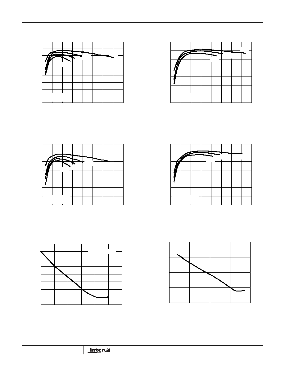
Typical Performance Curves
FIGURE 1. EFFICIENCY vs I
OUT
0
100
200
300
400
500
600
700
800
95
90
85
80
75
70
65
60
55
50
I
OUT
(mA)
E
F
F
I
CIENCY (%
)
V
IN
=3.3V
FREQ=1MHz
15V
12V
9V
5V
FIGURE 2. EFFICIENCY vs I
OUT
0
100
200
300
400
500
600
700
800
95
90
85
80
75
70
65
60
I
OUT
(mA)
E
F
F
I
CIENCY (%
)
V
IN
=5V
FREQ=1MHz
15V
12V
9V
FIGURE 3.
0
100
200
300
400
500
600
700
800
95
90
85
80
75
70
65
60
I
OUT
(mA)
EFF
I
CIENCY (%
)
V
IN
=3.3V
FREQ=700kHz
15V
12V
9V
5V
EFFICIENCY vs I
OUT
FIGURE 4.
0
100
200
300
400
500
600
700
800
95
90
85
80
75
65
60
I
OUT
(mA)
EFF
I
CIENCY (%
)
V
IN
=5V
FREQ=700kHz
15V
12V
9V
70
EFFICIENCY vs I
OUT
FIGURE 5.
970
968
966
964
962
3
3.5
6
V
DDB
(V)
FR
E
Q
UENCY (k
H
z
)
4.5
965
963
5.5
969
4
5
967
R
OSC
= 61.9k
F
S
vs V
DDB
FIGURE 6.
1.27
1.26
1.25
-50
150
TEMPERATURE (°C)
VOL
T
AG
E (V)
50
1.265
0
100
1.255
V
REF
vs TEMPERATURE
EL7584