EL7585A
1
®
FN7523.2
EL7585A
TFT-LCD Power Supply
The EL7585A represents a multiple output regulators for use
in all large panel, TFT-LCD applications. It features a single
boost converter with integrated 3.5A FET, two positive LDOs
for V
ON
and V
LOGIC
generation, and a single negative LDO
for V
OFF
generation. The boost converter can be
programmed to operate in either P-mode or PI-mode for
improved load regulation.
The EL7585A also integrates fault protection for all four
channels. Once a fault is detected, the device is latched off
until the input supply or EN is cycled. This device also
features an integrated start-up sequence for V
BOOST,
V
OFF
,
then V
ON
or for V
OFF
, V
BOOST
, and V
ON
sequencing. The
latter requires a single external transistor. The timing of the
start-up sequence is set using an external capacitor. The
V
LOGIC
output is constantly enabled, but does shut down
when a fault condition is detected.
The EL7585A is specified for operation over the -40°C to
+85°C temperature range.
Features
· 3.5A current limit FET options
· 3V to 5V input
· Up to 20V boost out
· 1% regulation on all outputs
· V
OFF
-V
BOOST
-V
ON
or
V
BOOST
-V
OFF
-V
ON
sequence control
- V
LOGIC
is on from start-up for EL7585A
· Programmable sequence delay
· Fully fault protected
· Thermal shutdown
· Internal soft-start
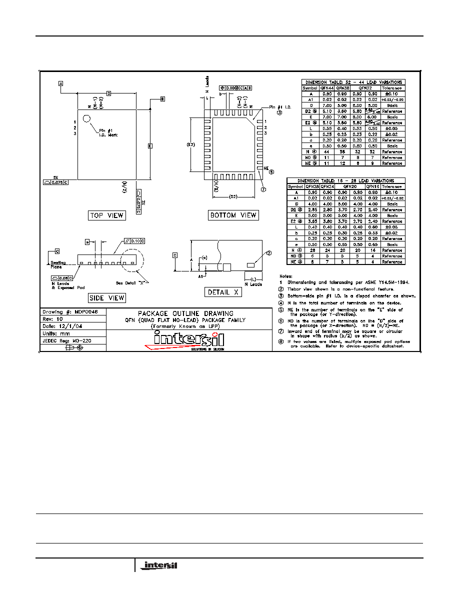
· 20 Ld QFN packages
· Pb-free plus anneal available (RoHS compliant)
Applications
· LCD monitors (15"+)
· LCD-TV (up to 40"+)
· Notebook displays (up to 16")
· Industrial/medical LCD displays
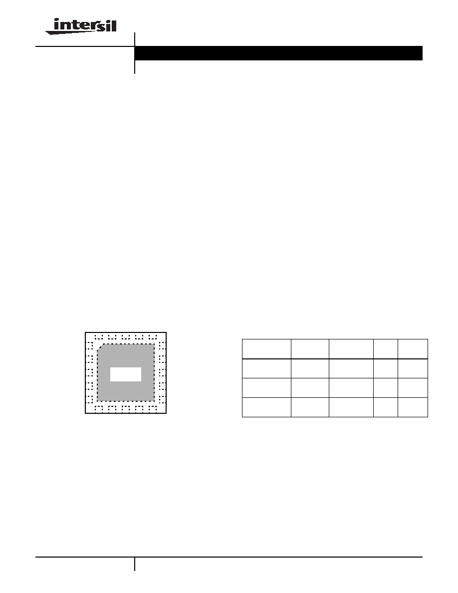
Pinout
EL7585A
(20 LD QFN)
TOP VIEW
1
2
3
4
15
14
13
12
6
7
8
9
20
19
18
17
CDLY
DELB
LX1
LX2
FBP
DR
V
L
FBL
SG
ND
PG
VD
D
EN
SG
N
D
CINT
VREF
PGND
PGND
THERMAL
PAD
5
DRVP
10
DR
V
N
11 FBN
16
FBB
Ordering Information
PART NUMBER
PART
MARKING
PACKAGE
TAPE &
REEL
PKG.
DWG. #
EL7585AILZ
(Note)
EL7585AIL Z 20 Ld 4x4 QFN
(Pb-free)
-
MDP0046
EL7585AILZ-T7
(Note)
EL7585AIL Z 20 Ld 4x4 QFN
(Pb-free)
7"
MDP0046
EL7585AILZ-T13
(Note)
EL7585AIL Z 20 Ld 4x4 QFN
(Pb-free)
13"
MDP0046
NOTE: Intersil Pb-free plus anneal products employ special Pb-free
material sets; molding compounds/die attach materials and 100%
matte tin plate termination finish, which are RoHS compliant and
compatible with both SnPb and Pb-free soldering operations. Intersil
Pb-free products are MSL classified at Pb-free peak reflow
temperatures that meet or exceed the Pb-free requirements of
IPC/JEDEC J STD-020.
Data Sheet
September 21, 2005
CAUTION: These devices are sensitive to electrostatic discharge; follow proper IC Handling Procedures.
1-888-INTERSIL or 1-888-468-3774
|
Intersil (and design) is a registered trademark of Intersil Americas Inc.
Copyright Intersil Americas Inc. 2005. All Rights Reserved
All other trademarks mentioned are the property of their respective owners.
2
FN7523.2
September 21, 2005
Absolute Maximum Ratings
(T
A
= 25°C)
V
DRVP
. . . . . . . . . . . . . . . . . . . . . . . . . . . . . . . . . . . . . . . . . . . . .36V
V
DRVN
. . . . . . . . . . . . . . . . . . . . . . . . . . . . . . . . . . . . . . . . . . . . -20V
V
DD
. . . . . . . . . . . . . . . . . . . . . . . . . . . . . . . . . . . . . . . . . . . . . . 6.5V
V
DELB,
V
LX
. . . . . . . . . . . . . . . . . . . . . . . . . . . . . . . . . . . . . . . . .24V
V
DRVL
. . . . . . . . . . . . . . . . . . . . . . . . . . . . . . . . . . . . . . . . . . . . 6.5V
Storage Temperature . . . . . . . . . . . . . . . . . . . . . . . .-65°C to +150°C
Ambient Operating Temperature . . . . . . . . . . . . . . . .-40°C to +85°C
Power Dissipation . . . . . . . . . . . . . . . . . . . . . . . . . . . . . See Curves
Maximum continuous junction temperature . . . . . . . . . . . . . . 125°C
CAUTION: Stresses above those listed in "Absolute Maximum Ratings" may cause permanent damage to the device. This is a stress only rating and operation of the
device at these or any other conditions above those indicated in the operational sections of this specification is not implied.
IMPORTANT NOTE: All parameters having Min/Max specifications are guaranteed. Typical values are for information purposes only. Unless otherwise noted, all tests
are at the specified temperature and are pulsed tests, therefore: T
J
= T
C
= T
A
Electrical Specifications
V
DD
= 5V, V
BOOST
= 11V, I
LOAD
= 200mA, V
ON
= 15V, V
OFF
= -5V, V
LOGIC
= 2.5V, over temperature from
-40°C to 85°C, unless otherwise specified.
PARAMETER
DESCRIPTION
CONDITION
MIN
TYP
MAX
UNIT
SUPPLY
V
S
Supply Voltage
3
5.5
V
I
S
Quiescent Current
Enabled, LX not switching
1.7
2.5
mA
Disabled
700
900
µA
CLOCK
F
OSC
Oscillator Frequency
900
1000
1100
kHz
BOOST
V
BOOST
Boost Output Range
5.5
20
V
V
FBB
Boost Feedback Voltage
T
A
= 25°C
1.192
1.205
1.218
V
1.188
1.205
1.222
V
V
F_FBB
FBB Fault Trip Point
0.9
V
V
REF
Reference Voltage
T
A
= 25°C
1.19
1.215
1.235
V
1.187
1.215
1.238
V
C
REF
V
REF
Capacitor
22
100
nF
D
MAX
Maximum Duty Cycle
85
%
I
LXMAX
Switch Current Limit
3.5
A
I
LEAK
Switch Leakage Current
V
LX
= 16V
10
µA
r
DS(ON)
Switch On-Resistance
160
m
Eff
Boost Efficiency
See curves
92
%
I(V
FBB
)
Feedback Input Bias Current
Pl mode, V
FBB
= 1.35V
50
500
nA
V
BOOST
/
V
IN
Line Regulation
C
INT
= 4.7nF, I
OUT
= 100mA, V
IN
= 3V to 5.5V
0.05
%/V
V
BOOST
/
I
BOOST
Load Regulation - "P" mode
C
INT
pin strapped to V
DD
,
50mA < I
LOAD
< 250mA
3
%
V
BOOST
/
I
BOOST
Load Regulation - "PI" mode
C
INT
= 4.7nF, 50mA < I
O
< 250mA
0.1
%
V
CINT_T
CINT Pl Mode Select Threshold
4.7
4.8
V
V
ON
LDO
V
FBP
FBP Regulation Voltage
I
DRVP
= 0.2mA, T
A
= 25°C
1.176
1.2
1.224
V
I
DRVP
= 0.2mA
1.172
1.2
1.228
V
V
F_FBP
FBP Fault Trip Point
V
FBP
falling
0.82
0.87
0.92
V
I
FBP
FBP Input Bias Current
V
FBP
= 1.35V
-250
250
nA
GMP
FBP Effective Transconductance
V
DRVP
= 25V, I
DRVP
= 0.2 to 2mA
50
ms
EL7585A
3
FN7523.2
September 21, 2005
V
ON
/
I(V
ON
) V
ON
Load Regulation
I(V
ON
) = 0mA to 20mA
-0.5
%
I
DRVP
DRVP Sink Current Max
V
FBP
= 1.1V, V
DRVP
= 25V
2
4
mA
I
L_DRVP
DRVP Leakage Current
V
FBP
= 1.5V, V
DRVP
= 35V
0.1
5
µA
V
OFF
LDO
V
FBN
FBN Regulation Voltage
I
DRVN
= 0.2mA, T
A
= 25°C
0.173
0.203
0.233
V
I
DRVN
= 0.2mA
0.171
0.203
0.235
V
V
F_FBN
FNN Fault Trip Point
V
FBN
rising
0.38
0.43
0.48
V
I
FBN
FBN Input Bias Current
V
FBN
= 0.2V
-250
250
nA
GMN
FBN Effective Transconductance
V
DRVN
= -6V, I
DRVN
= 0.2mA to 2mA
50
ms
V
OFF
/
I(V
OFF
)
V
OFF
Load Regulation
I(V
OFF
) = 0mA to 20mA
-0.5
%
I
DRVN
DRVN Source Current Max
V
FBN
= 0.3V, V
DRVN
= -6V
2
4
mA
I
L_DRVN
DRVN Leakage Current
V
FBN
= 0V, V
DRVN
= -20V
0.1
5
µA
V
LOGIC
LDO
V
FBL
FBL Regulation Voltage
I
DRVL
= 1mA, T
A
= 25°C
1.176
1.2
1.224
V
I
DRVL
= 1mA
1.174
1.2
1.226
V
V
F_FBL
FBL Fault Trip Point
V
FBL
falling
0.82
0.87
0.92
V
I
FBL
FBL Input Bias Current
V
FBL
= 1.35V
-500
500
nA
G
ML
FBL Effective Transconductance
V
DRVL
= 2.5V, I
DRVL
= 1mA to 8mA
200
ms
V
LOGIC
/
I(V
LOGIC
)
V
LOGIC
Load Regulation
I(V
LOGIC
) = 100mA to 500mA
0.5
%
I
DRVL
DRVL Sink Current Max
V
FBL
= 1.1V, V
DRVL
= 2.5V
8
16
mA
I
L_DRL
I
L_DRVL
V
FBL
= 1.5V, V
DRVL
= 5.5V
0.1
5
µA
SEQUENCING
t
ON
Turn On Delay
C
DLY
= 0.22µF
30
ms
t
SS
Soft-start Time
C
DLY
= 0.22µF
2
ms
t
DEL1
Delay Between A
VDD
and V
OFF
C
DLY
= 0.22µF
10
ms
t
DEL2
Delay Between V
ON
and V
OFF
C
DLY
= 0.22µF
17
ms
t
DEL3
Delay Between V
OFF
and Delayed
V
BOOST
C
DLY
= 0.22µF
10
ms
I
DELB
DELB Pull-down Current
V
DELB
> 0.6V
50
µA
V
DELB
< 0.6V
1.4
mA
C
DEL
Delay Capacitor
10
220
nF
FAULT DETECTION
t
FAULT
Fault Time Out
C
DLY
= 0.22µF
50
ms
OT
Over-temperature Threshold
140
°C
I
PG
PG Pull-down Current
VPG>0.6V
15
µA
VPG<0.6V
1.7
mA
LOGIC ENABLE
V
HI
Logic High Threshold
2.2
V
V
LO
Logic Low Threshold
0.8
V
Electrical Specifications
V
DD
= 5V, V
BOOST
= 11V, I
LOAD
= 200mA, V
ON
= 15V, V
OFF
= -5V, V
LOGIC
= 2.5V, over temperature from
-40°C to 85°C, unless otherwise specified. (Continued)
PARAMETER
DESCRIPTION
CONDITION
MIN
TYP
MAX
UNIT
EL7585A
4
FN7523.2
September 21, 2005
I
LOW
Logic Low bias Current
0.2
1
µA
I
HIGH
Logic High bias Current
at V
EN
= 5V
12
18
24
µA
Electrical Specifications
V
DD
= 5V, V
BOOST
= 11V, I
LOAD
= 200mA, V
ON
= 15V, V
OFF
= -5V, V
LOGIC
= 2.5V, over temperature from
-40°C to 85°C, unless otherwise specified. (Continued)
PARAMETER
DESCRIPTION
CONDITION
MIN
TYP
MAX
UNIT
Pin Descriptions
PIN NAME
PIN NUMBER
DESCRIPTION
1
CDLY
A capacitor connected from this pin to GND sets the delay time for start-up sequence and sets the fault
timeout time
2
DELB
Gate drive of optional V
BOOST
delay FET
3, 4
LX1, LX2
Drain of the internal N channel boost FET; for EL7586, pin 4 is not connected
5
DRVP
Positive LDO base drive; open drain of an internal N channel FET
6
FBP
Positive LDO voltage feedback input pin; regulates to 1.2V nominal
7
DRVL
Logic LDO base drive; open drain of an internal N channel FET
8
FBL
Logic LDO voltage feedback input pin; regulates to 1.2V nominal
9, 17
SGND
Low noise signal ground
10
DRVN
Negative LDO base drive; open drain of an internal P channel FET
11
FBN
Negative LDO voltage feedback input pin; regulates to 0.2V nominal
12, 13
PGND
Power ground, connected to source of internal N channel boost FET
14
VREF
Bandgap voltage bypass, connect a 0.1µF to SGND
15
CINT
V
BOOST
integrator output, connect capacitor to SGND for PI mode or connect to V
DD
for P mode
operation
16
FBB
Boost regulator voltage feedback input pin; regulates to 1.2V nominal
18
EN
Enable pin, High=Enable; Low or floating=Disable
19
VDD
Positive supply
20
PG
Gate drive of optional fault protection FET, when chip is disabled or when a fault has been detected, this
is high
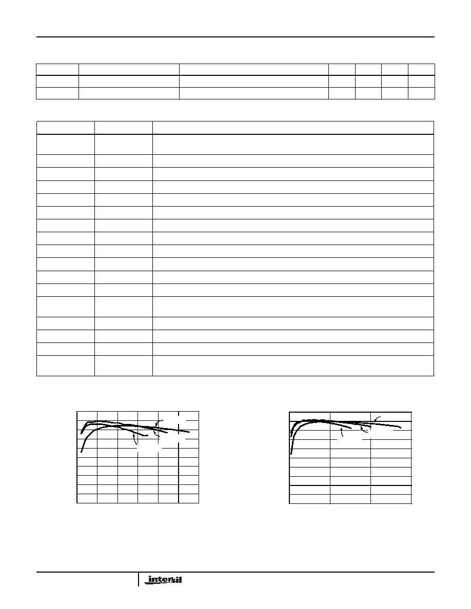
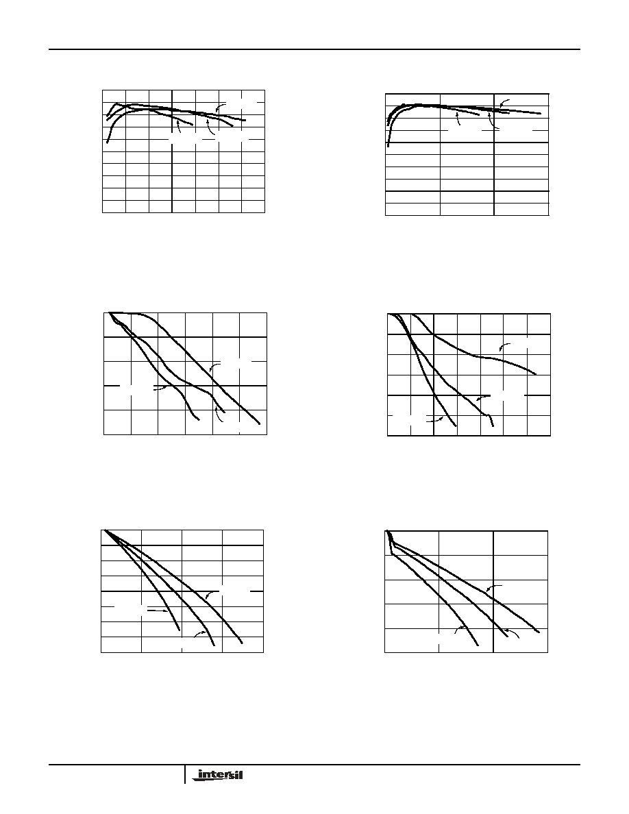
Typical Performance Curves
FIGURE 1. V
BOOST
EFFICIENCY AT V
IN
=3V (PI MODE)
FIGURE 2. V
BOOST
EFFICIENCY AT V
IN
=5V (PI MODE)
0
10
20
30
40
50
60
70
80
90
100
0
0.1
0.2
0.3
0.4
0.5
0.6
I
OUT
(A)
EFFICIENCY (%)
V
O
=9V
V
O
=12V
V
O
=15V
0
10
20
30
40
50
60
70
80
90
100
0
0.5
1
1.5
I
OUT
(A)
EFFICIENCY (%)
V
O
=9V
V
O
=12V
V
O
=15V
EL7585A
5
FN7523.2
September 21, 2005
FIGURE 3. V
BOOST
EFFICIENCY AT V
IN
=3V (P MODE)
FIGURE 4. V
BOOST
EFFICIENCY AT V
IN
=5V (P MODE)
FIGURE 5. V
BOOST
LOAD REGULATION AT V
IN
=3V (PI MODE)
FIGURE 6. V
BOOST
LOAD REGULATION AT V
IN
=5V (PI MODE)
FIGURE 7. V
BOOST
LOAD REGULATION AT V
IN
=3V (P MODE)
FIGURE 8. V
BOOST
LOAD REGULATION AT V
IN
=5V (P MODE)
Typical Performance Curves
(Continued)
0
10
20
30
40
50
60
70
80
90
100
0
0.2
0.4
0.6
0.7
I
OUT
(A)
E
F
F
I
CIENCY (%
)
0.1
0.3
0.5
V
O
=9V
V
O
=12V
V
O
=15V
0
10
20
30
40
50
60
70
80
90
100
0
0.5
1
1.5
I
OUT
(A)
EFFICIENCY (%)
V
O
=9V
V
O
=12V
V
O
=15V
-0.5
-0.4
-0.3
-0.2
-0.1
0
0
0.1
0.2
0.3
0.4
0.5
0.6
I
OUT
(A)
L
O
AD REGULA
TION (
%
)
V
O
=12V
V
O
=9V
V
O
=15V
0
0.2
0.4
0.6
0.8
1
1.2
1.4
I
OUT
(A)
LO
AD REG
U
LA
TIO
N
(%
)
V
O
=9V
V
O
=15V
-0.6
-0.5
-0.4
-0.3
-0.2
-0.1
0
V
O
=12V
-8
-7
-6
-5
-4
-3
-2
-1
0
0
0.2
0.4
0.6
0.8
I
OUT
(A)
LO
AD REG
U
LA
TIO
N
(%
)
V
O
=9V
V
O
=12V
V
O
=15V
-10
-8
-6
-4
-2
0
0
0.5
1
1.5
I
OUT
(A)
LO
AD REGU
LA
TI
ON
(%)
V
O
=9V
V
O
=12V
V
O
=15V
EL7585A
6
FN7523.2
September 21, 2005
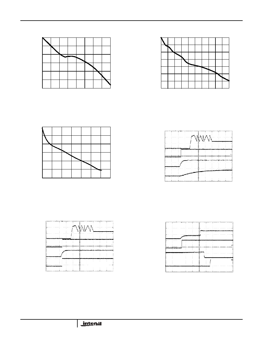
FIGURE 9. V
ON
LOAD REGULATION
FIGURE 10. V
OFF
LOAD REGULATION
FIGURE 11. V
LOGIC
LOAD REGULATION
FIGURE 12. START-UP SEQUENCE
FIGURE 13. START-UP SEQUENCE
FIGURE 14. START-UP SEQUENCE
Typical Performance Curves
(Continued)
LOAD REGULA
T
I
ON (%)
I
OUT
(mA)
0
-0.1
-0.3
-0.5
-0.6
0
20
40
60
80
-0.4
-0.2
LOAD REGULA
T
I
ON (%)
I
OUT
(mA)
0
-0.2
-0.8
-1.2
-1.4
0
20
60
80
100
-1
-0.6
40
-0.4
LO
AD REG
U
LA
TIO
N
(%
)
I
OUT
(mA)
0
-0.2
-0.6
-1
-1.2
0
100
200
500
700
-0.8
-0.4
400
300
600
V
CDLY
V
LOGIC
V
IN
EN
TIME (10ms/DIV)
C
DLY
=220nF
V
CDLY
V
LOGIC
V
IN
V
REF
TIME (10ms/DIV)
C
DLY
=220nF
TIME (10ms/DIV)
AVDD
V
LOGIC
V
OFF
V
ON
C
DLY
=220nF
EL7585A
7
FN7523.2
September 21, 2005
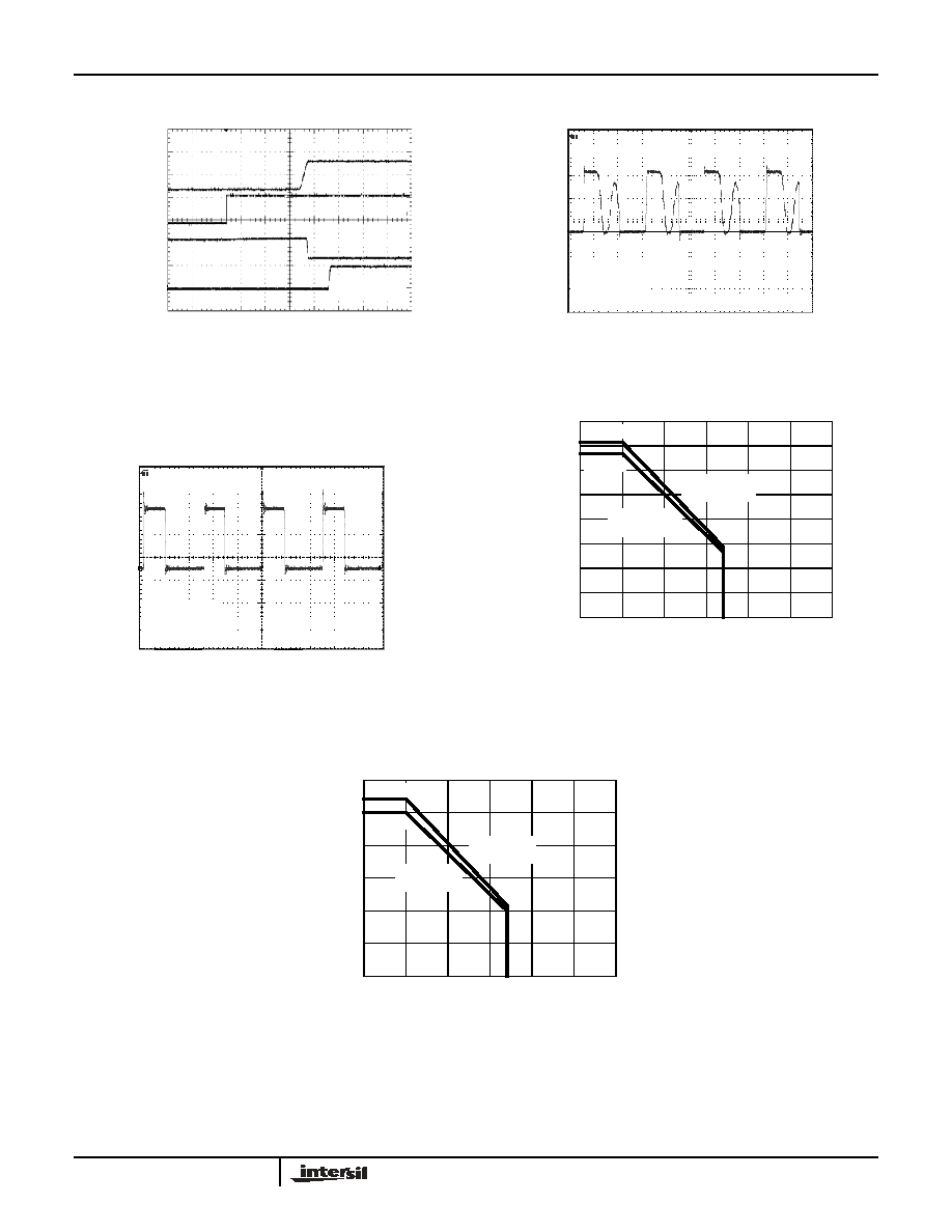
FIGURE 15. START-UP SEQUENCE
FIGURE 16. LX WAVEFORM - DISCONTINUOUS MODE
FIGURE 17. LX WAVEFORM - CONTINUOUS MODE
FIGURE 18. PACKAGE POWER DISSIPATION vs AMBIENT
TEMPERATURE
FIGURE 19. PACKAGE POWER DISSIPATION vs AMBIENT TEMPERATURE
Typical Performance Curves
(Continued)
TIME (10ms/DIV)
AVDD
V
LOGIC
V
OFF
V
ON
C
DLY
=220nF
V
IN
=5V
V
OUT
=13V
I
OUT
=30mA
TIME (400ns/DIV)
V
IN
=5V
V
OUT
=13V
I
OUT
=200mA
TIME (400ns/DIV)
JEDEC JESD51-3 AND SEMI G42-88
(SINGLE LAYER) TEST BOARD
0.8
0.7
0.5
0.3
0.2
0.1
0
0
25
50
75
100
150
AMBIENT TEMPERATURE (°C)
POWE
R
DI
SSI
PATIO
N
(
W
)
125
85
0.6
0.4
JA
=140°C/W
QFN24
JA
=150°C/W
QFN16
667mW
714mW
JEDEC JESD51-7 HIGH EFFECTIVE THERMAL
CONDUCTIVITY TEST BOARD - QFN EXPOSED
DIEPAD SOLDERED TO PCB PER JESD51-5
3
2.5
2
1.5
1
0.5
0
P
O
WER DIS
S
IPATION
(W)
2.703W
2.500W
JA
=40°C/W
QFN16
JA
=37°C/W
QFN24
0
25
50
75
100
150
AMBIENT TEMPERATURE (°C)
125
85
EL7585A
8
FN7523.2
September 21, 2005
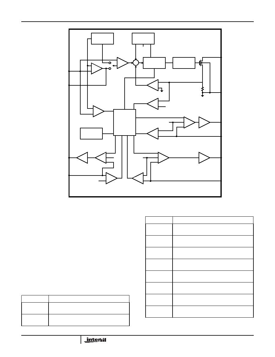
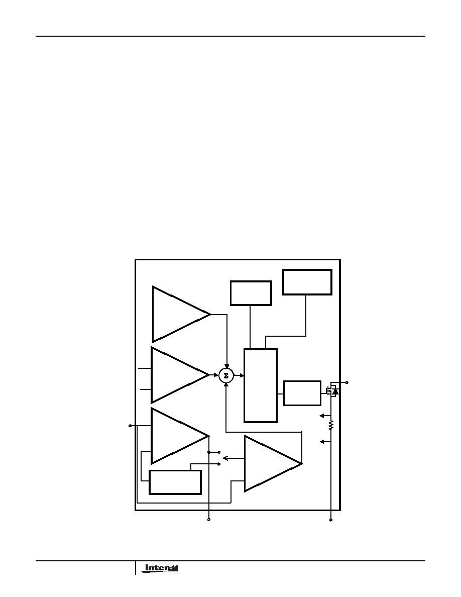
Applications Information
The EL7585A is a highly integrated multiple output power
solution for TFT-LCD applications. The system consists of
one high efficiency boost converter and three linear-
regulator controllers (V
ON
, V
OFF
, and V
LOGIC
) with multiple
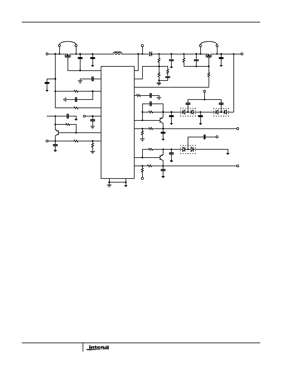
protection functions. A block diagram is shown in Figure 20.
Table 1 lists the recommended components.
The EL7585A integrates an N-channel MOSFET boost
converter to minimize external component count and cost.
The A
VDD
, V
ON
, V
OFF
, and V
LOGIC
output voltages are
independently set using external resistors. V
ON
, V
OFF
voltages require external charge pumps which are post
regulated using the integrated LDO controllers.
PWM
LOGIC
CONTROLLER
BUFFER
OSCILLATOR
SLOPE
COMPENSATION
OSC
REFERENCE
V
REF
GM
AMPLIFIER
UVLO
COMPARATOR
VOLTAGE
AMPLIFIER
CURRENT
AMPLIFIER
THERMAL
SHUTDOWN
SS
+
-
UVLO
COMPARATOR
BUFFER
UVLO
COMPARATOR
UVLO
COMPARATOR
SS
+
-
SS
+
-
BUFFER
SHUTDOWN
& START-UP
CONTROL
BUFFER
FBP
DRVL
FBL
DRVP
FBB
C
INT
DRVN
FBN
0.4V
0.2V
V
REF
V
REF
COMP
CURRENT
LIMIT COMPARATOR
CURRENT REF
PGND
LX
FIGURE 20. BLOCK DIAGRAM
TABLE 1. RECOMMENDED COMPONENTS
DESIGNATION
DESCRIPTION
C
1
, C
2
, C
3
10µF, 16V X5R ceramic capacitor (1206)
TDK C3216X5R0J106K
C
20
, C
31
4.7µF, 25V X5R ceramic capacitor (1206)
TDK C3216X5R1A475K
D
1
1A 20V low leakage Schottky rectifier (CASE 457-
04) ON SEMI MBRM120ET3
D
11
, D
12
, D
21
200mA 30V Schottky barrier diode (SOT-23)
Fairchild BAT54S
L
1
6.8µH 1.3A Inductor
TDK SLF6025T-6R8M1R3-PF
Q
1
-2.4 -20V P-channel 1.8V specified PowerTrench
MOSFET (SuperSOT-3) Fairchild FDN304P
Q
4
-2A -30V single P-channel logic level PowerTrench
MOSFET (SuperSOT-3) Fairchild FDN360P
Q
3
200mA 40V PNP amplifier (SOT-23)
Fairchild MMBT3906
Q
2
200mA 40V NPN amplifier (SOT-23)
Fairchild MMBT3904
Q
5
1A 30V PNP low saturation amplifier (SOT-23)
Fairchild FMMT549
TABLE 1. RECOMMENDED COMPONENTS (Continued)
DESIGNATION
DESCRIPTION
EL7585A
9
FN7523.2
September 21, 2005
Boost Converter
The main boost converter is a current mode PWM converter at
a fixed frequency of 1MHz which enables the use of low profile
inductors and multilayer ceramic capacitors. This results in a
compact, low cost power system for LCD panel design.
The EL7585A is designed for continuous current mode, but
they can also operate in discontinuous current mode at light
load. In continuous current mode, current flows continuously
in the inductor during the entire switching cycle in steady
state operation. The voltage conversion ratio in continuous
current mode is given by:
Where D is the duty cycle of the switching MOSFET.
Figure 21 shows the block diagram of the boost regulator. It
uses a summing amplifier architecture consisting of GM
stages for voltage feedback, current feedback and slope
compensation. A comparator looks at the peak inductor
current cycle by cycle and terminates the PWM cycle if the
current limit is reached.
An external resistor divider is required to divide the output
voltage down to the nominal reference voltage. Current
drawn by the resistor network should be limited to maintain
the overall converter efficiency. The maximum value of the
resistor network is limited by the feedback input bias current
and the potential for noise being coupled into the feedback
pin. A resistor network in the order of 60k
is recommended.
The boost converter output voltage is determined by the
following equation:
The current through the MOSFET is limited to 3.5A peak.
This restricts the maximum output current based on the
following equation:
Where
IL is peak to peak inductor ripple current, and is set by:
where f
S
is the switching frequency.
A
VDD
V
IN
----------------
1
1 D
-------------
=
A
VDD
R
1
R
2
+
R
1
--------------------- V
REF
×
=
I
OMAX
I
LMT
I
L
2
--------
V
IN
V
O
---------
×
=
I
L
V
IN
L
---------
D
f
S
-----
×
=
Iref
Iref
FBB
Ifb
Ifb
CINT
VOLTAGE
AMPLIFIER
LX
PGND
SHUTDOWN
& START-UP
CONTROL
GM
AMPLIFIER
SLOPE
COMPENSATION
BUFFER
PWM
LOGIC
CURRENT
AMPLIFIER
CLOCK
REFERENCE
GENERATOR
FIGURE 21. BLOCK DIAGRAM OF THE BOOST REGULATOR
EL7585A
10
FN7523.2
September 21, 2005
The following table gives typical values (margins are
considered 10%, 3%, 20%, 10%, and 15% on V
IN
, V
O
, L, f
S
,
and I
OMAX
:
Input Capacitor
An input capacitor is used to supply the peak charging
current to the converter. It is recommended that C
IN
be
larger than 10µF. The reflected ripple voltage will be smaller
with larger C
IN
. The voltage rating of input capacitor should
be larger than maximum input voltage.
Boost Inductor
The boost inductor is a critical part which influences the
output voltage ripple, transient response, and efficiency.
Values of 3.3µH to 10µH are to match the internal slope
compensation. The inductor must be able to handle the
following average and peak current:
Rectifier Diode
A high-speed diode is necessary due to the high switching
frequency. Schottky diodes are recommended because of
their fast recovery time and low forward voltage. The rectifier
diode must meet the output current and peak inductor
current requirements.
Output Capacitor
The output capacitor supplies the load directly and reduces
the ripple voltage at the output. Output ripple voltage
consists of two components: the voltage drop due to the
inductor ripple current flowing through the ESR of output
capacitor, and the charging and discharging of the output
capacitor.
For low ESR ceramic capacitors, the output ripple is
dominated by the charging and discharging of the output
capacitor. The voltage rating of the output capacitor should
be greater than the maximum output voltage.
NOTE: Capacitors have a voltage coefficient that makes their
effective capacitance drop as the voltage across them increases.
C
OUT
in the equation above assumes the effective value of the
capacitor at a particular voltage and not the manufacturer's stated
value, measured at zero volts.
Compensation
The EL7585A can operate in either P mode or PI mode.
Connecting the C
INT
pin directly to V
IN
will enable P mode;
For better load regulation, use PI mode with a 4.7nF
capacitor in series with a 10K resistor between C
INT
and
ground. This value may be reduced to improve transient
performance, however, very low values will reduce loop
stability.
Boost feedback resistors
As the boost output voltage, A
VDD
, is reduced below 12V the
effective voltage feedback in the IC increases the ratio of
voltage to current feedback at the summing comparator
because R
2
decreases relative to R
1
. To maintain stable
operation over the complete current range of the IC, the
voltage feedback to the FBB pin should be reduced
proportionally, as A
VDD
is reduced, by means of a series
resistor-capacitor network (R
7
and C
7
) in parallel with R
1
,
with a pole frequency (f
p
) set to approximately 10kHz for C
2
effective = 10µF and 4kHz for C
2
(effective) = 30µF.
R
7
= ((1/0.1 x R
2
) - 1/R
1
)^-1
C
7
= 1/(2 x 3.142 x f
p
x R
7
)
PI mode C
INT
(C
23
) and R
INT
(R
10
)
The IC is designed to operate with a minimum C
23
capacitor
of 4.7nF and a minimum C
2
(effective) = 10µF.
Note that, for high voltage A
VDD
, the voltage coefficient of
ceramic capacitors (C
2
) reduces their effective capacitance
greatly; a 16V 10µF ceramic can drop to around 3µF at 15V.
To improve the transient load response of A
VDD
in PI mode,
a resistor may be added in series with the C
23
capacitor. The
larger the resistor the lower the overshoot but at the expense
of stability of the converter loop - especially at high currents.
With L = 10µH, A
VDD
= 15V, C
23
= 4.7nF, C
2
(effective)
should have a capacitance of greater than 10µF. R
INT
(R
7
)
can have values up to 5k
for C
2
(effective) up to 20µF and
up to 10K for C
2
(effective) up to 30µF.
Larger values of R
INT
(R
7
) may be possible if maximum
A
VDD
load currents less than the current limit are used. To
ensure A
VDD
stability, the IC should be operated at the
maximum desired current and then the transient load
response of A
VDD
should be used to determine the
maximum value of R
INT
.
TABLE 2.
V
IN
(V)
V
O
(V)
L (µH)
f
S
(MHz)
I
OMAX
3.3
9
6.8
1
1.040686
3.3
12
6.8
1
0.719853
3.3
15
6.8
1
0.527353
5
9
6.8
1
1.576797
5
12
6.8
1
1.090686
5
15
6.8
1
0.79902
I
LAVG
I
O
1 D
-------------
=
I
LPK
I
LAVG
I
L
2
--------
+
=
V
RIPPLE
I
LPK
ESR
V
O
V
IN
V
O
------------------------
I
O
C
OUT
----------------
1
f
S
-----
×
×
+
×
=
EL7585A
11
FN7523.2
September 21, 2005
Cascaded MOSFET Application
A 20V N-channel MOSFET is integrated in the boost
regulator. For the applications where the output voltage is
greater than 20V, an external cascaded MOSFET is needed
as shown in Figure 22. The voltage rating of the external
MOSFET should be greater than V
BOOST
.
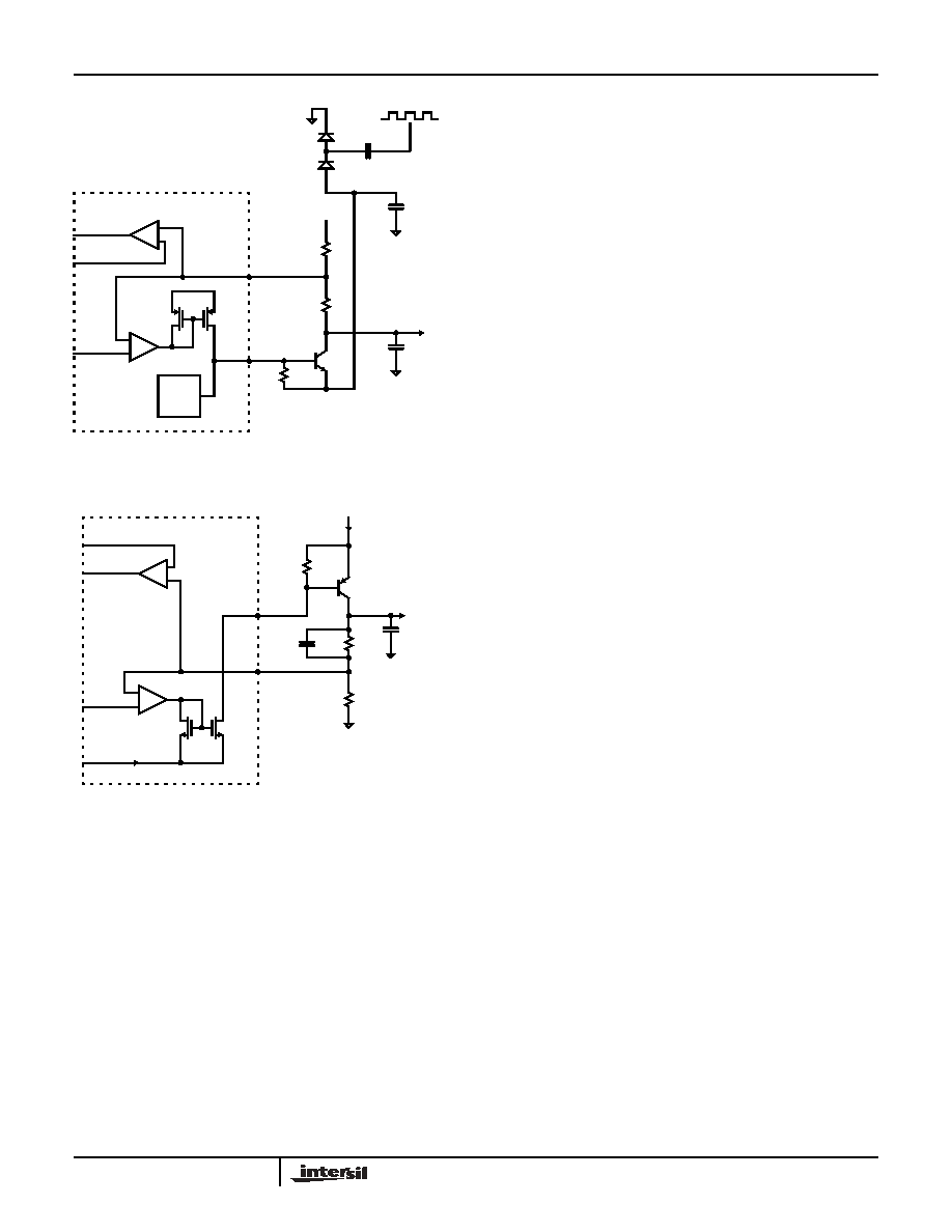
Linear-Regulator Controllers (V
ON
, V
LOGIC
, and
V
OFF
)
The EL7585A includes three independent linear-regulator
controllers, in which two are positive output voltage (V
ON
and V
LOGIC
), and one is negative. The V
ON
, V
OFF
, and
V
LOGIC
linear-regulator controller functional diagrams,
applications circuits are shown in Figures 23, 24, and 25
respectively.
Calculation of the Linear Regulator Base-Emitter
Resistors (R
BL
, R
BP
and R
BN
)
For the pass transistor of the linear regulator, low frequency
gain (Hfe) and unity gain freq. (f
T
) are usually specified in the
datasheet. The pass transistor adds a pole to the loop
transfer function at f
p
=f
T
/Hfe. Therefore, in order to maintain
phase margin at low frequency, the best choice for a pass
device is often a high frequency low gain switching
transistor. Further improvement can be obtained by adding a
base-emitter resistor R
BE
(R
BP
, R
BL
, R
BN
in the Functional
Block Diagram), which increase the pole frequency to:
f
p
=f
T
*(1+ Hfe *re/R
BE
)/Hfe, where re=KT/qIc. So choose the
lowest value R
BE
in the design as long as there is still
enough base current (I
B
) to support the maximum output
current (I
C
).
We will take as an example the V
LOGIC
linear regulator. If a
Fairchild FMMT549 PNP transistor is used as the external
pass transistor, Q5 in the application diagram, then for a
maximum V
LOGIC
operating requirement of 500mA the data
sheet indicates Hfe_min = 100.
The base-emitter saturation voltage is: Vbe_max = 1.25V
(note this is normally a Vbe ~ 0.7V, however, for the Q5
transistor an internal Darlington arrangement is used to
increase it's current gain, giving a 'base-emitter' voltage of
2 x V
BE
).
(Note that using a high current Darlington PNP transistor for
Q5 requires that V
IN
> V
LOGIC
+ 2V. Should a lower input
voltage be required, then an ordinary high gain PNP
transistor should be selected for Q5 so as to allow a lower
collector-emitter saturation voltage).
For the EL7585A, the minimum drive current is:
I_DRVL_min = 8mA
The minimum base-emitter resistor, R
BL
, can now be
calculated as:
R
BL
_min = V
BE
_max/(I_DRVL_min - Ic/Hfe_min) =
1.25V/(8mA - 500mA/100) = 417
This is the minimum value that can be used - so, we now
choose a convenient value greater than this minimum value;
say 500
. Larger values may be used to reduce quiescent
current, however, regulation may be adversely affected, by
supply noise if R
BL
is made too high in value.
EL7585A
FB
LX
V
BOOST
V
IN
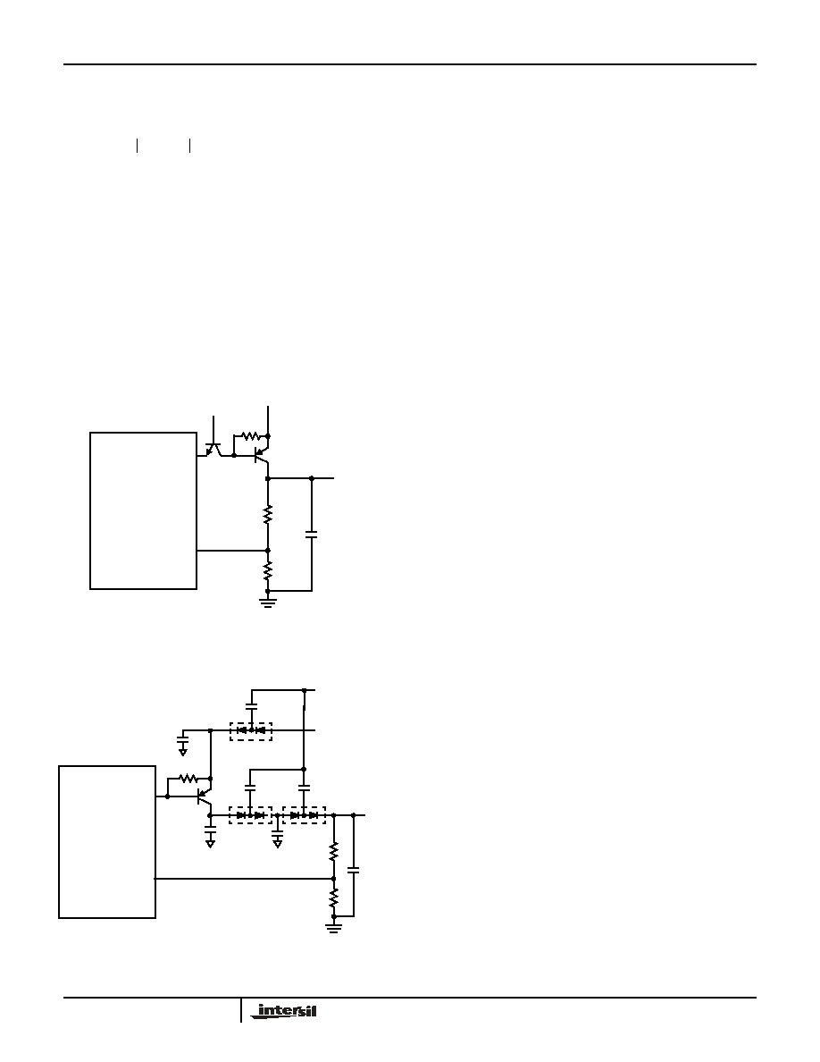
FIGURE 22. CASCADED MOSFET TOPOLOGY FOR HIGH
OUTPUT VOLTAGE APPLICATIONS
-
+
-
+
36V
ESD
CLAMP
GMP
LDO_ON
PG_LDOP
1: Np
FBP
DRVP
7k
R
BP
V
BOOST
0.1µF
0.1µF
CP (TO 36V)
20k
R
P2
R
P1
C
ON
V
ON
(TO 35V)
LX
0.9V
Q3
FIGURE 23. V
ON
FUNCTIONAL BLOCK DIAGRAM
EL7585A
12
FN7523.2
September 21, 2005
The V
ON
power supply is used to power the positive supply
of the row driver in the LCD panel. The DC-DC consists of an
external diode-capacitor charge pump powered from the
inductor (LX) of the boost converter, followed by a low
dropout linear regulator (LDO_ON). The LDO_ON regulator
uses an external PNP transistor as the pass element. The
onboard LDO controller is a wide band (>10MHz)
transconductance amplifier capable of 4mA drive current,
which is sufficient for up to 40mA or more output current
under the low dropout condition (forced beta of 10). Typical
V
ON
voltage supported by EL7585A ranges from +15V to
+36V. A fault comparator is also included for monitoring the
output voltage. The under-voltage threshold is set at 25%
below the 1.2V reference.
The V
OFF
power supply is used to power the negative
supply of the row driver in the LCD panel. The DC-DC
consists of an external diode-capacitor charge pump
powered from the inductor (LX) of the boost converter,
followed by a low dropout linear regulator (LDO_OFF). The
LDO_OFF regulator uses an external NPN transistor as the
pass element. The onboard LDO controller is a wide band
(>10MHz) transconductance amplifier capable of 4mA drive
current, which is sufficient for up to 40mA or more output
current under the low dropout condition (forced beta of 10).
Typical V
OFF
voltage supported by EL7585A ranges from
-5V to -20V. A fault comparator is also included for
monitoring the output voltage. The undervoltage threshold is
set at 200mV above the 0.2V reference level.
The V
LOGIC
power supply is used to power the logic circuitry
within the LCD panel. The DC-DC may be powered directly
from the low voltage input, 3.3V or 5.0V, or it may be
powered through the fault protection switch. The
LDO_LOGIC regulator uses an external PNP transistor as
the pass element. The onboard LDO controller is a wide
band (>10MHz) transconductance amplifier capable of
16mA drive current, which is sufficient for up to 160mA or
more output current under the low dropout condition (forced
beta of 10). Typical V
LOGIC
voltage supported by EL7585A
ranges from +1.3V to V
DD
-0.2V. A fault comparator is also
included for monitoring the output voltage. The undervoltage
threshold is set at 25% below the 1.2V reference.
Set-Up Output Voltage
Refer to the Typical Application Diagram, the output voltages
of V
ON
, V
OFF
, and V
LOGIC
are determined by the following
equations:
Where V
REF
= 1.2V, V
REFN
= 0.2V.
Resistor networks in the order of 250k
, 120k and 10k
are recommended for V
ON
, V
OFF
and V
LOGIC
, respectively.
Charge Pump
To generate an output voltage higher than V
BOOST
, single or
multiple stages of charge pumps are needed. The number of
stage is determined by the input and output voltage. For
positive charge pump stages:
where V
CE
is the dropout voltage of the pass component of
the linear regulator. It ranges from 0.3V to 1V depending on
-
+
-
+
36V
ESD
CLAMP
GMN
LDO_OFF
1: Nn
FBN
DRVN
0.1µF
0.1µF
CP (TO -26V)
R
BN
C
OFF
V
OFF
(TO -20V)
3k
LX
R
N1
R
N2
20k
V
REF
PG_LDON
0.4V
Q2
FIGURE 24. V
OFF
FUNCTIONAL BLOCK DIAGRAM
-
+
-
+
GML
LDO_LOG
PG_LDOL
1: N1
FBL
DRVL
V
IN
OR V
PROT
(3V TO 6V)
20k
R
L2
R
L1
C
LOG
V
LOGIC
(1.3V TO 3.6V)
0.9V
10µF
500
R
BL
Q5
FIGURE 25. V
LOGIC
FUNCTIONAL BLOCK DIAGRAM
V
ON
V
REF
1
R
12
R
11
----------
+
×
=
V
OFF
V
REFN
R
22
R
21
----------
V
REFN
V
REF
(
)
×
+
=
V
LOGIC
V
REF
1
R
42
R
41
----------
+
×
=
N
POSITIVE
V
OUT
V
CE
V
INPUT
+
V
INPUT
2 V
F
×
--------------------------------------------------------------
EL7585A
13
FN7523.2
September 21, 2005
the transistor. V
F
is the forward-voltage of the charge pump
rectifier diode.
The number of negative charge pump stages is given by:
To achieve high efficiency and low material cost, the lowest
number of charge pump stages which can meet the above
requirements, is always preferred.
High Charge Pump Output Voltage (>36V)
Applications
In the applications where the charge pump output voltage is
over 36V, an external npn transistor need to be inserted into
between DRVP pin and base of pass transistor Q3 as shown
in Figure 26; or the linear regulator can control only one
stage charge pump and regulate the final charge pump
output as shown in Figure 27.
Discontinuous/Continuous Boost Operation and
its Effect on the Charge Pumps
The EL7585A V
ON
and V
OFF
architecture uses LX switching
edges to drive diode charge pumps from which LDO
regulators generate the V
ON
and V
OFF
supplies. It can be
appreciated that should a regular supply of LX switching
edges be interrupted, for example during discontinuous
operation at light A
VDD
boost load currents, then this may
affect the performance of V
ON
and V
OFF
regulation -
depending on their exact loading conditions at the time.
To optimize V
ON
/V
OFF
regulation, the boundary of
discontinuous/continuous operation of the boost converter
can be adjusted, by suitable choice of inductor given V
IN
,
V
OUT
, switching frequency and the A
VDD
current loading, to
be in continuous operation.
The following equation gives the boundary between
discontinuous and continuous boost operation. For
continuous operation (LX switching every clock cycle) we
require that:
I(A
VDD
_load) > D*(1-D)*V
IN
/(2*L*F
OSC
)
where the duty cycle, D = (A
VDD
- V
IN
)/A
VDD
For example, with V
IN
= 5V, F
OSC
= 1.0MHz and A
VDD
=
12V we find continuous operation of the boost converter can
be guaranteed for:
L = 10µH and I(A
VDD
) > 61mA
L = 6.8µH and I(A
VDD
) > 89mA
L = 3.3µH and I(A
VDD
) > 184mA
Charge Pump Output Capacitors
Ceramic capacitors with low ESR are recommended. With
ceramic capacitors, the output ripple voltage is dominated by
the capacitance value. The capacitance value can be
chosen by the following equation:
where f
OSC
is the switching frequency.
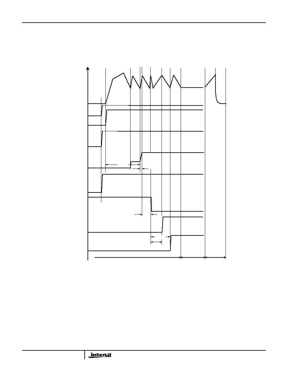
Start-Up Sequence
Figure 28 shows a detailed start-up sequence waveform. For
a successful power-up, there should be six peaks at V
CDLY
.
When a fault is detected, the device will latch off until either
EN is toggled or the input supply is recycled.
When the input voltage (V
DD
) exceeds 2.5V, V
REF
and
V
LOGIC
turn on. At the same time, if EN is tied to V
DD
, an
internal current source starts to charge C
DLY
to an upper
threshold using a fast ramp followed by a slow ramp. If EN is
low at this point, the C
DLY
ramp will be delayed until EN
goes high.
The first four ramps on C
DLY
(two up, two down) are used to
initialize the fault protection switch and to check whether
N
NEGATIVE
V
OUTPUT
V
CE
+
V
INPUT
2 V
F
×
-------------------------------------------------
V
IN
OR A
VDD
CHARGE PUMP
OUTPUT
7k
Q3
FBP
EL7585A
DRVP
NPN
CASCODE
TRANSISTOR
V
ON
FIGURE 26. CASCODE NPN TRANSISTOR CONFIGURATION
FOR HIGH CHARGE PUMP OUTPUT VOLTAGE
(>36V)
V
ON
(>36V)
0.1µF
0.1µF
0.1µF
0.1µF
7k
0.47µF
0.22µF
0.1µF
A
VDD
LX
Q3
FBP
EL7585A
DRVP
FIGURE 27. THE LINEAR REGULATOR CONTROLS ONE
STAGE OF CHARGE PUMP
C
OUT
I
OUT
2 V
RIPPLE
f
OSC
×
×
------------------------------------------------------
EL7585A

14
FN7523.2
September 21, 2005
there is a fault condition on C
DLY
or V
REF
. If a fault is
detected, the outputs and the input protection will turn off,
but V
REF
will stay on. If no fault is found, C
CDLY
continues
ramping up and down.
During the second ramp, the device checks the status of
V
REF
and over temperature. At the peak of the second ramp,
PG output goes low and enables the input protection PMOS
Q1. Q1 is a controlled FET used to prevent in-rush current into
V
BOOST
before V
BOOST
is enabled internally. Its rate of turn
on is controlled by C
o
. When a fault is detected, M1 will turn
off and disconnect the inductor from V
IN
.
With the input protection FET on, NODE1 (See Typical
Application Diagram) will rise to ~V
IN
. Initially the boost is not
enabled so V
BOOST
rises to V
IN
-V
DIODE
through the output
diode. Hence, there is a step at V
BOOST
during this part of the
start-up sequence. If this step is not desirable, an external
PMOS FET can be used to delay the output until the boost is
enabled internally. The delayed output appears at A
VDD
.
For EL7585A, V
BOOST
soft-start at the beginning of the third
ramp. The soft-start ramp depends on the value of the C
DLY
capacitor. For C
DLY
of 220nF, the soft-start time is ~2ms.
V
OFF
turns on at the start of the fourth peak. At the fifth
peak, DELB gate goes low to turn on the external PMOS Q4
to generate a delayed V
BOOST
output.
V
ON
is enabled at the beginning of the sixth ramp. A
VDD
,
PG, V
OFF
, DELB and V
ON
are checked at end of this ramp.
Fault Protection
During the startup sequence, prior to BOOST soft-start,
V
REF
is checked to be within ±20% of its final value and the
device temperature is checked. If either of these are not
within the expected range, the part is disabled until the
power is recycled or EN is toggled.
If C
DELAY
is shorted low, then the sequence will not start,
while if C
DELAY
is shorted H, the first down ramp will not
occur and the sequence will not complete.
Once the start-up sequence is completed, the chip
continuously monitors C
DLY
, DELB, FBP, FBL, FBN, V
REF
,
FBB and PG and checks for faults. During this time, the
voltage on the C
DLY
capacitor remains at 1.15V until either a
fault is detected, or the EN pin is pulled low.
A fault on C
DELAY
, V
REF
or temperature will shut down the
chip immediately. If a fault on any other output is detected,
C
DELAY
will ramp up linearly with a 5µA (typical) current to
the upper fault threshold (typically 2.4V), at which point the
chip is disabled until the power is recycled or EN is toggled.
If the fault condition is removed prior to the end of the ramp,
the voltage on the C
DLY
capacitor returns to 1.15V.
Typical fault thresholds for FBP, FBL, FBN and FBB are
included in the tables. PG and DELB fault thresholds are
typically 0.6V.
C
INT
has an internal current-limited clamp to keep the
voltage within its normal range. If C
INT
is shorted low, the
boost regulator will attempt to regulate to 0V. If C
INT
is
shorted H, the regulator switches to P mode.
If any of the regulated outputs (V
BOOST
, V
ON
, V
OFF
or
V
LOGIC
) are driven above their target levels the drive
circuitry will switch off until the output returns to its expected
value.
If V
BOOST
is excessively loaded, the current limit will
prevent damage to the chip. While in current limit, the part
acts like a current source and the regulated output will drop.
If the output drops below the fault threshold, a ramp will be
initiated on C
DELAY
and, provided that the fault is sustained,
the chip will be disabled on completion of the ramp.
In some circumstances, (depending on ambient temperature
and thermal design of the board), continuous operation at
current limit may result in the over-temperature threshold
being exceeded, which will cause the part to disable
immediately.
All I/O also have ESD protection, which in many cases will
also provide overvoltage protection, relative to either ground
or V
DD
. However, these will not generally operate unless
abs max ratings are exceeded.
Component Selection for Start-Up Sequencing and
Fault Protection
The C
REF
capacitor is typically set at 220nF and is required
to stabilize the V
REF
output. The range of C
REF
is from
22nF to 1µF and should not be more than five times the
capacitor on C
DEL
to ensure correct start-up operation.
The C
DEL
capacitor is typically 220nF and has a usable
range from 47nF minimum to several microfarads - only
limited by the leakage in the capacitor reaching µA levels.
C
DEL
should be at least 1/5 of the value of C
REF
(See
above). Note with 220nF on C
DEL
the fault time-out will be
typically 50ms and the use of a larger/smaller value will vary
this time proportionally (e.g. 1µF will give a fault time-out
period of typically 230ms).
Fault Sequencing
The EL7585A has an advanced fault detection system which
protects the IC from both adjacent pin shorts during
operation and shorts on the output supplies.
A high quality layout/design of the PCB, in respect of
grounding quality and decoupling is necessary to avoid
falsely triggering the fault detection scheme - especially
during start-up. The user is directed to the layout guidelines
and component selection sections to avoid problems during
initial evaluation and prototype PCB generation.
EL7585A
15
FN7523.2
September 21, 2005
V
CDLY
EN
V
REF
V
BOOST
V
LOGIC
V
OFF
DELAYED
V
BOOST
V
ON
PG ON
A
VD
D
SO
FT-S
TA
RT
V
OF
F
ON
DELB ON
V
ON
SO
FT-ST
ART
FAU
LT DETECTED
CHIP
DISABLED
NORMAL
O
PERA
T
IO
N
F
AUL
T
PRESE
NT
START-UP SEQUENCE
TIMED BY C
DLY
V
REF
, V
LOG
I
C
ON
t
OS
t
ON
t
DEL1
FIGURE 28. START-UP SEQUENCE
V
IN
t
DEL3
t
DEL2
EL7585A
16
FN7523.2
September 21, 2005
Over-Temperature Protection
An internal temperature sensor continuously monitors the
die temperature. In the event that the die temperature
exceeds the thermal trip point of 140°C, the device will shut
down.
Layout Recommendation
The device's performance including efficiency, output noise,
transient response and control loop stability is dramatically
affected by the PCB layout. PCB layout is critical, especially
at high switching frequency.
There are some general guidelines for layout:
1. Place the external power components (the input
capacitors, output capacitors, boost inductor and output
diodes, etc.) in close proximity to the device. Traces to
these components should be kept as short and wide as
possible to minimize parasitic inductance and resistance.
2. Place V
REF
and V
DD
bypass capacitors close to the pins.
3. Minimize the length of traces carrying fast signals and
high current.
4. All feedback networks should sense the output voltage
directly from the point of load, and be as far away from LX
node as possible.
5. The power ground (PGND) and signal ground (SGND)
pins should be connected at only one point near the main
decoupling capacitors.
6. The exposed die plate, on the underneath of the
package, should be soldered to an equivalent area of
metal on the PCB. This contact area should have multiple
via connections to the back of the PCB as well as
connections to intermediate PCB layers, if available, to
maximize thermal dissipation away from the IC.
7. To minimize the thermal resistance of the package when
soldered to a multi-layer PCB, the amount of copper track
and ground plane area connected to the exposed die
plate should be maximized and spread out as far as
possible from the IC. The bottom and top PCB areas
especially should be maximized to allow thermal
dissipation to the surrounding air.
8. A signal ground plane, separate from the power ground
plane and connected to the power ground pins only at the
exposed die plate, should be used for ground return
connections for feedback resistor networks (R
1
, R
11
,
R
41
) and the V
REF
capacitor, C
22
, the C
DELAY
capacitor
C
7
and the integrator capacitor C
23
.
9. Minimize feedback input track lengths to avoid switching
noise pick-up.
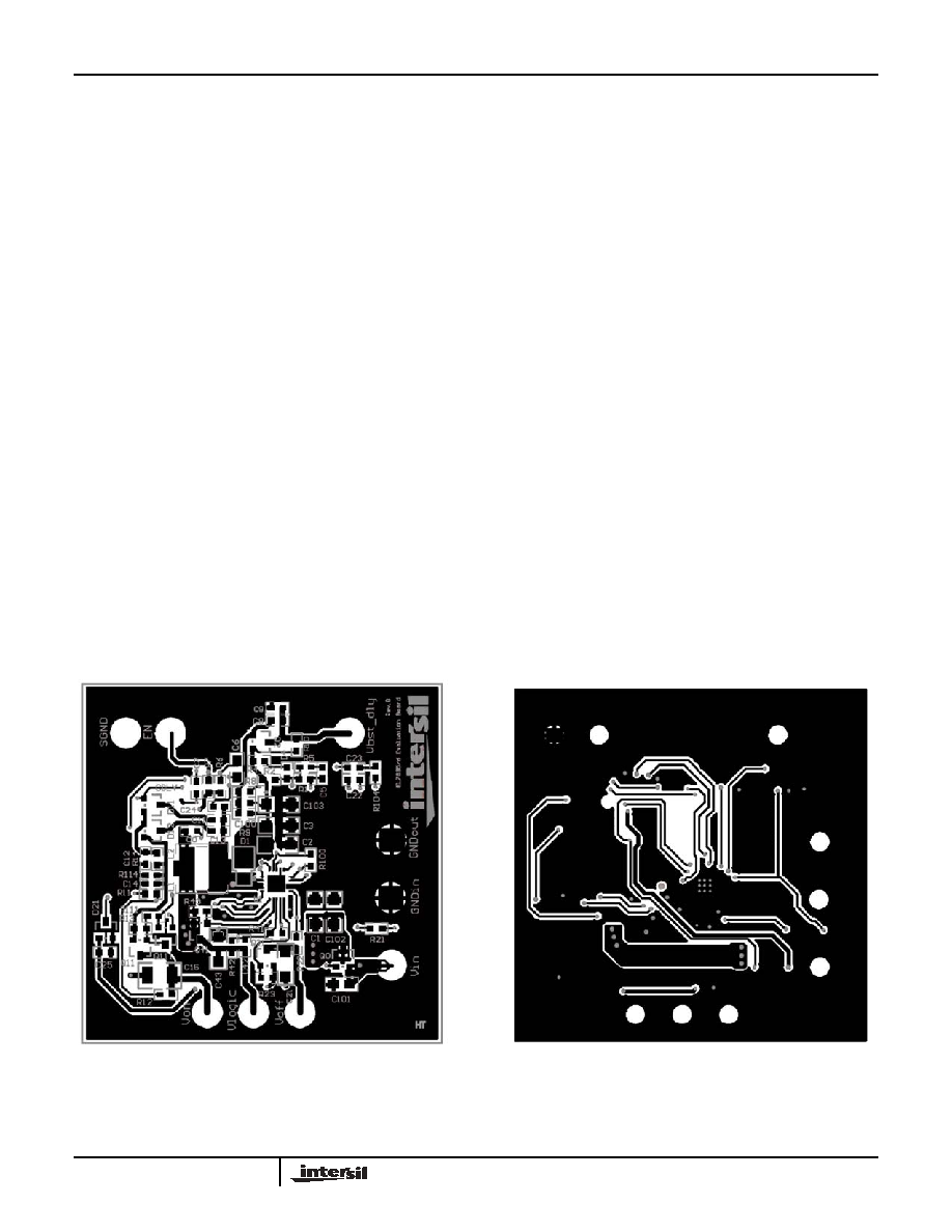
A two-layer demo board is available to illustrate the proper
layout implementation. A four-layer demo board can be used
to further optimize the layout recommendations.
Demo Board Layout
FIGURE 29. TOP LAYER
FIGURE 30. BOTTOM LAYER
EL7585A
17
FN7523.2
September 21, 2005
Typical Application Diagram
NOTE: The SGND should be connected to the exposed die plate and connected to the PGND at one point only.
LX
FBB
DELB
CINT
DRVP
FBP
DRVN
FBN
PGND
PG
CDELAY
VDD
EN
VREF
DRVL
FBL
SGND
V
IN
C
10
4.7µF
NODE 1
V
LOGIC
(2.5V) C
31
4.7µF
C
41
0.1µF
R
43
500
C
22
0.1µF
R
42
5.4k
R
41
5k
R
7
10k
V
REF
C
6
4.7µF
R
6
10
C
7
0.22µF
Q
1
C
0
1nF
C
1
10µF
x2
NODE 1
L
1
6.8µH
LX
D
1
R
2
46.5k
R
1
5k
C
2
10µF
R
9
1M
C
16
22nF
C
9
0.1µF
R
8
10k
A
VDD
(12V)
C
23
4.7nF
C
P
1nF
R
13
7k
Q
3
C
14
0.1µF
C
15
0.47µF
R
11
20k
R
12
230k
R
23
3k
R
22
104K
C
20
4.7µF
R
21
20K
C
25
0.1µF D
21
C
12
0.1µF
D
12
D
11
C
24
0.1µF
Q
2
C
13
0.1µF
C
11
0.1µF
V
ON
(15V)
V
OFF
(-5V)
LX
LX
V
REF
Q
5
Q
4
X2
R
7
OPEN
C
7
OPEN
R
10
10k
EL7585A
18
All Intersil U.S. products are manufactured, assembled and tested utilizing ISO9000 quality systems.
Intersil Corporation's quality certifications can be viewed at www.intersil.com/design/quality
Intersil products are sold by description only. Intersil Corporation reserves the right to make changes in circuit design, software and/or specifications at any time without
notice. Accordingly, the reader is cautioned to verify that data sheets are current before placing orders. Information furnished by Intersil is believed to be accurate and
reliable. However, no responsibility is assumed by Intersil or its subsidiaries for its use; nor for any infringements of patents or other rights of third parties which may result
from its use. No license is granted by implication or otherwise under any patent or patent rights of Intersil or its subsidiaries.
For information regarding Intersil Corporation and its products, see www.intersil.com
FN7523.2
September 21, 2005
EL7585A
QFN Package Outline Drawing
NOTE: The package drawing shown here may not be the latest version. To check the latest revision, please refer to the Intersil website at
http://www.intersil.com/design/packages/index.asp