1
Æ
FN9210.1
EL7586, EL7586A
TFT-LCD Power Supply
The EL7586 and EL7586A represent multiple output
regulators for use in all large panel, TFT-LCD applications.
Both feature a single boost converter with an integrated 2A
FET, two positive LDOs for V
ON
and V
LOGIC
generation,
and a single negative LDO for V
OFF
generation. The boost
converter can be programmed to operate in either P-mode
or PI-mode for improved load regulation.
Both EL7586 and EL7586A also integrate fault protection for
all four channels. Once a fault is detected, the device is
latched off until the input supply or EN is cycled. EL7586
also features an integrated start-up sequence for
V
BOOST
/V
LOGIC,
V
OFF
, then V
ON
or for V
LOGIC
, V
OFF
,
V
BOOST
, and V
ON
. The latter requires a single external
transistor. The timing of the start-up sequence is set using
an external capacitor.
EL7586A features an immediately-enabled V
LOGIC
output
which is independent of EN input. The V
LOGIC
output will be
switched off if a fault is detected and the power supply needs
to be recycled to reset this condition.
Both the EL7586 and EL7586A are pin-compatible, come in
the 20 Ld 4x4 QFN package, and are specified for operation
over the -40∞C to +85∞C temperature range.
Features
∑ 2A current limit FET options
∑ 3V to 5V input
∑ Up to 20V boost out
∑ 1% regulation on all outputs
∑ V
LOGIC
-V
OFF
-V
BOOST
-V
ON
or
V
BOOST
/V
LOGIC
-V
OFF
-V
ON
sequence control
- V
LOGIC
is on from start-up for EL7586A
∑ Programmable sequence delay
∑ Fully fault protected
∑ Thermal shutdown
∑ Internal soft-start
∑ 20 Ld 4x4 QFN packages
∑ Pb-free plus anneal available (RoHS compliant)
Applications
∑ LCD monitors (15"+)
∑ LCD-TV (up to 40"+)
∑ Notebook displays (up to 16")
∑ Industrial/medical LCD displays
Ordering Information
PART NUMBER
PART
MARKING
TAPE &
REEL
PACKAGE
PKG.
DWG. #
EL7586ILZ
(Note)
7586ILZ
-
20 Ld 4x4 QFN
(Pb-free)
MDP0046
EL7586ILZ-T7
(Note)
7586ILZ
7"
20 Ld 4x4 QFN
(Pb-free)
MDP0046
EL7586ILZ-T13
(Note)
7586ILZ
13"
20 Ld 4x4 QFN
(Pb-free)
MDP0046
EL7586AILZ
(Note)
7586AIL Z
-
20 Ld 4x4 QFN
(Pb-free)
MDP0046
EL7586AILZ-T7
(Note)
7586AIL Z
7"
20 Ld 4x4 QFN
(Pb-free)
MDP0046
EL7586AILZ-T13
(Note)
7586AIL Z
13"
20 Ld 4x4 QFN
(Pb-free)
MDP0046
NOTE: Intersil Pb-free plus anneal products employ special Pb-free
material sets; molding compounds/die attach materials and 100%
matte tin plate termination finish, which are RoHS compliant and
compatible with both SnPb and Pb-free soldering operations. Intersil
Pb-free products are MSL classified at Pb-free peak reflow
temperatures that meet or exceed the Pb-free requirements of
IPC/JEDEC J STD-020.
Pinout
EL7586, EL7586A
(20 LD 4X4 QFN)
TOP VIEW
1
2
3
4
15
14
13
12
6
7
8
9
20
19
18
17
CDLY
DELB
LX1
LX2
FBP
DR
V
L
FBL
SG
ND
PG
VD
D
EN
SG
N
D
CINT
VREF
PGND
PGND
THERMAL
PAD
5
DRVP
10
DR
V
N
11 FBN
16
FBB
Data Sheet
October 7, 2005
CAUTION: These devices are sensitive to electrostatic discharge; follow proper IC Handling Procedures.
1-888-INTERSIL or 1-888-468-3774
|
Intersil (and design) is a registered trademark of Intersil Americas Inc.
Copyright Intersil Americas Inc. 2005. All Rights Reserved
All other trademarks mentioned are the property of their respective owners.
2
FN9210.1
October 7, 2005
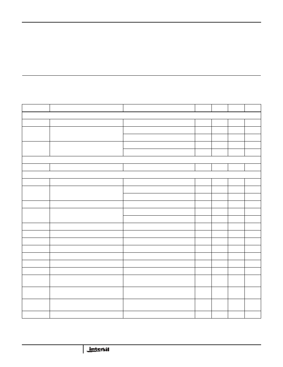
Absolute Maximum Ratings
(T
A
= 25∞C)
V
DELB
. . . . . . . . . . . . . . . . . . . . . . . . . . . . . . . . . . . . . . . . . . . . .24V
V
DRVP
. . . . . . . . . . . . . . . . . . . . . . . . . . . . . . . . . . . . . . . . . . . . .36V
V
DRVN
. . . . . . . . . . . . . . . . . . . . . . . . . . . . . . . . . . . . . . . . . . . . -20V
V
DD
. . . . . . . . . . . . . . . . . . . . . . . . . . . . . . . . . . . . . . . . . . . . . . 6.5V
V
LX
. . . . . . . . . . . . . . . . . . . . . . . . . . . . . . . . . . . . . . . . . . . . . . . .24V
V
DRVL
. . . . . . . . . . . . . . . . . . . . . . . . . . . . . . . . . . . . . . . . . . . . 6.5V
Storage Temperature . . . . . . . . . . . . . . . . . . . . . . . .-65∞C to +150∞C
Ambient Operating Temperature . . . . . . . . . . . . . . . .-40∞C to +85∞C
Power Dissipation . . . . . . . . . . . . . . . . . . . . . . . . . . . . . See Curves
Maximum Continuous Junction Temperature . . . . . . . . . . . . 125∞C
CAUTION: Stresses above those listed in "Absolute Maximum Ratings" may cause permanent damage to the device. This is a stress only rating and operation of the
device at these or any other conditions above those indicated in the operational sections of this specification is not implied.
IMPORTANT NOTE: All parameters having Min/Max specifications are guaranteed. Typical values are for information purposes only. Unless otherwise noted, all tests
are at the specified temperature and are pulsed tests, therefore: T
J
= T
C
= T
A
Electrical Specifications
V
DD
= 5V, V
BOOST
= 11V, I
LOAD
= 200mA, V
ON
= 15V, V
OFF
= -5V, V
LOGIC
= 2.5V, over temperature from
-40∞C to 85∞C, unless otherwise specified.
PARAMETER
DESCRIPTION
CONDITION
MIN
TYP
MAX
UNIT
SUPPLY
V
S
Supply Voltage
3
5.5
V
I
S
Quiescent
Current
(EL7586A)
Enabled, LX not switching
1.7
2.5
mA
Disabled
750
900
µA
I
S
Quiescent
Current
(EL7586)
Enabled, LX not switching
1.7
2.5
mA
Disabled
10
20
µA
CLOCK
F
OSC
Oscillator Frequency
900
1000
1100
kHz
BOOST
V
BOOST
Boost Output Range
5.5
20
V
V
FBB
Boost Feedback Voltage
T
A
= 25∞C
1.192
1.205
1.218
V
1.188
1.205
1.222
V
V
F_FBB
FBB Fault Trip Point
0.9
V
V
REF
Reference Voltage
T
A
= 25∞C
1.19
1.215
1.235
V
1.187
1.215
1.238
V
C
REF
V
REF
Capacitor
22
100
nF
D
MAX
Maximum Duty Cycle
85
%
I
LXMAX
Current Switch
2.0
A
I
LEAK
Switch Leakage Current
V
LX
= 16V
10
µA
r
DS(ON
Switch On-Resistance
320
m
Eff
Boost Efficiency
See curves
85
92
%
I(V
FBB
)
Feedback Input Bias Current
Pl mode, V
FBB
= 1.35V
50
500
nA
V
BOOST
/
V
IN
Line Regulation
C
INT
= 4.7nF, I
OUT
= 100mA, V
IN
= 3V to
5.5V
0.05
%/V
V
BOOST
/
I
BOOST
Load Regulation - "P" Mode
C
INT
pin strapped to V
DD
,
50mA < I
LOAD
< 250mA
3
%
V
BOOST
/
I
BOOST
Load Regulation - "PI" Mode
C
INT
= 4.7nF, 50mA < I
O
< 250mA
0.1
%
V
CINT_T
CINT Pl Mode Select Threshold
4.7
4.8
V
EL7586, EL7586A
3
FN9210.1
October 7, 2005
V
ON
LDO
V
FBP
FBP Regulation Voltage
I
DRVP
= 0.2mA, T
A
= 25∞C
1.176
1.2
1.224
V
I
DRVP
= 0.2mA
1.172
1.2
1.228
V
V
F_FBP
FBP Fault Trip Point
V
FBP
falling
0.82
0.87
0.92
V
I
FBP
FBP Input Bias Current
V
FBP
= 1.35V
-250
250
nA
GMP
FBP Effective Transconductance
V
DRVP
= 25V, I
DRVP
= 0.2 to 2mA
50
ms
V
ON
/
I(V
ON
) V
ON
Load Regulation
I(V
ON
) = 0mA to 20mA
-0.5
%
I
DRVP
DRVP Sink Current Max
V
FBP
= 1.1V, V
DRVP
= 25V
2
4
mA
I
L_DRVP
DRVP Leakage Current
V
FBP
= 1.5V, V
DRVP
= 35V
0.1
5
µA
V
OFF
LDO
V
FBN
FBN Regulation Voltage
I
DRVN
= 0.2mA, T
A
= 25∞C
0.173
0.203
0.233
V
I
DRVN
= 0.2mA
0.171
0.203
0.235
V
V
F_FBN
FNN Fault Trip Point
V
FBN
falling
0.38
0.43
0.48
V
I
FBN
FBN Input Bias Current
V
FBN
= 0.2V
-250
250
nA
GMN
FBN Effective Transconductance
V
DRVN
= -6V, I
DRVN
= 0.2mA to 2mA
50
ms
V
OFF
/
I(V
OFF
)
V
OFF
Load Regulation
I(V
OFF
) = 0mA to 20mA
-0.5
%
I
DRVN
DRVN Source Current Max
V
FBN
= 0.3V, V
DRVN
= -6V
2
4
mA
I
L_DRVN
DRVN Leakage Current
V
FBN
= 0V, V
DRVN
= -20V
0.1
5
µA
V
LOGIC
LDO
V
FBL
FBL Regulation Voltage
I
DRVL
= 1mA, T
A
= 25∞C
1.176
1.2
1.224
V
I
DRVL
= 1mA
1.174
1.2
1.226
V
V
F_FBL
FBL Fault Trip Point
V
FBL
falling
0.82
0.87
0.92
V
I
FBL
FBL Input Bias Current
V
FBL
= 1.35V
-500
500
nA
G
ML
FBL Effective Transconductance
V
DRVL
= 2.5V, I
DRVL
= 1mA to 8mA
200
ms
V
LOGIC
/
I(V
LOGIC
)
V
LOGIC
Load Regulation
I(V
LOGIC
) = 100mA to 500mA
0.5
%
I
DRVL
DRVL Sink Current Max
V
FBL
= 1.1V, V
DRVL
= 2.5V
8
16
mA
I
L_DRL
I
L_DRVL
V
FBL
= 1.5V, V
DRVL
= 5.5V
0.1
5
µA
SEQUENCING
t
ON
Turn On Delay
C
DLY
= 0.22µF
30
ms
t
SS
Soft-start Time
C
DLY
= 0.22µF
2
ms
t
DEL1
Delay Between A
VDD
and V
OFF
C
DLY
= 0.22µF
10
ms
t
DEL2
Delay Between V
ON
and V
OFF
C
DLY
= 0.22µF
17
ms
I
DELB
DELB Pull-down Current
V
DELB
> 0.6V
50
µA
V
DELB
< 0.6V
1.4
mA
C
DEL
Delay Capacitor
10
220
nF
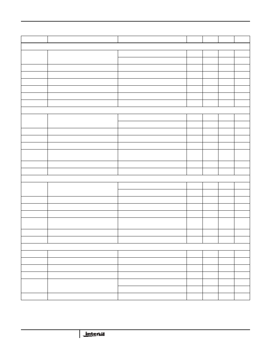
Electrical Specifications
V
DD
= 5V, V
BOOST
= 11V, I
LOAD
= 200mA, V
ON
= 15V, V
OFF
= -5V, V
LOGIC
= 2.5V, over temperature from
-40∞C to 85∞C, unless otherwise specified. (Continued)
PARAMETER
DESCRIPTION
CONDITION
MIN
TYP
MAX
UNIT
EL7586, EL7586A
4
FN9210.1
October 7, 2005
FAULT DETECTION
t
FAULT
Fault Time Out
C
DLY
= 0.22µF
50
ms
OT
Over-temperature Threshold
140
∞C
I
PG
PG Pull-down Current
VPG > 0.6V
15
µA
VPG < 0.6V
1.7
mA
LOGIC ENABLE
V
HI
Logic High Threshold
2.3
V
V
LO
Logic Low Threshold
0.8
V
I
LOW
Logic Low Bias Current
0.2
2
µA
I
HIGH
Logic High Bias Current
at V
EN
= 5V
12
18
24
µA
Electrical Specifications
V
DD
= 5V, V
BOOST
= 11V, I
LOAD
= 200mA, V
ON
= 15V, V
OFF
= -5V, V
LOGIC
= 2.5V, over temperature from
-40∞C to 85∞C, unless otherwise specified. (Continued)
PARAMETER
DESCRIPTION
CONDITION
MIN
TYP
MAX
UNIT
Pin Descriptions
PIN NAME
PIN NUMBER
DESCRIPTION
1
CDLY
A capacitor connected from this pin to GND sets the delay time for start-up sequence and sets the fault
timeout time
2
DELB
Gate drive of optional V
BOOST
delay FET
3, 4
LX1, LX2
Drain of the internal N channel boost FET; for EL7586, pin 4 is not connected
5
DRVP
Positive LDO base drive; open drain of an internal N channel FET
6
FBP
Positive LDO voltage feedback input pin; regulates to 1.2V nominal
7
DRVL
Logic LDO base drive; open drain of an internal N channel FET
8
FBL
Logic LDO voltage feedback input pin; regulates to 1.2V nominal
9, 17
SGND
Low noise signal ground
10
DRVN
Negative LDO base drive; open drain of an internal P channel FET
11
FBN
Negative LDO voltage feedback input pin; regulates to 0.2V nominal
12, 13
PGND
Power ground, connected to source of internal N channel boost FET
14
VREF
Bandgap voltage bypass, connect a 0.1µF to SGND
15
CINT
V
BOOST
integrator output, connect capacitor to SGND for PI mode or connect to V
DD
for P mode
operation
16
FBB
Boost regulator voltage feedback input pin; regulates to 1.2V nominal
18
EN
Enable pin, High = Enable; Low or floating = Disable
19
VDD
Positive supply
20
PG
Gate drive of optional fault protection FET, when chip is disabled or when a fault has been detected, this
is high
EL7586, EL7586A
5
FN9210.1
October 7, 2005
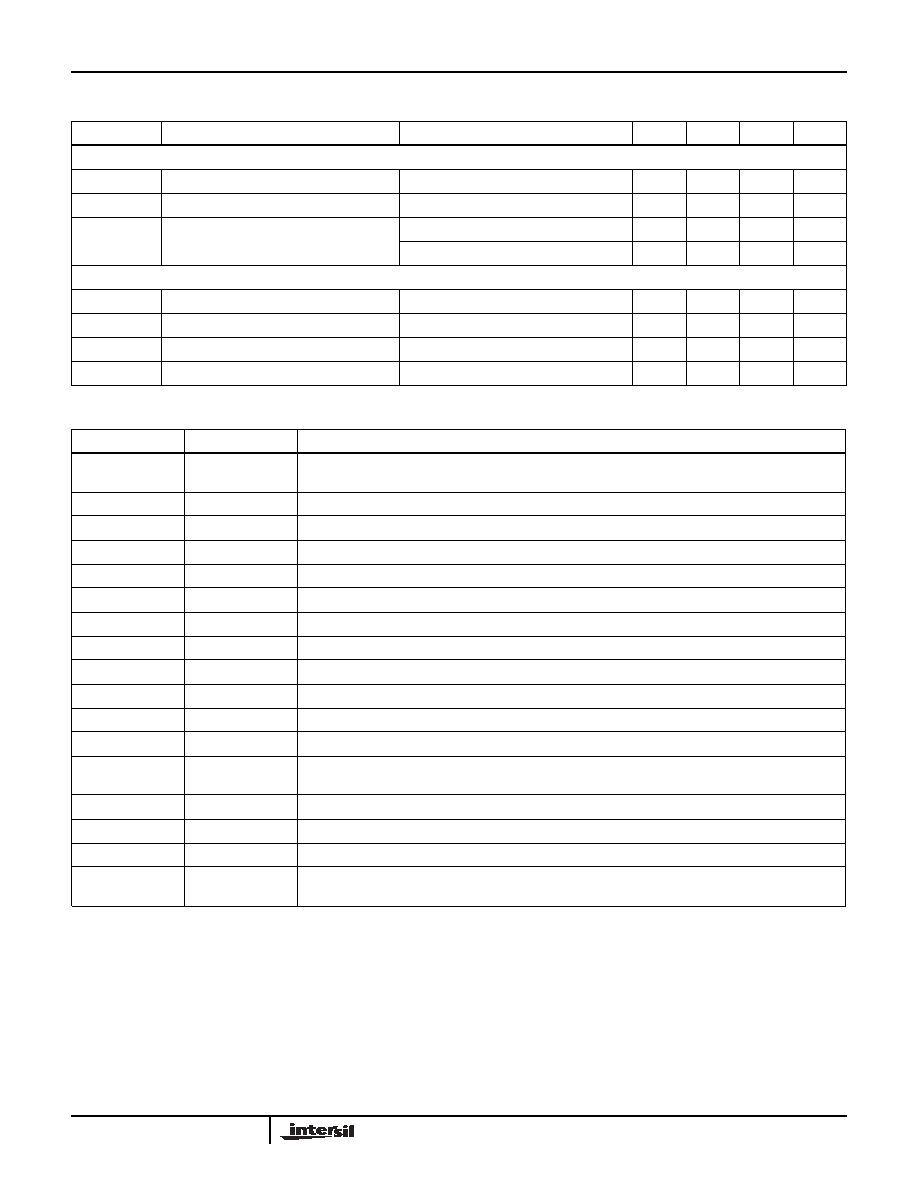
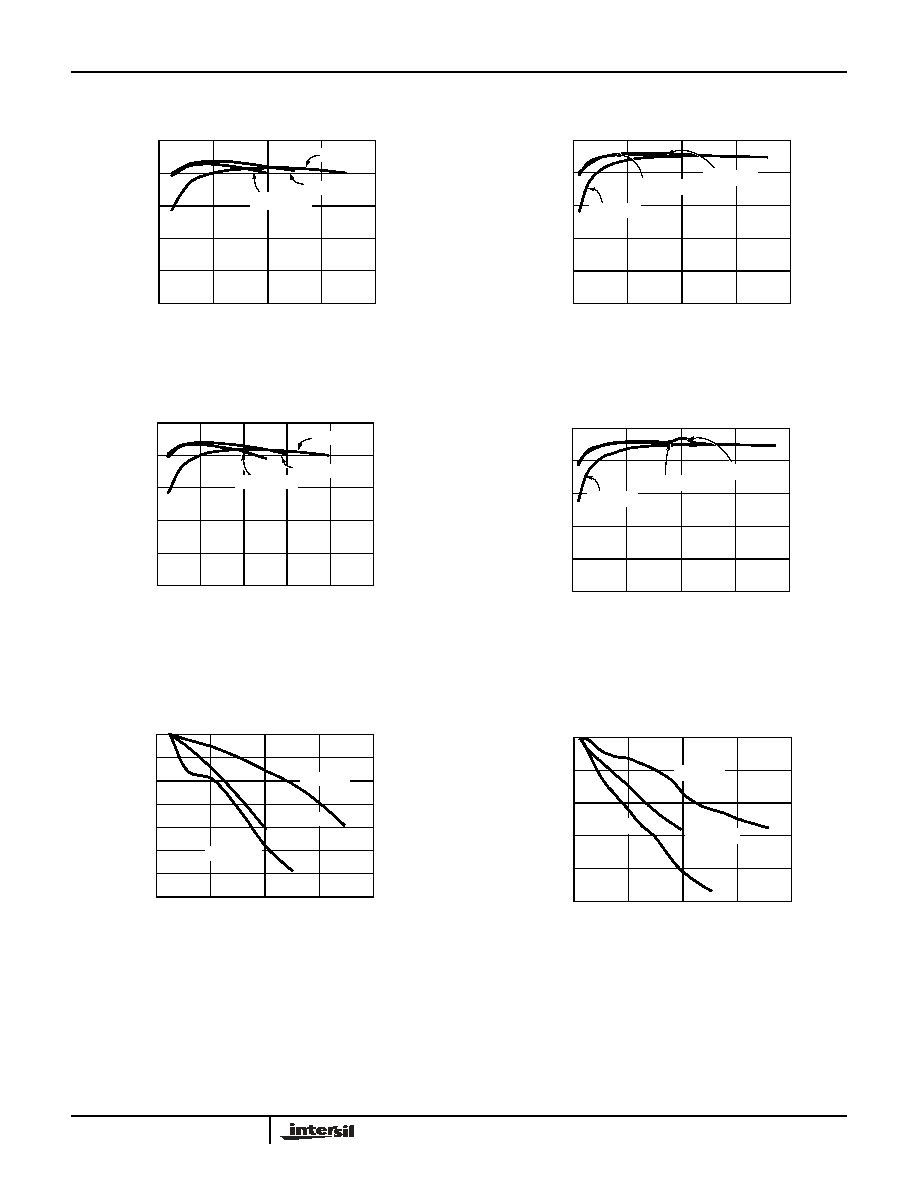
Typical Performance Curves
FIGURE 1. V
BOOST
EFFICIENCY AT V
IN
= 3V (PI MODE)
FIGURE 2. V
BOOST
EFFICIENCY AT V
IN
= 5V (PI MODE)
FIGURE 3. V
BOOST
EFFICIENCY AT V
IN
= 3V (P MODE)
FIGURE 4. V
BOOST
EFFICIENCY AT V
IN
= 5V (P MODE)
FIGURE 5. V
BOOST
LOAD REGULATION AT V
IN
= 3V (PI MODE)
FIGURE 6. V
BOOST
LOAD REGULATION AT V
IN
= 5V (PI MODE)
I
OUT
(mA)
E
F
FICIE
NCY (
%
)
A
VDD
=9V
A
VDD
=12V
0
100
200
300
400
100
80
60
40
20
0
A
VDD
=15V
0
20
40
60
80
100
0
200
400
600
800
I
OUT
(mA)
EF
FIC
I
EN
C
Y
(%
)
A
VDD
=12V
A
VDD
=9V
A
VDD
=15V
0
20
40
60
80
100
0
100
200
300
400
500
I
OUT
(mA)
EFF
I
CIENCY (%
)
A
VDD
=9V
A
VDD
=12V
A
VDD
=15V
0
20
40
60
80
100
0
200
400
600
800
I
OUT
(mA)
EFF
I
CIENCY (%
)
A
VDD
=12V
A
VDD
=9V
A
VDD
=15V
-0.7
-0.6
-0.5
-0.4
-0.3
-0.2
-0.1
0
0
100
200
300
400
I
OUT
(mA)
LO
AD R
E
G
U
LA
TIO
N
(%
)
A
VDD
=9V
A
VDD
=15V
A
VDD
=12V
0
200
400
600
800
I
OUT
(mA)
A
VDD
=12V
A
VDD
=9V
A
VDD
=15V
-1
-0.8
-0.6
-0.4
-0.2
0
LOAD REGULA
T
I
ON (%)
EL7586, EL7586A