
1
Æ
FN7415.1
EL7640, EL7641, EL7642
TFT-LCD DC/DC with Integrated
Amplifiers
The EL7640, EL7641, and EL7642 integrate a high
performance boost regulator with 2 LDO controllers for V
ON
and V
OFF
, a V
ON
-slice circuit with adjustable delay and
either one (EL7640), three (EL7641), or five amplifiers
(EL7642) for V
COM
and V
GAMMA
applications.
The boost converter in the EL7640, EL7641, and EL7642 is
a current mode PWM type integrating an 18V N-channel
MOSFET. Operating at 1.2MHz, this boost can operate in
either P-mode for superior transient response, or in PI-mode
for tighter output regulation.
Using external low-cost transistors, the LDO controllers
provide tight regulation for V
ON
, V
OFF
, as well as providing
start-up sequence control and fault protection.
The amplifiers are ideal for V
COM
and V
GAMMA
applications, with 150mA peak output current drive, 12MHz
bandwidth, and 12V/
µs slew rate. All inputs and outputs are
rail-to-rail.
Available in the 32 Ld thin QFN (5mm x 5mm) Pb-free
packages, the EL7640, EL7641, and EL7642 are specified
for operation over the -40∞C to +85∞C temperature range.
Features
∑ Current mode boost regulator
- Fast transient response
- 1% accurate output voltage
- 18V/3A integrated FET
- >90% efficiency
∑ 2.6V to 5.5V V
IN
supply
∑ 2 LDO controllers for V
ON
and V
OFF
- 2% output regulation
- V
ON
-slice circuit
∑ High speed amplifiers
- 150mA short-circuit output current
- 12V/
µs slew rate
- 12MHz -3dB bandwidth
- Rail-to-rail inputs and outputs
∑ Built-in power sequencing
∑ Internal soft-start
∑ Multiple overload protection
∑ Thermal shutdown
∑ 32 Ld 5x5 thin QFN package
∑ Pb-Free plus anneal available (RoHS compliant)
Applications
∑ TFT-LCD panels
∑ LCD monitors
∑ Notebooks
∑ LCD-TVs
Ordering Information
PART NUMBER
(Note)
PART
MARKING
TAPE &
REEL
PACKAGE
(Pb-Free)
PKG.
DWG. #
EL7640ILTZ
7640ILTZ
-
32 Ld 5x5
Thin QFN
MDP0051
EL7640ILTZ-T7
7640ILTZ
7"
32 Ld 5x5
Thin QFN
MDP0051
EL7640ILTZ-T13
7640ILTZ
13"
32 Ld 5x5
Thin QFN
MDP0051
EL7641ILTZ
7641ILTZ
-
32 Ld 5x5
Thin QFN
MDP0051
EL7641ILTZ-T7
7641ILTZ
7"
32 Ld 5x5
Thin QFN
MDP0051
EL7641ILTZ-T13
7641ILTZ
13"
32 Ld 5x5
Thin QFN
MDP0051
EL7642ILTZ
7642ILTZ
-
32 Ld 5x5
Thin QFN
MDP0051
EL7642ILTZ-T7
7642ILTZ
7"
32 Ld 5x5
Thin QFN
MDP0051
EL7642ILTZ-T13
7642ILTZ
13"
32 Ld 5x5
Thin QFN
MDP0051
NOTE: Intersil Pb-free plus anneal products employ special Pb-free material
sets; molding compounds/die attach materials and 100% matte tin plate
termination finish, which are RoHS compliant and compatible with both SnPb
and Pb-free soldering operations. Intersil Pb-free products are MSL classified at
Pb-free peak reflow temperatures that meet or exceed the Pb-free requirements
of IPC/JEDEC J STD-020.
Data Sheet
September 26, 2005
CAUTION: These devices are sensitive to electrostatic discharge; follow proper IC Handling Procedures.
1-888-INTERSIL or 1-888-468-3774
|
Intersil (and design) is a registered trademark of Intersil Americas Inc.
Copyright Intersil Americas Inc. 2005. All Rights Reserved
All other trademarks mentioned are the property of their respective owners.
2
FN7415.1
September 26, 2005
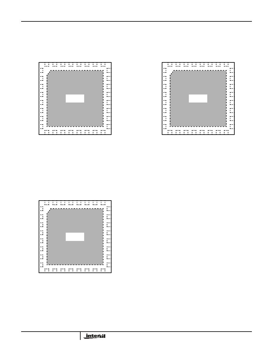
Pinouts
EL7640
(32 LD QFN)
TOP VIEW
EL7641
(32 LD QFN)
TOP VIEW
EL7642
(32 LD QFN)
TOP VIEW
NC = NOT INTERNALLY CONNECTED
IC = INTERNALLY CONNECTED
THERMAL
PAD
24
23
22
21
20
19
18
32
31
30
29
28
10
11
12
13
14
1
2
3
4
5
6
7
8
17
15
27
16
26
9
25
SRC
REF
AGND
PGND
OUT1
NEG1
POS1
NC
NC
IC
BGND
NC
NC
SU
P
NC
NC
COMP
FB
IN
LX
NC
NC
IC
NC
FB
P
COM
DR
N
CT
L
DEL
DR
VN
FB
N
DR
VP
NC = NOT INTERNALLY CONNECTED
IC = INTERNALLY CONNECTED
THERMAL
PAD
24
23
22
21
20
19
18
32
31
30
29
28
10
11
12
13
14
1
2
3
4
5
6
7
8
17
15
27
16
26
9
25
SRC
REF
AGND
PGND
OUT1
NEG1
POS1
OUT2
NEG2
POS
2
BGND
NC
NC
SU
P
POS
3
NEG3
COMP
FB
IN
LX
NC
NC
IC
OUT3
FB
P
COM
DR
N
CT
L
DEL
DR
VN
FB
N
DR
VP
THERMAL
PAD
24
23
22
21
20
19
18
32
31
30
29
28
10
11
12
13
14
1
2
3
4
5
6
7
8
17
15
27
16
26
9
25
SRC
REF
AGND
PGND
OUT1
NEG1
POS1
OUT2
NEG2
POS
2
BGND
POS
3
OUT3
SU
P
POS
4
NEG4
COMP
FB
IN
LX
OUT5
NEG5
POS5
OUT4
FB
P
COM
DRN
CT
L
DEL
DR
VN
FB
N
DR
VP
EL7640, EL7641, EL7642
3
FN7415.1
September 26, 2005
Absolute Maximum Ratings
(T
A
= 25∞C)
IN, CTL to AGND . . . . . . . . . . . . . . . . . . . . . . . . . . . . -0.3V to +6.5V
COMP, FB, FBP, FBN, DEL, REF to AGND. . . . . -0.3V to V
IN
+0.3V
PGND, BGND to AGND. . . . . . . . . . . . . . . . . . . . . . . . . . . . . . ±0.3V
LX to PGND . . . . . . . . . . . . . . . . . . . . . . . . . . . . . . . . . -0.3V to +24V
SUP to AGND . . . . . . . . . . . . . . . . . . . . . . . . . . . . . . . -0.3V to +18V
DRVP, SRC to AGND . . . . . . . . . . . . . . . . . . . . . . . . . -0.3V to +36V
POS1, NEG1, OUT1, POS2, NEG2, OUT2, POS3, OUT3,
POS4, NEG4, OUT4, POS5, OUT5 to AGND . . -0.3V to V
SUP
+0.3V
DRVN to AGND . . . . . . . . . . . . . . . . . . . . . . . V
IN
-20V to V
IN
+0.3V
COM, DRN to AGND . . . . . . . . . . . . . . . . . . . . -0.3V to V
SRC
+0.3V
LX Maximum Continuous RMS Output Current. . . . . . . . . . . . . 1.6A
OUT1, OUT2, OUT3, OUT4, OUT5
Maximum Continuous Output Current . . . . . . . . . . . . . . . . . . ±75mA
Storage Temperature . . . . . . . . . . . . . . . . . . . . . . . .-65∞C to +150∞C
Maximum Continuous Junction Temperature . . . . . . . . . . . . +125∞C
Power Dissipation . . . . . . . . . . . . . . . . . . . . . . . . . . . . . See Curves
Operating Ambient Temperature . . . . . . . . . . . . . . . .-40∞C to +85∞C
CAUTION: Stresses above those listed in "Absolute Maximum Ratings" may cause permanent damage to the device. This is a stress only rating and operation of the
device at these or any other conditions above those indicated in the operational sections of this specification is not implied.
IMPORTANT NOTE: All parameters having Min/Max specifications are guaranteed. Typical values are for information purposes only. Unless otherwise noted, all tests
are at the specified temperature and are pulsed tests, therefore: T
J
= T
C
= T
A
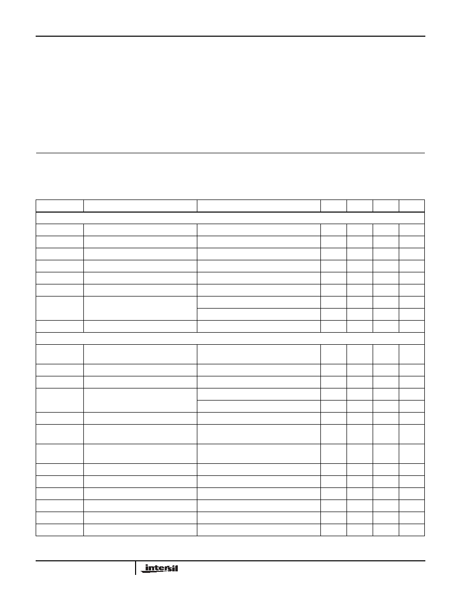
Electrical Specifications
V
IN
= 3V, V
BOOST
= V
SUP
= 12V, V
SRC
= 20V, Over temperature from -40∞C to 85∞C.
Unless Otherwise Specified.
PARAMETER
DESCRIPTION
CONDITIONS
MIN
TYP
MAX
UNIT
SUPPLY
V
IN
Input Supply Range
2.6
5.5
V
V
LOR
Undervoltage Lockout Threshold
V
IN
rising
2.4
2.5
2.6
V
V
LOF
Undervoltage Lockout Threshold
V
IN
falling
2.2
2.3
2.4
V
I
S
Quiescent Current
LX not switching
2.5
mA
I
SS
Quiescent Current - Switching
LX switching
5
10
mA
T
FD
Fault Delay Time
C
DEL
= 220nF
52
ms
V
REF
Reference Voltage
T
A
= 25∞C
1.19
1.215
1.235
V
1.187
1.215
1.238
V
SHUTDN
Thermal Shutdown Temperature
140
∞C
MAIN BOOST REGULATOR
V
BOOST
Output Voltage Range
(Note 1)
V
IN
+
15%
18
V
F
OSC
Oscillator Frequency
1050
1200
1350
kHz
D
CM
Maximum Duty Cycle
82
85
%
V
FBB
Boost Feedback Voltage
T
A
= 25∞C
1.192
1.205
1.218
V
1.188
1.205
1.222
V
V
FTB
FB Fault Trip Level
Falling edge
0.85
0.925
1.020
V
V
BOOST
/
I
BOOST
Load Regulation
50mA < I
LOAD
< 250mA
0.1
%
V
BOOST
/
V
IN
Line Regulation
V
IN
= 2.6V to 5.5V
0.08
%/V
I
FB
Input Bias Current
V
FB
= 1.35V
500
nA
gmV
FB Transconductance
dI = ±2.5µA at COMP, FB = COMP
160
µA/V
R
ON
LX
LX On Resistance
160
m
I
LEAK
LX
LX Leakage Current
V
FB
= 1.35V, V
LX
= 13V
0.02
40
µA
I
LIM
LX
LX Current Limit
Duty cycle = 65% (Note 1)
3.0
A
t
SS
B
Soft-Start Period
C
DEL
= 220nF
2
ms
EL7640, EL7641, EL7642

4
FN7415.1
September 26, 2005
OPERATIONAL AMPLIFIERS
V
SUP
Supply Operating Range
4.5
18
V
I
SUP
Supply Current per Amplifier
600
800
µA
V
OS
Offset Voltage
3
12
mV
I
B
Input Bias Current
-50
+50
nA
CMIR
Common Mode Input Range
0
V
SUP
V
CMRR
Common Mode Rejection Ratio
60
90
dB
A
OL
Open Loop Gain
110
dB
V
OH
Output Voltage High
I
OUT
= 100µA
V
SUP
-15
V
SUP
-2
mV
I
OUT
= 5mA
V
SUP
-250
V
SUP
-150
mV
V
OL
Output Voltage Low
I
OUT
= -100µA
2
30
mV
I
OUT
= -5mA
100
150
mV
I
SC
Short-Circuit Current
100
150
mA
I
CONT
Continuous Output Current
±50
mA
PSRR
Power Supply Rejection Ratio
60
100
dB
BW
-3dB
-3dB Bandwidth
12
MHz
GBWP
Gain Bandwidth Product
8
MHz
SR
Slew Rate
12
V/µs
POSITIVE LDO
V
FBP
Positive Feedback Voltage
I
DRVP
= 100µA, T
A
= 25∞C
1.176
1.2
1.224
V
I
DRVP
= 100µA
1.176
1.2
1.229
V
V
FTP
V
FBP
Fault Trip Level
V
FBP
falling
0.82
0.9
0.98
V
I
BP
Positive LDO Input Bias Current
V
FBP
= 1.4V
-50
50
nA
V
POS
/
I
POS
FBP Load Regulation
V
DRVP
= 25V, I
DRVP
= 0 to 20µA
0.5
%
I
DRVP
Sink Current
V
FBP
= 1.1V, V
DRVP
= 10V
2
4
mA
I
LEAK
P
DRVP Off Leakage Current
V
FBP
= 1.4V, V
DRVP
= 30V
0.1
10
µA
t
SS
P
Soft-Start Period
C
DEL
= 220nF
2
ms
NEGATIVE LDO
V
FBN
FBN Regulation Voltage
I
DRVN
= 0.2mA, T
A
= 25∞C
0.173
0.203
0.233
V
I
DRVN
= 0.2mA
0.171
0.203
0.235
V
V
FTN
V
FBN
Fault Trip Level
V
FBN
rising
380
430
480
mV
I
BN
Negative LDO Input Bias Current
V
FBN
= 250mV
-50
50
nA
FBN Load Regulation
V
DRVN
= -6V, I
DRVN
= 2µA to 20µA
0.5
%
I
DRVN
Source Current
V
FBN
= 500mV, V
DRVN
= -6V
2
4
mA
I
LEAK
N
DRVN Off Leakage Current
V
FBP
= 1.35V, V
DRVP
= 30V
0.1
10
µA
t
SS
N
Soft-start Period
C
DEL
= 220nF
2
ms
Electrical Specifications
V
IN
= 3V, V
BOOST
= V
SUP
= 12V, V
SRC
= 20V, Over temperature from -40∞C to 85∞C.
Unless Otherwise Specified. (Continued)
PARAMETER
DESCRIPTION
CONDITIONS
MIN
TYP
MAX
UNIT
EL7640, EL7641, EL7642

5
FN7415.1
September 26, 2005
V
ON
-SLICE CIRCUIT
V
LO
CTL Input Low Voltage
V
IN
= 2.6V to 5.5V
0.4V
IN
V
V
HI
CTL Input High Voltage
V
IN
= 2.6V to 5.5V
0.6V
IN
V
I
LEAK
CTL
CTL Input Leakage Current
CTL = AGND or IN
-1
1
µA
t
D
rise
CTL to OUT Rising Prop Delay
1k
from DRN to 8V, V
CTL
= 0V to 3V step,
no load on OUT, measured from V
CTL
= 1.5V
to OUT = 20%
100
ns
t
D
fall
CTL to OUT Falling Prop Delay
1k
from DRN to 8V, V
CTL
= 3V to 0V step,
no load on OUT, measured from V
CTL
= 1.5V
to OUT = 80%
100
ns
V
SRC
SRC Input Voltage Range
30
V
ISRC
SRC Input Current
Start-up sequence not completed
150
250
µA
Start-up sequence completed
150
250
µA
R
ON
SRC
SRC On Resistance
Start-up sequence completed
5
10
R
ON
DRN
DRN On Resistance
Start-up sequence completed
30
60
R
ON
COM
COM to GND On Resistance
Start-up sequence not completed
350
1000
1800
SEQUENCING
t
ON
Turn On Delay
C
DLY
= 0.22µF (See Figure 23)
30
ms
t
DEL1
Delay Between V
BOOST
and V
OFF
C
DLY
= 0.22µF (See Figure 23)
10
ms
t
DEL2
Delay Between V
ON
and V
OFF
C
DLY
= 0.22µF (See Figure 23)
17
ms
t
DEL3
Delay From V
ON
to V
ON
-slice Enabled
C
DLY
= 0.22µF (See Figure 23)
10
ms
C
DEL
Delay Capacitor
50
220
nF
NOTE:
1. Guaranteed by design.
Electrical Specifications
V
IN
= 3V, V
BOOST
= V
SUP
= 12V, V
SRC
= 20V, Over temperature from -40∞C to 85∞C.
Unless Otherwise Specified. (Continued)
PARAMETER
DESCRIPTION
CONDITIONS
MIN
TYP
MAX
UNIT
EL7640, EL7641, EL7642