 | –≠–ª–µ–∫—Ç—Ä–æ–Ω–Ω—ã–π –∫–æ–º–ø–æ–Ω–µ–Ω—Ç: EL7761CS | –°–∫–∞—á–∞—Ç—å:  PDF PDF  ZIP ZIP |
1
Æ
FN7299
CAUTION: These devices are sensitive to electrostatic discharge; follow proper IC Handling Procedures.
1-888-INTERSIL or 321-724-7143
|
Intersil (and design) is a registered trademark of Intersil Americas Inc.
Copyright © Intersil Americas Inc. 2003. All Rights Reserved. Elantec is a registered trademark of Elantec Semiconductor, Inc.
All other trademarks mentioned are the property of their respective owners.
EL7761
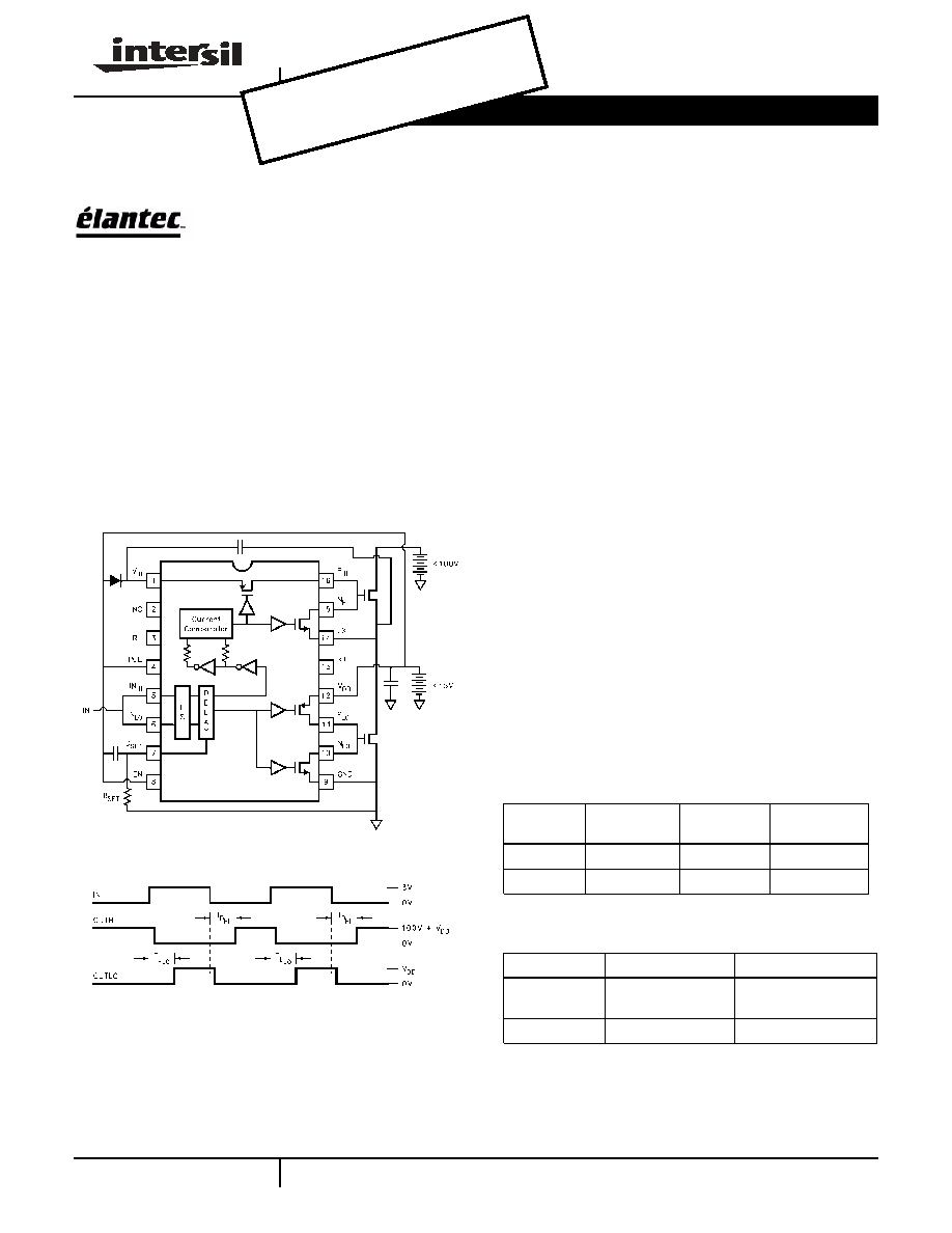
100V Half Bridge Driver
The EL7761 provides a low cost
solution to many half bridge
applications. The EL7761 is DC
coupled so that there are no start up problems associated
with AC coupled schemes. A single resistor from D
SET
to
GND provides "dead time" programmability. Shorting D
SET
to V
DD
gives the shortest delay (~100ns).
The POL pin controls the polarity of the low side driver. The
polarity of the upper driver is always inverting. The EN pin,
when low, forces the high and low side outputs into their low
state.
Pinout
Features
∑ 100V High Side Voltage
∑ Programmable Delay
∑ Direct Coupled
∑ No Start Up Ambiguity
∑ Rail to Rail Output
∑ 1MHz Operation
∑ Shutdown Function
∑ 1.0 Amp Peak Current
∑ Improved Response Times
∑ Matched Rise and Fall Times
∑ Low Supply Current
∑ Low Output Impedance
∑ Low Input Capacitance
Applications
∑ Uninterruptible Power Supplies
∑ Distributed Power Systems
∑ IGBT Drive
∑ DC-DC Converters
∑ Motor Control
∑ Power MOSFET Drive
∑ Switch Mode Power Supplies
NOTE: Contact factory
EL7761 WAVEFORM EXAMPLE
T
DLO
= T
DHI
POL = V
DD
EL7761
(16-PIN PDIP, SOIC)
TOP VIEW
Ordering Information
PART
NUMBER
TEMP. RANGE
PACKAGE
PKG. NO.
EL7761CN
-40∞C to +85∞C
16-Pin PDIP
MDP0031
EL7761CS
-40∞C to +85∞C
16-Pin SOIC
MDP0027(Note)
POL
POLARITY
Low Side
GND
V
DD
Inverting
Non-Inverting
Hi Side
X
Inverting
Data Sheet
January 1996, Rev C
OBS
OLE
TE P
ROD
UCT
NO
REC
OMM
END
ED R
EPL
ACE
MEN
T
con
tact
our
Tech
nica
l Su
ppo
rt Ce
nter
at
1-88
8-IN
TER
SIL
or w
ww.
inter
sil.c
om/
tsc
2
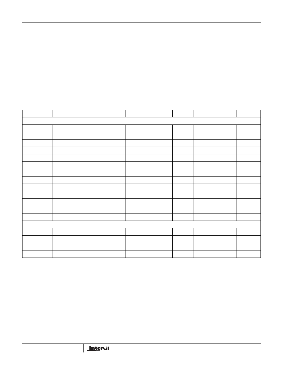
Absolute Maximum Ratings
(T
A
= 25∞C)
Supply (V
HI
to GND) . . . . . . . . . . . . . . . . . . . . . . . . . . . . . . . . .100V
Supply (V
DD
to GND) . . . . . . . . . . . . . . . . . . . . . . . . . . . . . . . 16.5V
Input Pins . . . . . . . . . . . . . . . . . . . . . . . . . . . . . . . -0.3V below GND,
. . . . . . . . . . . . . . . . . . . . . . . . . . . . . . . . . . . . . . . .+0.3V above V
DD
Peak Current per Output . . . . . . . . . . . . . . . . . . . . . . . . . . . . . . . .2A
Storage Temperature Range . . . . . . . . . . . . . . . . . . -65∞C to +150∞C
Ambient Operating Temperature . . . . . . . . . . . . . . . . -40∞C to +85∞C
Operating Junction Temperature . . . . . . . . . . . . . . . . . . . . . . . 125∞C
Power Dissipation
SOIC . . . . . . . . . . . . . . . . . . . . . . . . . . . . . . . . . . . . . . . . . . 1100mW
PDIP . . . . . . . . . . . . . . . . . . . . . . . . . . . . . . . . . . . . . . . . . . 1800mW
CAUTION: Stresses above those listed in "Absolute Maximum Ratings" may cause permanent damage to the device. This is a stress only rating and operation of the
device at these or any other conditions above those indicated in the operational sections of this specification is not implied.
IMPORTANT NOTE: All parameters having Min/Max specifications are guaranteed. Typical values are for information purposes only. Unless otherwise noted, all tests
are at the specified temperature and are pulsed tests, therefore: T
J
= T
C
= T
A
DC Electrical Specifications
T
A
= 25∞C, V
DD
= 15V, C
LOAD
= 1000pF, unless otherwise specified
PARAMETER
DESCRIPTION
TEST CONDITIONS
MIN
TYP
MAX
UNITS
INPUT/OUTPUT
V
IH
Logic "1" Input Voltage
3.0
2.4
V
I
IH
Logic "1" Input Current
0.1
10.0
µA
V
IL
Logic "0" Input Voltage
1.8
0.8
V
I
IL
Logic "0" Input Current
0.1
10.0
µA
V
HVS
Input Hysteresis
0.5
V
V
ENH
Enable Threshold
Positive Edge
2.8
1.6
V
V
ENL
Disable Threshold
Negative Edge
0.9
0.6
V
V
EN HYS
Enable Hysteresis
0.7
V
I
DS OFF
Output Leakage
GND
V
OUT
V
DD
-10.0
0.2
10.0
µA
R
OH
Pull-up Resistance
I
OUT
= -100mA
5.0
10.0
R
OL
Pull-down Resistance
I
OUT
= +100mA
5.0
10.0
I
PK
Peak Output Current
1.0
A
I
DC
Continuous Output Current Source/Sink
50.0
mA
POWER SUPPLY
I
DD
Supply Current into V
DD
R
SET
= 5.1k
6.0
10.0
mA
I
HI
Supply Current into V
HI
2.0
4.0
mA
I
DD OFF
Supply Current into V
DD
V
EN
= 0.6V
750.0
uA
V
DD
Operating Voltage
4.5
15.0
V
EL7761

3
AC Electrical Specifications
T
A
= 25∞C, V
DD
= 15V, C
LOAD
= 1000pF, unless otherwise specified
PARAMETER
DESCRIPTION
TEST CONDITIONS
MIN
TYP
MAX
UNITS
SWITCHING CHARACTERISTICS
t
R
Rise Time
C
L
= 500pF
C
L
= 1000pF
15.0
20.0
40.0
ns
t
F
Fall Time
C
L
= 500pF
C
L
= 1000pF
15.0
20.0
40.0
ns
t
D ON HI
High Side Turn On Delay Time
D
SET
= V
DD
R
SET
= 5.1k
R
SET
= 400k
50.0
75.0
750.0
100.0
125.0
1150.0
150.0
200.0
1500.0
ns
t
D ON LO
Low Side Turn On Delay Time
D
SET
= V
DD
R
SET
= 5.1k
R
SET
= 400k
50.0
75.0
750.0
100.0
125.0
1150.0
150.0
200.0
1500.0
ns
t
D OFF HI
High Side Turn Off Delay Time
D
SET
= V
DD
100.0
150.0
ns
t
D OFF LO
Low Side Turn Off Delay Time
D
SET
= V
DD
100.0
150.0
ns
t
D MISMATCH
High to Lo Side Turn On Delay Mismatch
R
SET
= 400k
±10.0
%
Pin Descriptions
PIN #
NAME
FUNCTION
1
V
HI
Positive supply for the high side driver.
2
NC
3
R
-
Internal connection between the low side and high side driver. This pin is normally unconnected.
4
P
OL
Controls the polarity of the low side driver.
5
IN
HI
Logic input for the high side driver.
6
IN
LO
Logic input for the low side driver.
7
D
SET
Connection for the delay adjust resistor.
8
EN
A high voltage on this pin enables the part.
9
GND
Negative supply of the low side driver and control circuitry.
10
N
LO
Low side driver output pull down.
11
P
LO
Low side driver output pull up.
12
V
DD
Positive supply of the low side driver and control circuitry.
13
R
+
Internal connection between the low side and high side driver. This pin is normally unconnected.
14
LX
Negative supply for the high side driver.
15
N
HI
High side driver output pull down.
16
P
HI
High side driver output pull up.
EL7761
4
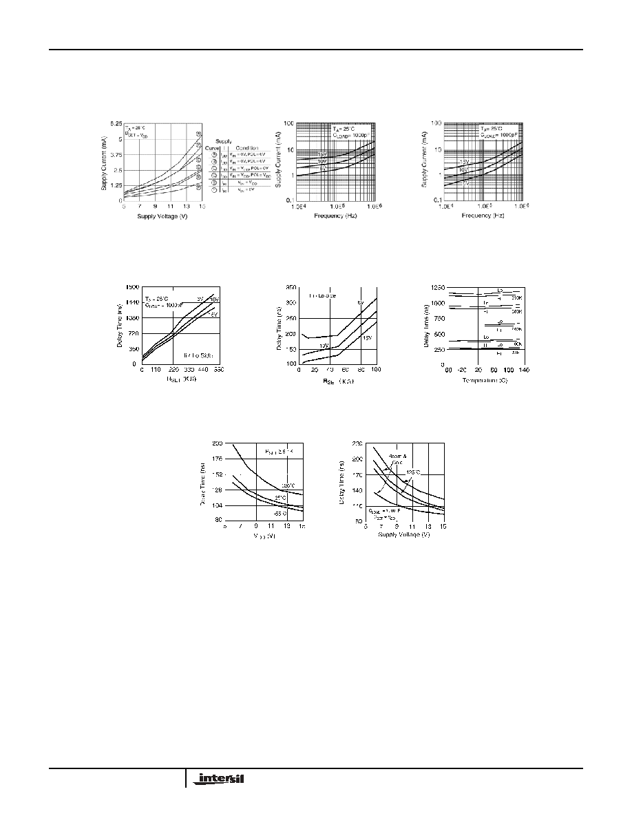
Typical Performance Curves
Quiescent Supply
Current vs. Supply Voltage
Avg. Supply Current
into V
DD
vs.
Voltage and Frequency
Average Supply Current
into V
HI
vs.
Voltage and Frequency
Output Rising Edge
Delay vs. R
SET
and Supply Voltage
Output Rising Edge
Delay vs. R
SET
and
Supply Voltage (Detail)
Output Rising Edge
Delay vs. Temperature
and R
SET
Output Falling Edge Delay
vs. Supply Voltage and
Temperature
Delay Times* vs.
Supply Voltage
and Temperature
*Minimum Rising and Falling Edge Delay Time
EL7761
5
All Intersil U.S. products are manufactured, assembled and tested utilizing ISO9000 quality systems.
Intersil Corporation's quality certifications can be viewed at www.intersil.com/design/quality
Intersil products are sold by description only. Intersil Corporation reserves the right to make changes in circuit design, software and/or specifications at any time without
notice. Accordingly, the reader is cautioned to verify that data sheets are current before placing orders. Information furnished by Intersil is believed to be accurate and
reliable. However, no responsibility is assumed by Intersil or its subsidiaries for its use; nor for any infringements of patents or other rights of third parties which may result
from its use. No license is granted by implication or otherwise under any patent or patent rights of Intersil or its subsidiaries.
For information regarding Intersil Corporation and its products, see www.intersil.com
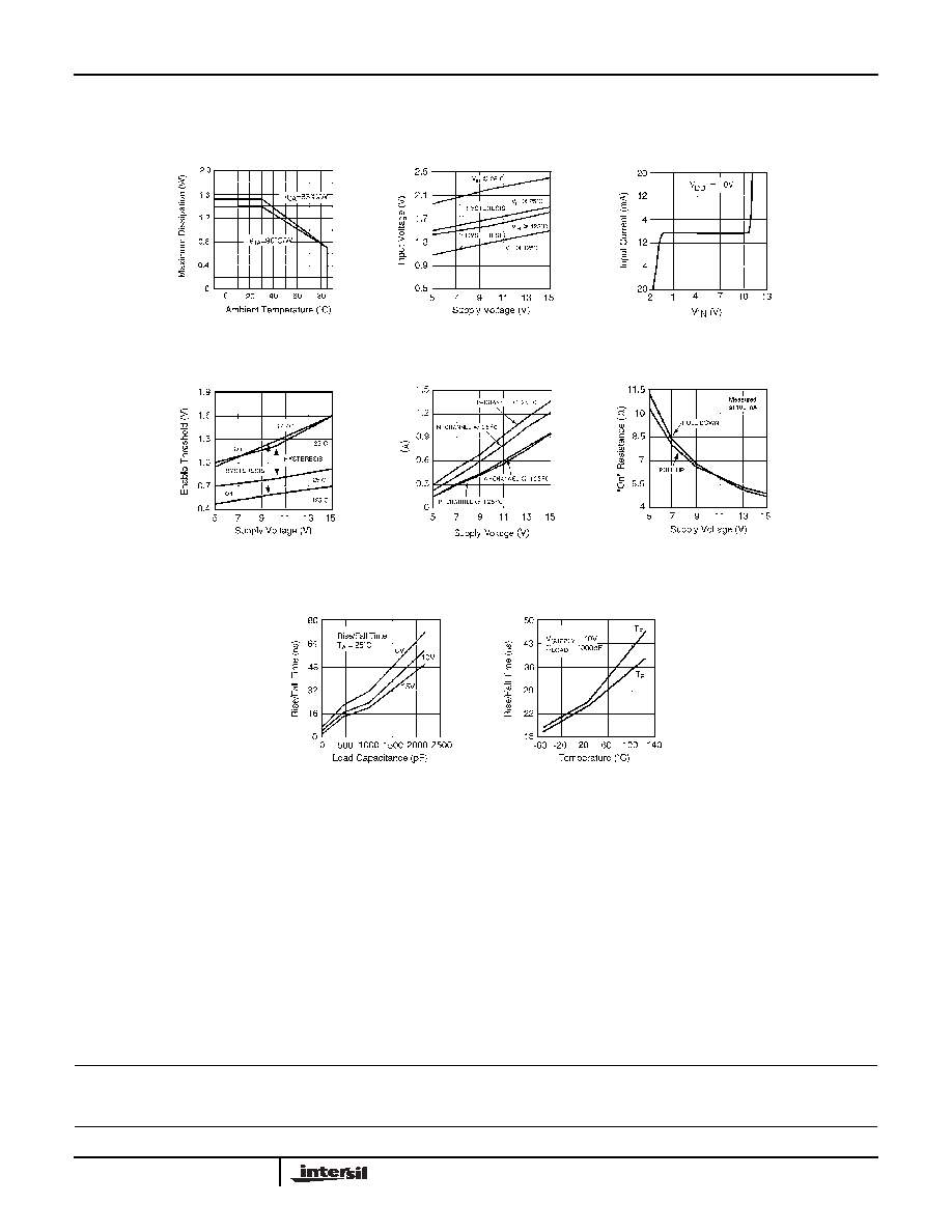
Typical Performance Curves
Max. Power/Derating
Curves
16 Pin Package
Input Threshold vs.
Supply Voltage
Input Current vs.
Input Voltage
Enable Threshold vs.
Supply Voltage
Peak Drive vs.
Supply Voltage
"On" Resistance vs.
Supply Voltage
Rise/Fall Time vs.
Load and Supply
Rise/Fall Time vs.
Temperature
EL7761