 | ÐлекÑÑоннÑй компоненÑ: EL7900 | СкаÑаÑÑ:  PDF PDF  ZIP ZIP |
Äîêóìåíòàöèÿ è îïèñàíèÿ www.docs.chipfind.ru
1
®
FN7377.0
CAUTION: These devices are sensitive to electrostatic discharge; follow proper IC Handling Procedures.
1-888-INTERSIL or 1-888-468-3774
|
Intersil (and design) is a registered trademark of Intersil Americas Inc.
Copyright © Intersil Americas Inc. 2005. All Rights Reserved.
All other trademarks mentioned are the property of their respective owners.
PRELIMINARY
EL7900
Ambient Light Photo Detect IC
The EL7900 is a light-to-current optical sensor combining a
photodiode and a current amplifier on a single monolithic IC.
Output current is directly proportionate to the light intensity
on the photodiode. Its sensitivity is superior to that of a
phototransistor and exhibits little variation. Its spectral
sensitivity matches closely to the luminous efficiency and
linearity.
Housed in an ultra-compact surface mount clear plastic
package, this device is excellent for power saving control
function in cell phones, PDAs, and other handheld
applications.
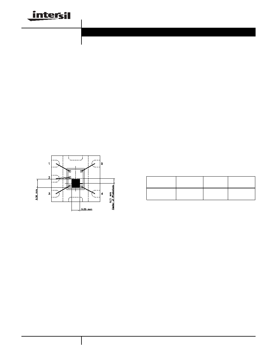
Pinout
EL7900
(5-PIN DFN)
TOP VIEW
Features
· Monolithic IC containing photodiode and amplifier
· Converts light intensity to current
· 2.5V to 5.5V supply range
· Low supply current - 1µA
· Excellent output linearity of luminance
· Ultra-compact and light surface mount package
· Pb-Free plus anneal available (RoHS compliant)
Applications
· Mobile phones
· Notebook PCs
· PDAs
· Video cameras
· Digital cameras
VCC
GND
EN
OUTPUT
NC
Ordering Information
PART NUMBER
PACKAGE
TAPE &
REEL
PKG. DWG. #
EL7900ILCZ
(See Note)
5-Pin ODFN
(Pb-free)
-
MDP0052
NOTE: Intersil Pb-free plus anneal products employ special Pb-free
material sets; molding compounds/die attach materials and 100%
matte tin plate termination finish, which are RoHS compliant and
compatible with both SnPb and Pb-free soldering operations. Intersil
Pb-free products are MSL classified at Pb-free peak reflow
temperatures that meet or exceed the Pb-free requirements of
IPC/JEDEC J STD-020.
Data Sheet
June 20, 2005
2
FN7377.0
June 20, 2005
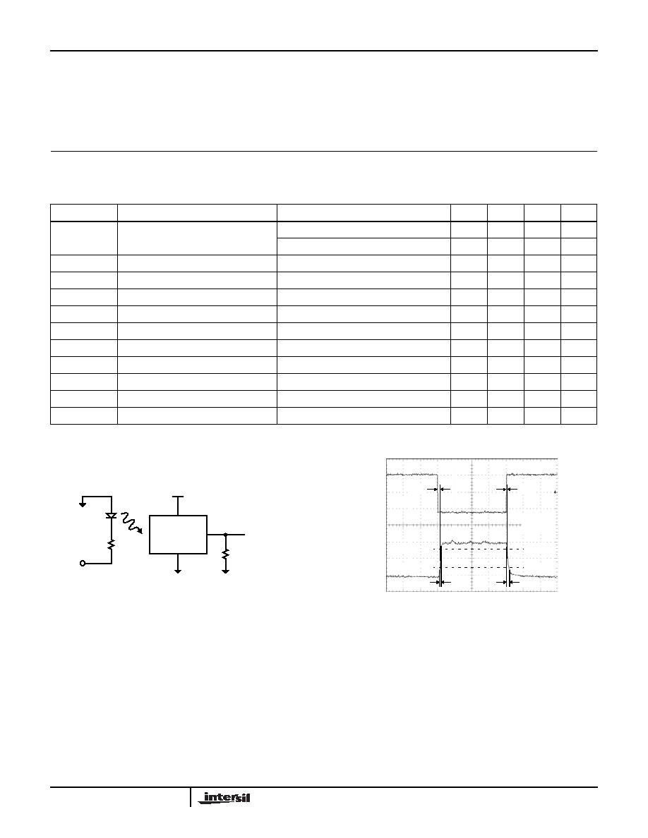
FIGURE 1. RISE/FALL TIME MEASUREMENT
FIGURE 2.
Absolute Maximum Ratings
(T
A
= 25°C)
Supply Voltage between V
SD
and GND . . . . . . . . . . . . . . . . . . . .6V
Maximum Continuous Output Current . . . . . . . . . . . . . . . . . . . . TBD
Operating Temperature . . . . . . . . . . . . . . . . . . . . . . .-40°C to +85°C
Maximum Die Temperature . . . . . . . . . . . . . . . . . . . . . . . . . . +125°C
Storage Temperature . . . . . . . . . . . . . . . . . . . . . . . .-65°C to +150°C
CAUTION: Stresses above those listed in "Absolute Maximum Ratings" may cause permanent damage to the device. This is a stress only rating and operation of the
device at these or any other conditions above those indicated in the operational sections of this specification is not implied.
IMPORTANT NOTE: All parameters having Min/Max specifications are guaranteed. Typical values are for information purposes only. Unless otherwise noted, all tests
are at the specified temperature and are pulsed tests, therefore: T
J
= T
C
= T
A
Electrical Specifications
V
CC
= 3V, T
A
= 25°C, fluorescent light, unless otherwise specified.
PARAMETER
DESCRIPTION
CONDITION
MIN
TYP
MAX
UNIT
I
CC
Supply Current
R
L
= 1k
, EV = 100lx
62
µA
EV = 0lx
1
µA
I
L1
Light Current
EV = 100lx
39
60.5
82
µA
I
L2
Light Current
EV = 10lx
6.2
µA
I
LEAK
Dark Current
EV = 0lx
0.15
µA
V
O-MAX
Maximum Output Compliance Voltage
at 95% of nominal output current, EV = 100lx
2.7
V
T
R
Rise Time (See Note)
R
L
= 5k
, EV = 300lx
105
125
µs
T
F
Fall Time (See Note)
R
L
= 5k
, EV = 300lx
170
225
µs
T
D
Delay Time for Rising Edge (See Note)
R
L
= 5k
, EV = 300lx
165
200
µs
T
S
Delay Time for Falling Edge (See Note)
R
L
= 5k
, EV = 300lx
65
85
µs
V
LO
Maximum Voltage at EN Pin to Enable
0.6
V
V
HI
Minimum Voltage at EN Pin to Disable
1.8
V
NOTE: Switching time measurement is based on Figures 1 and 2.
EL7900
PULSE
DRIVE
V
CC
R
L
V
OUT
CH1
CH2
PULSE DRIVE
V
OUT
T
D
T
R
80%
20%
T
S
T
F
1mS
1V
0.5V
V
S
=3V
T
A
=27°C
EL7900
3
FN7377.0
June 20, 2005
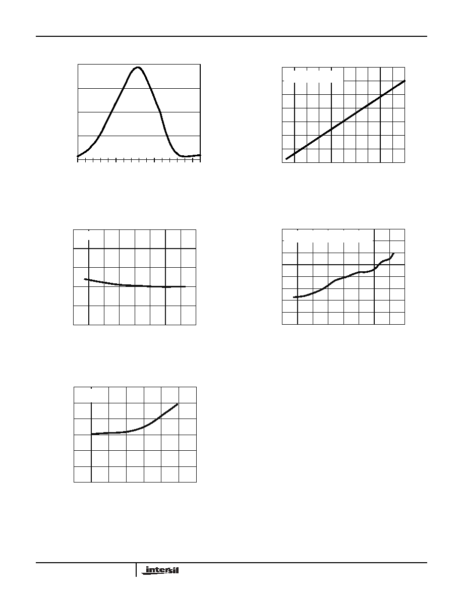
Typical Performance Curves
FIGURE 3. RELATIVE SENSITIVITY
FIGURE 4. SENSITIVITY
FIGURE 5. DARK CURRENT vs TEMPERATURE
FIGURE 6. GAIN vs TEMPERATURE
FIGURE 7. OUTPUT COMPLIANCE VOLTAGE vs CURRENT
SPECTRAL WAVELENGTH (nm)
RE
LA
TIV
E
S
E
NS
IT
IV
ITY
(
%
)
42
8
44
4
46
0
47
6
49
2
50
8
52
4
54
0
55
6
57
2
58
8
60
4
62
0
63
6
65
2
66
8
100
75
50
25
0
ILLUMINATION (L
X
)
OUTPUT CURR
E
N
T
(µA)
700
600
400
200
0
500
300
100
0
200
400
600
800
1000
V
CC
= 3V
FLUORESCENT LIGHT
TEMPERATURE (°C)
OUTPUT
CURRENT - N
O
LIGHT (µA)
0.2
0.18
0.14
0.1
0.16
0.12
-60
-40
0
40
80
100
-20
20
60
V
DD
=3V
TEMPERATURE (°C)
GAIN/GA
I
N (25°
C)
1.2
1.15
0.95
0.8
1.05
0.85
-60
-40
0
40
80
100
-20
20
60
1.1
0.9
1
V
DD
=3V
FLUORESCENT LIGHT OF 50 LUX
OUTPUT CURRENT (µA)
OUTPUT COMPLIANC
E
V
O
L
T
AGE
(V
DD
-V
OU
T
) (V
)
0.6
0.5
0.2
0
0.3
0.1
-200
0
400
800
1000 1200
200
600
V
DD
=3V
T
A
=27°C
0.4
EL7900
4
FN7377.0
June 20, 2005
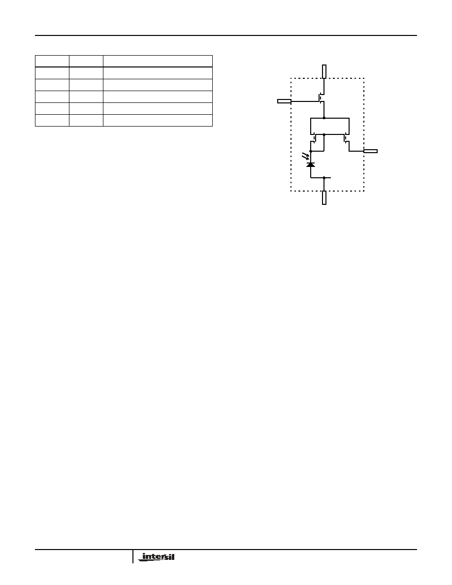
Block Diagram
Pin Descriptions
PIN
NAME
DESCRIPTION
1
VCC
Supply, 2.5V to 5.5V
2
GND
Ground
3
EN
Enable
4
NC
No connect
5
Output
Current output pin
ENABLE
OUTPUT
GND
VCC
1
2
5
3
EL7900
5
All Intersil U.S. products are manufactured, assembled and tested utilizing ISO9000 quality systems.
Intersil Corporation's quality certifications can be viewed at www.intersil.com/design/quality
Intersil products are sold by description only. Intersil Corporation reserves the right to make changes in circuit design, software and/or specifications at any time without
notice. Accordingly, the reader is cautioned to verify that data sheets are current before placing orders. Information furnished by Intersil is believed to be accurate and
reliable. However, no responsibility is assumed by Intersil or its subsidiaries for its use; nor for any infringements of patents or other rights of third parties which may result
from its use. No license is granted by implication or otherwise under any patent or patent rights of Intersil or its subsidiaries.
For information regarding Intersil Corporation and its products, see www.intersil.com
FN7377.0
June 20, 2005
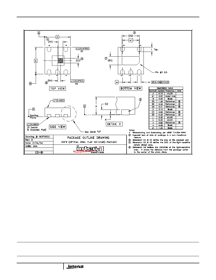
Package Outline Drawing
NOTE: The package drawing shown here may not be the latest version. To check the latest revision, please refer to the Intersil website at
http://www.intersil.com/design/packages/index.asp
EL7900