Äîêóìåíòàöèÿ è îïèñàíèÿ www.docs.chipfind.ru
1
®
FN7103.7
EL8100, EL8101
200MHz Rail-to-Rail Amplifiers
The EL8100 and EL8101 represent single rail-to-rail
amplifiers with a -3dB bandwidth of 200MHz and slew rate of
200V/µs. Running off a very low 2mA supply current, the
EL8100 and EL8101 also feature inputs that go to 0.15V
below the V
S
- rail.
The EL8100 includes a fast-acting disable/power-down
circuit. With a 25ns disable and a 200ns enable, the EL8100
is ideal for multiplexing applications.
The EL8100 and EL8101 are designed for a number of
general purpose video, communication, instrumentation, and
industrial applications. The EL8100 is available in 8-pin SO
and 6-pin SOT-23 packages and the EL8101 is available in a
5-pin SOT-23 package. All are specified for operation over
the -40°C to +85°C temperature range.
Features
· 200MHz -3dB bandwidth
· 200V/µs slew rate
· Low supply current = 2mA
· Supplies from 3V to 5.0V
· Rail-to-rail output
· Input to 0.15V below V
S
-
· Fast 25ns disable (EL8100 only)
· Low cost
· Pb-Free available (RoHS compliant)
Applications
· Video amplifiers
· Portable/hand-held products
· Communications devices
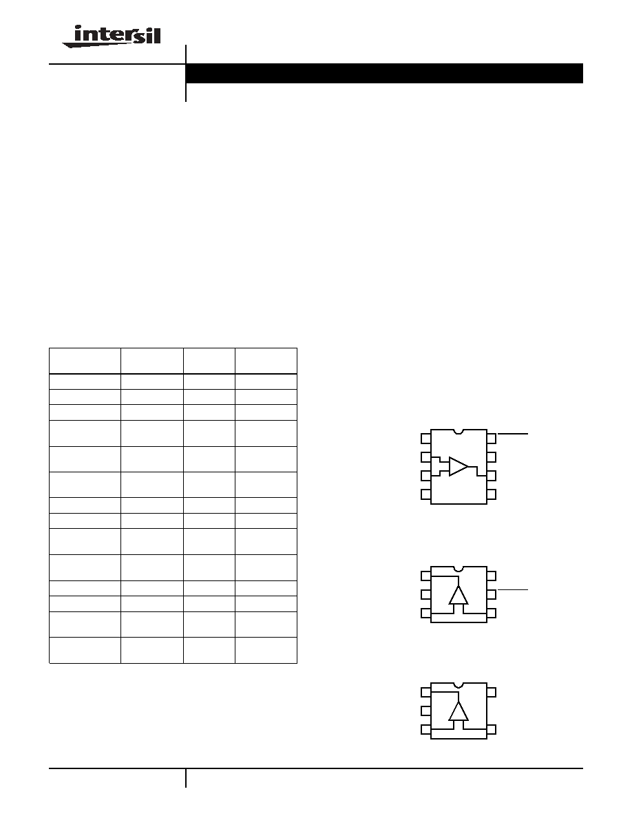
Pinouts
EL8100
(8-PIN SO)
TOP VIEW
EL8100
(6-PIN SOT-23)
TOP VIEW
EL8101
(5-PIN SOT-23)
TOP VIEW
Ordering Information
PART
NUMBER
PACKAGE
TAPE &
REEL
PKG. DWG. #
EL8100IS
8-Pin SO
-
MDP0027
EL8100IS-T7
8-Pin SO
7"
MDP0027
EL8100IS-T13
8-Pin SO
13"
MDP0027
EL8100ISZ
(See Note)
8-Pin SO
(Pb-Free)
-
MDP0027
EL8100ISZ-T7
(See Note)
8-Pin SO
(Pb-Free)
7"
MDP0027
EL8100ISZ-T13
(See Note)
8-Pin SO
(Pb-Free)
13"
MDP0027
EL8100IW-T7
6-Pin SOT-23
7" (3K pcs)
MDP0038
EL8100IW-T7A
6-Pin SOT-23
7" (250 pcs)
MDP0038
EL8100IWZ-T7
(See Note)
6-Pin SOT-23
(Pb-free)
7" (3K pcs)
MDP0038
EL8100IWZ-T7A
(See Note)
6-Pin SOT-23
(Pb-free)
7" (250 pcs)
MDP0038
EL8101IW-T7
5-Pin SOT-23
7" (3K pcs)
MDP0038
EL8101IW-T7A
5-Pin SOT-23
7" (250 pcs)
MDP0038
EL8101IWZ-T7
(See Note)
5-Pin SOT-23
(Pb-Free)
7" (3K pcs)
MDP0038
EL8101IWZ-T7A
(See Note)
5-Pin SOT-23
(Pb-Free)
7" (250 pcs)
MDP0038
NOTE: Intersil Pb-free products employ special Pb-free material sets;
molding compounds/die attach materials and 100% matte tin plate
termination finish, which are RoHS compliant and compatible with
both SnPb and Pb-free soldering operations. Intersil Pb-free products
are MSL classified at Pb-free peak reflow temperatures that meet or
exceed the Pb-free requirements of IPC/JEDEC J STD-020C.
1
2
3
4
8
7
6
5
-
+
NC
IN-
IN+
VS-
ENABLE
VS+
OUT
NC
1
2
3
6
4
5
-
+
OUT
VS-
IN+
VS+
ENABLE
IN-
1
2
3
5
4
-
+
OUT
VS-
IN+
VS+
IN-
Data Sheet
April 26, 2005
CAUTION: These devices are sensitive to electrostatic discharge; follow proper IC Handling Procedures.
1-888-INTERSIL or 1-888-352-6832
|
Intersil (and design) is a registered trademark of Intersil Americas Inc.
Copyright Intersil Americas Inc. 2003-2005. All Rights Reserved
All other trademarks mentioned are the property of their respective owners.
2
FN7103.7
April 26, 2005
IMPORTANT NOTE: All parameters having Min/Max specifications are guaranteed. Typ values are for information purposes only. Unless otherwise noted, all tests are
at the specified temperature and are pulsed tests, therefore: T
J
= T
C
= T
A
Absolute Maximum Ratings
(T
A
= 25°C)
Supply Voltage from V
S
+ to V
S
- . . . . . . . . . . . . . . . . . . . . . . . . 5.5V
Input Voltage . . . . . . . . . . . . . . . . . . . . . . . . V
S
+ +0.3V to V
S
- -0.3V
Differential Input Voltage . . . . . . . . . . . . . . . . . . . . . . . . . . . . . . . .2V
Continuous Output Current . . . . . . . . . . . . . . . . . . . . . . . . . . . 40mA
Power Dissipation . . . . . . . . . . . . . . . . . . . . . . . . . . . . . See Curves
Storage Temperature . . . . . . . . . . . . . . . . . . . . . . . .-65°C to +125°C
Ambient Operating Temperature . . . . . . . . . . . . . . . .-40°C to +85°C
Operating Junction Temperature . . . . . . . . . . . . . . . . . . . . . . +125°C
CAUTION: Stresses above those listed in "Absolute Maximum Ratings" may cause permanent damage to the device. This is a stress only rating and operation of the
device at these or any other conditions above those indicated in the operational sections of this specification is not implied.
Electrical Specifications
V
S
+
= 5V, V
S
-
= GND, T
A
= 25°C, V
CM
= 2.5V, R
L
to 2.5V, A
V
= 1, Unless Otherwise Specified
PARAMETER
DESCRIPTION
CONDITIONS
MIN
TYP
MAX
UNIT
INPUT CHARACTERISTICS
V
OS
Offset Voltage
-6
-0.8
+6
mV
TCV
OS
Offset Voltage Temperature Coefficient Measured from T
MIN
to T
MAX
3
µV/°C
IB
Input Bias Current
V
IN
= 0V
-2.1
-1.5
µA
I
OS
Input Offset Current
V
IN
= 0V
0.2
0.55
µA
TCI
OS
Input Bias Current Temperature
Coefficient
Measured from T
MIN
to T
MAX
2
nA/°C
CMRR
Common Mode Rejection Ratio
V
CM
= -0.15V to +3.5V
70
90
dB
CMIR
Common Mode Input Range
V
S
- -0.15
V
S
+ -1.5
V
R
IN
Input Resistance
Common Mode
16
M
C
IN
Input Capacitance
0.5
pF
A
VOL
Open Loop Gain
V
OUT
= +1.5V to +3.5V, R
L
= 1k
to GND
75
90
dB
V
OUT
= +1.5V to +3.5V, R
L
= 150
to GND
80
dB
OUTPUT CHARACTERISTICS
R
OUT
Output Resistance
A
V
= +1
30
m
V
OP
Positive Output Voltage Swing
R
L
= 1k
4.85
4.9
V
R
L
= 150
4.6
4.7
V
V
ON
Negative Output Voltage Swing
R
L
= 150
100
150
mV
R
L
= 1k
35
50
mV
I
OUT
Linear Output Current
65
mA
I
SC
(source)
Short Circuit Current
R
L
= 10
60
70
mA
I
SC
(sink)
Short Circuit Current
R
L
= 10
120
140
mA
POWER SUPPLY
PSRR
Power Supply Rejection Ratio
V
S
+ = 4.5V to 5.5V
75
100
dB
I
S-ON
Supply Current - Enabled
2
2.4
mA
I
S-OFF
Supply Current - Disabled
30
µA
ENABLE (EL8100 ONLY)
t
EN
Enable Time
200
ns
t
DS
Disable Time
25
ns
V
IH-ENB
ENABLE Pin Voltage for Power-up
0.8
V
V
IL-ENB
ENABLE Pin Voltage for Shut-down
2
V
EL8100, EL8101
3
FN7103.7
April 26, 2005
I
IH-ENB
ENABLE Pin Input Current High
8.6
µA
I
IL-ENB
ENABLE Pin Input for Current Low
0.01
µA
AC PERFORMANCE
BW
-3dB Bandwidth
A
V
= +1, R
F
= 0
, C
L
= 5pF
200
MHz
A
V
= -1, R
F
= 1k
, C
L
= 5pF
90
MHz
A
V
= +2, R
F
= 1k
, C
L
= 5pF
90
MHz
A
V
= +10, R
F
= 1k
, C
L
= 5pF
10
MHz
BW
±0.1dB Bandwidth
A
V
= +1, R
F
= 0
, C
L
= 5pF
20
MHz
Peak
Peaking
A
V
= +1, R
F
= 1k
, C
L
= 5pF
1
dB
GBWP
Gain Bandwidth Product
100
MHz
PM
Phase Margin
R
L
= 1k
, C
L
= 5pF
55
°
SR
Slew Rate
A
V
= 2, R
L
= 100
, V
OUT
= 0.5V to 4.5V
160
200
V/µs
t
R
Rise Time
2.5V
STEP
, 20% - 80%
8
ns
t
F
Fall Time
2.5V
STEP
, 20% - 80%
7
ns
OS
Overshoot
200mV step
10
%
t
PD
Propagation Delay
200mV step
2
ns
t
S
0.1% Settling Time
200mV step
20
ns
dG
Differential Gain
A
V
= +2, R
F
= 1k
, R
L
= 150
0.035
%
dP
Differential Phase
A
V
= +2, R
F
= 1k
, R
L
= 150
0.05
°
e
N
Input Noise Voltage
f = 10kHz
10
nV/
Hz
i
N
+
Positive Input Noise Current
f = 10kHz
1
pA/
Hz
i
N
-
Negative Input Noise Current
f = 10kHz
0.8
pA/
Hz
Electrical Specifications
V
S
+
= 5V, V
S
-
= GND, T
A
= 25°C, V
CM
= 2.5V, R
L
to 2.5V, A
V
= 1, Unless Otherwise Specified (Continued)
PARAMETER
DESCRIPTION
CONDITIONS
MIN
TYP
MAX
UNIT
Pin Descriptions
PIN
NAME
FUNCTION
EL8100IS
EL8100IW
EL8101IW
1
NC
Not connected
2
4
4
IN-
Inverting input
3
3
3
IN+
non-inverting input
4
2
2
VS-
Negative power supply
5
NC
Not connected
6
1
1
OUT
Amplifier output
7
6
5
VS+
Positive power supply
8
5
ENABLE
Enable and disable input
EL8100, EL8101
4
FN7103.7
April 26, 2005
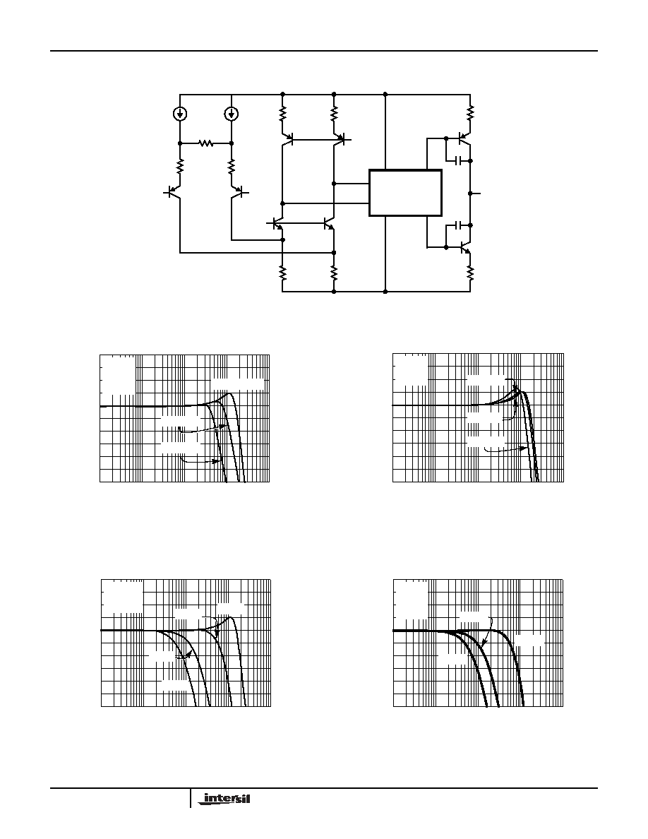
Simplified Schematic Diagram
IN+
IN-
I
1
I
2
R
6
R
3
R
1
R
2
Q
1
Q
2
R
7
V
BIAS1
Q
5
Q
6
R
8
Q
7
Q
8
R
9
Q
3
Q
4
R
4
R
5
V
S-
OUT
V
BIAS2
V
S+
DIFFERENTIAL TO
DRIVE
GENERATOR
SINGLE ENDED
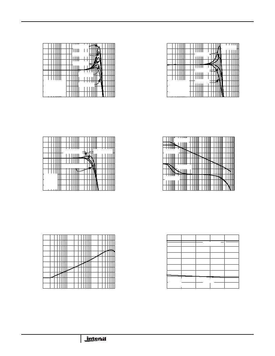
Typical Performance Curves
FIGURE 1. FREQUENCY RESPONSE FOR VARIOUS OUTPUT
VOLTAGE LEVELS
FIGURE 2. Small Signal Frequency Response for Various
R
LOAD
FIGURE 3. Small Signal Frequency Response for Various
Non-Inverting Gains
FIGURE 4. Small Signal Frequency Response for Various
Inverting Gains
4
2
0
-2
-4
-6
100K
1M
10M
100M
1G
FREQUENCY (Hz)
GAI
N
(d
B)
V
S
=5V
A
V
=1
R
L
=1k
C
L
=5pF
V
OP-P
=200mV
V
OP-P
=1V
V
OP-P
=2V
4
2
0
-2
-4
-6
100K
1M
10M
100M
1G
FREQUENCY (Hz)
GAI
N
(d
B)
V
S
=5V
A
V
=1
C
L
=5pF
R
L
=330
R
L
=1k
R
L
=100
4
2
0
-2
-4
-6
100K
1M
10M
100M
1G
FREQUENCY (Hz)
NORMALIZ
E
D
GA
IN
(dB)
V
S
=5V
R
L
=1k
C
L
=5pF
A
V
=1
A
V
=10
A
V
=5
A
V
=2
4
2
0
-2
-4
-6
100K
1M
10M
100M
1G
FREQUENCY (Hz)
NORMA
L
IZED GAIN (dB)
V
S
=5V
R
L
=1k
C
L
=5pF
R
F
=1k
A
V
=-10
A
V
=-2
A
V
=-5
EL8100, EL8101
5
FN7103.7
April 26, 2005
FIGURE 5. Small Signal Frequency Response for Various C
L
FIGURE 6. Small Signal Frequency Response for Various C
L
FIGURE 7. Small Signal Frequency Response for Various R
F
and R
G
FIGURE 8. Open Loop Gain and Phase vs Frequency
FIGURE 9. Common-Mode Rejection Ratio vs Frequency
FIGURE 10. Small Signal Bandwidth vs Supply Voltage
Typical Performance Curves
(Continued)
5
3
1
-1
-3
-5
100K
1M
10M
100M
1G
FREQUENCY (Hz)
G
A
IN
(
d
B)
V
S
=5V
A
V
=1
R
L
=1k
V
OP-P
=200mV
C
L
=15pF
C
L
=1.5pF
C
L
=11.5pF
C
L
=8.3pF
C
L
=5pF
10
8
6
4
2
0
100K
1M
10M
100M
1G
FREQUENCY (Hz)
G
A
IN
(
d
B)
C
L
=15pF
C
L
=5pF
C
L
=56pF
C
L
=35pF
V
S
=5V
A
V
=2
R
L
=1k
R
F
=R
G
=1k
10
8
6
4
2
0
100K
1M
10M
100M
1G
FREQUENCY (Hz)
GAI
N
(
d
B)
V
S
=5V
A
V
=2
R
L
=1k
C
L
=5pF
R
F
=R
G
=2k
R
F
=R
G
=500
R
F
=R
G
=1k
110
70
30
-10
-50
-90
1K
10K
1M
100M
1G
FREQUENCY (Hz)
GAI
N
(
d
B)
R
L
=1k
PHAS
E (
°
)
-45
405
315
225
135
45
100K
10M
R
L
=150
R
L
=150
R
L
=1k
-10
-30
-50
-70
-90
-110
100K
1M
10M
100M
FREQUENCY (Hz)
CMRR (
d
B)
230
170
130
210
70
50
3
3.5
4.5
5
5.5
V
S
(V)
BANDWIDT
H
(MHz)
R
L
=1k
C
L
=5pF
A
V
=1
A
V
=2
190
110
90
150
4
EL8100, EL8101