 | ÐлекÑÑоннÑй компоненÑ: EL8108 | СкаÑаÑÑ:  PDF PDF  ZIP ZIP |
Äîêóìåíòàöèÿ è îïèñàíèÿ www.docs.chipfind.ru
1
®
FN7417
CAUTION: These devices are sensitive to electrostatic discharge; follow proper IC Handling Procedures.
1-888-INTERSIL or 321-724-7143
|
Intersil (and design) is a registered trademark of Intersil Americas Inc.
Copyright © Intersil Americas Inc. 2004. All Rights Reserved. Elantec is a registered trademark of Elantec Semiconductor, Inc.
All other trademarks mentioned are the property of their respective owners.
PRELIMINARY
EL8108
Video Distribution Amplifier
The EL8108 is a dual current feedback
operational amplifier designed for
video distribution solutions. This
device features a high drive capability of 450mA while
consuming only 5mA of supply current per amplifier and
operating from a single 5V to 12V supply.
The EL8108 is available in the industry standard 8-pin SO as
well as the thermally-enhanced 16-pin QFN package. Both
are specified for operation over the full -40°C to +85°C
temperature range. The EL8108 has control pins C0 and C1
for controlling the bias and enable/disable of the outputs.
The EL8108 is ideal for driving multiple video loads while
maintaining linearity.
Features
· Drives up to 450mA from a +12V supply
· 20V
P-P
differential output drive into 100
· -85dBc typical driver output distortion at full output at
150kHz
· -70dBc typical driver output distortion at 3.75MHz
· Low quiescent current of 5mA per amplifier
· 300MHz bandwidth
Applications
· Video distribution amplifiers
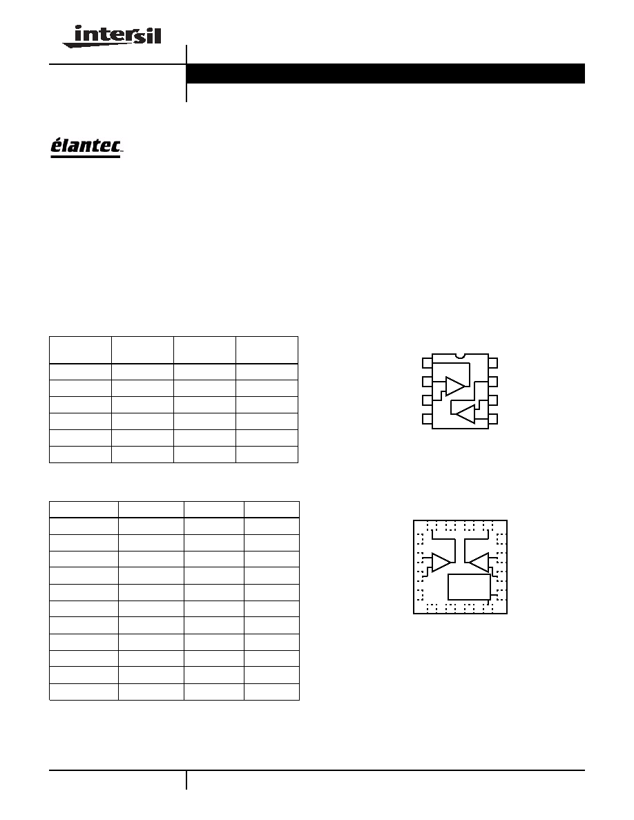
Pinouts
EL8108
(8-PIN SO)
TOP VIEW
EL8108
(16-PIN QFN)
TOP VIEW
Ordering Information
PART
NUMBER
PACKAGE
TAPE & REEL
PKG. DWG. #
EL8108IS
8-Pin SO
-
MDP0027
EL8108IS-T7
8-Pin SO
7"
MDP0027
EL8108IS-T13
8-Pin SO
13"
MDP0027
EL8108IL
16-Pin QFN
-
MDP0046
EL8108IL-T7
16-Pin QFN
7"
MDP0046
EL8108IL-T13
16-Pin QFN
13"
MDP0046
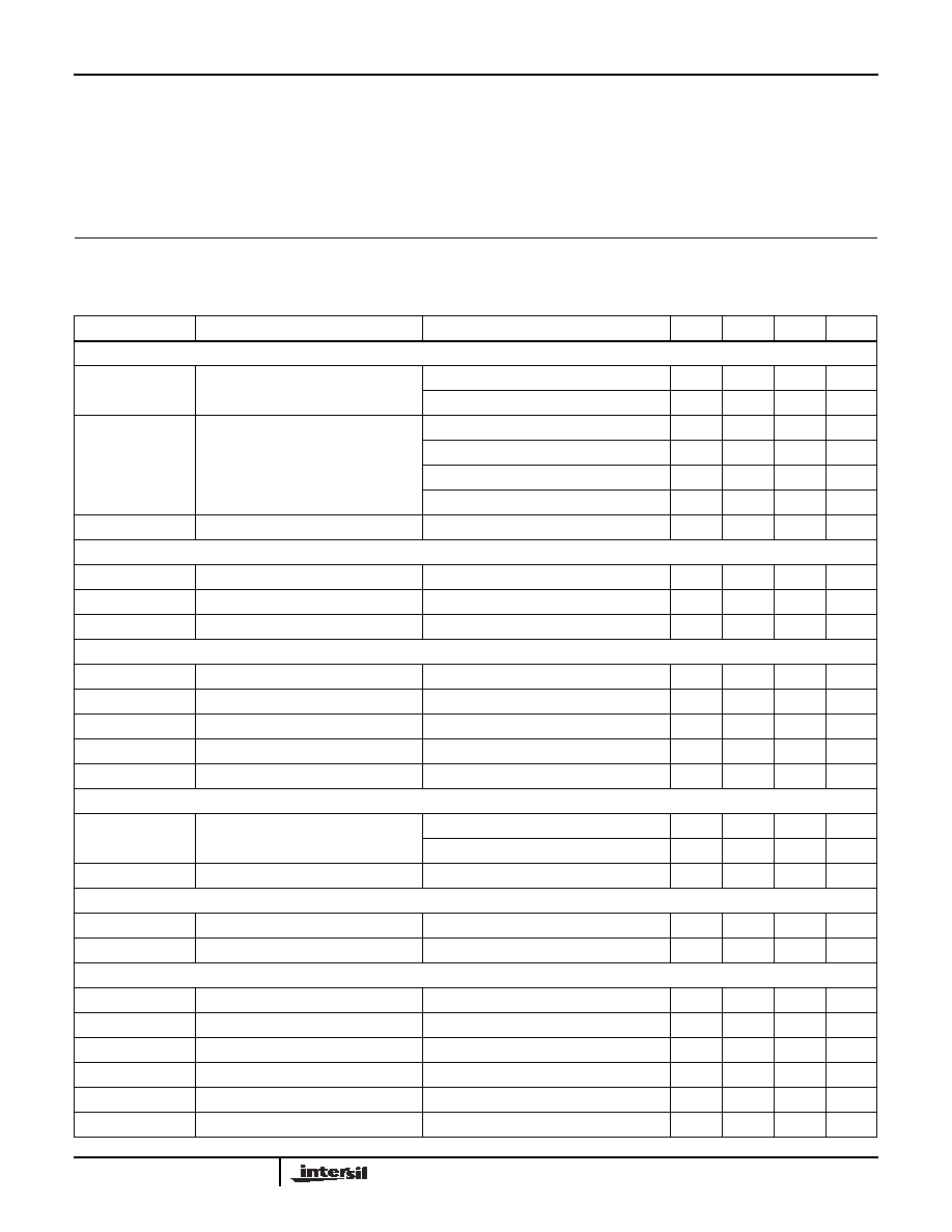
TABLE 1.
150
150
DIFF GAIN
DIFF PHASE
1
0
0.03
0.01
1
1
0.03
0.01
2
1
0.05
0.02
2
2
0.06
0.03
3
2
0.08
0.03
3
3
0.11
0.03
2
0
0.04
0.01
3
0
0.05
0.02
4
0
0.07
0.02
5
0
0.08
0.03
6
0
0.10
0.03
1
2
3
4
8
7
6
5
-
+
INB-
OUTB
INA-
INA+
GND
INB+
VS
OUTA
-
+
1
2
3
4
12
11
10
9
5
6
7
8
16
15
14
13
NC
INA-
INA+
GND
NC
NC
VS
-
C0
OUT
A
NC
VS+
OUT
B
NC
INB-
INB+
C1
-
+
-
+
AMP A
AMP B
POWER
CONTROL
LOGIC
Data Sheet
June 7, 2004
2
Absolute Maximum Ratings
(T
A
= 25°C)
V
S
+ Voltage to Ground . . . . . . . . . . . . . . . . . . . . . . -0.3V to +13.2V
V
IN
+ Voltage . . . . . . . . . . . . . . . . . . . . . . . . . . . . . . . . . GND to V
S
+
Current into any Input . . . . . . . . . . . . . . . . . . . . . . . . . . . . . . . . 8mA
Continuous Output Current . . . . . . . . . . . . . . . . . . . . . . . . . . . 75mA
Ambient Operating Temperature Range . . . . . . . . . .-40°C to +85°C
Storage Temperature Range . . . . . . . . . . . . . . . . . .-60°C to +150°C
Operating Junction Temperature . . . . . . . . . . . . . . . . . . . . . . +150°C
Power Dissipation . . . . . . . . . . . . . . . . . . . . . . . . . . . . . See Curves
CAUTION: Stresses above those listed in "Absolute Maximum Ratings" may cause permanent damage to the device. This is a stress only rating and operation of the
device at these or any other conditions above those indicated in the operational sections of this specification is not implied.
IMPORTANT NOTE: All parameters having Min/Max specifications are guaranteed. Typical values are for information purposes only. Unless otherwise noted, all tests
are at the specified temperature and are pulsed tests, therefore: T
J
= T
C
= T
A
Electrical Specifications
V
S
= 12V, R
F
= 750
, R
L
= 100
connected to mid supply, T
A
= 25°C, unless otherwise specified.
PARAMETER
DESCRIPTION
CONDITIONS
MIN
TYP
MAX
UNIT
AC PERFORMANCE
BW
-3dB Bandwidth
R
F
= 500
, A
V
= +2
200
MHz
R
F
= 500
, A
V
= +4
150
MHz
HD
Total Harmonic Distortion, Differential
f = 200kHz, V
O
= 16V
P-P
, R
L
= 50
-72
-83
dBc
f = 4MHz, V
O
= 2V
P-P
, R
L
= 100
-70
dBc
f = 8MHz, V
O
= 2V
P-P
, R
L
= 100
-60
dBc
f = 16MHz, V
O
= 2V
P-P
, R
L
= 100
-50
dBc
SR
Slew Rate, Single-ended
V
OUT
from -3V to +3V
600
800
1100
V/µs
DC PERFORMANCE
V
OS
Offset Voltage
-25
+25
mV
V
OS
V
OS
Mismatch
-3
+3
mV
R
OL
Transimpedance
V
OUT
from -4.5V to +4.5V
0.7
1.4
2.5
M
INPUT CHARACTERISTICS
I
B
+
Non-Inverting Input Bias Current
-5
5
µA
I
B
-
Inverting Input Bias Current
-20
5
+20
µA
I
B
-
I
B
- Mismatch
-18
0
+18
µA
e
N
Input Noise Voltage
6
nVHz
i
N
-Input Noise Current
13
pA/Hz
OUTPUT CHARACTERISTICS
V
OUT
Loaded Output Swing (single ended)
V
S
= ±6V, R
L
= 100
to GND
±4.8
±5
V
V
S
= ±6V, R
L
= 25
to GND
±4.7
V
I
OUT
Output Current
R
L
= 0
450
mA
SUPPLY
V
S
Supply Voltage
Single supply
4.5
13
V
I
S
(EL8108IS only)
Supply Current, Maximum Setting
All outputs at mid supply
11
14.3
18
mA
SUPPLY (EL8108IL ONLY)
I
S
+ (full power)
Positive Supply Current per Amplifier
All outputs at 0V, C
0
= C
1
= 0V
11
14.3
18
mA
I
S
+ (medium power) Positive Supply Current per Amplifier
All outputs at 0V, C
0
= 5V, C
1
= 0V
7
8.9
11
mA
I
S
+ (low power)
Positive Supply Current per Amplifier
All outputs at 0V, C
0
= 0V, C
1
= 5V
3.7
4.5
5.5
mA
I
S
+ (power down)
Positive Supply Current per Amplifier
All outputs at 0V, C
0
= C
1
= 5V
0.1
0.5
mA
I
INH
, C
0
or C
1
C
0
, C
1
Input Current, High
C
0
, C
1
= 5V
90
125
160
µA
I
INL
, C
0
or C
1
C
0
, C
1
Input Current, Low
C
0
, C
1
= 0V
-5
+5
µA
EL8108
3
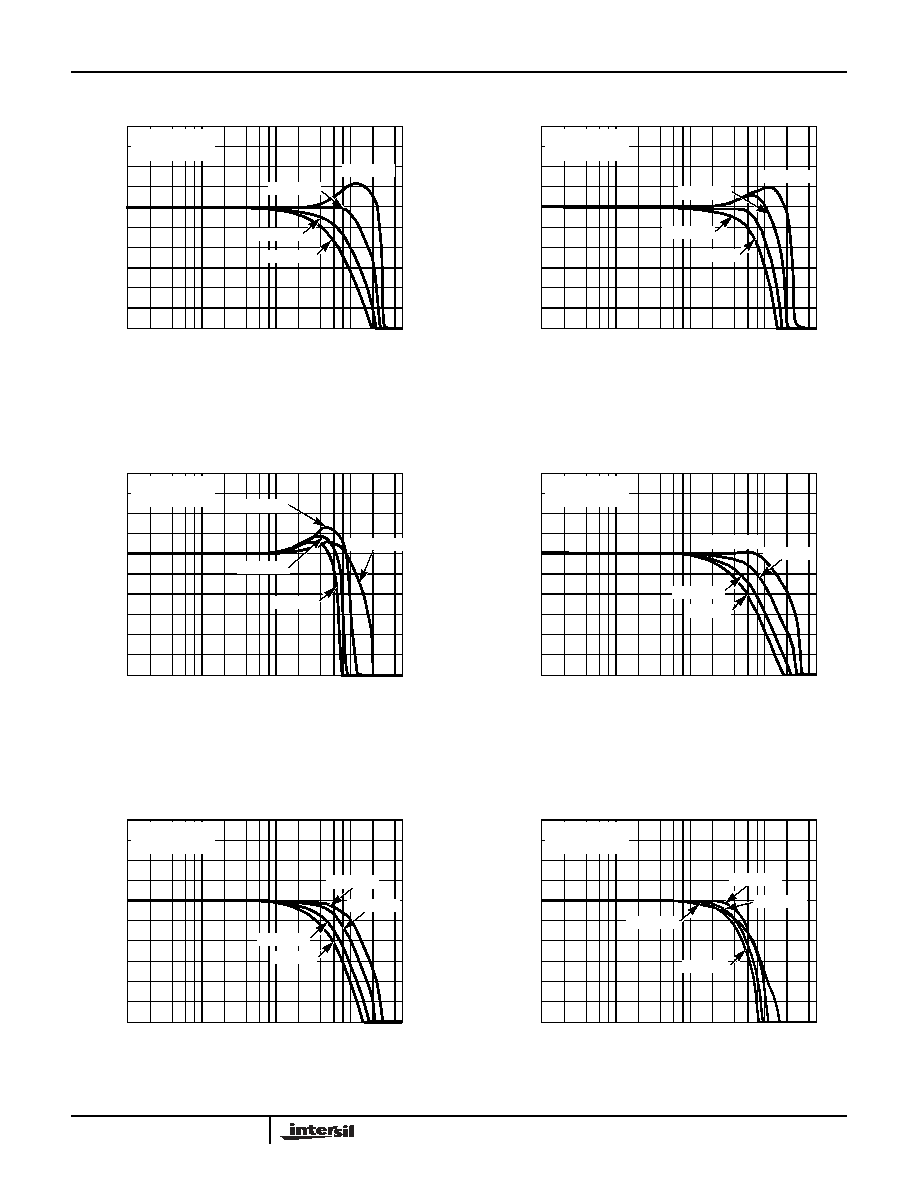
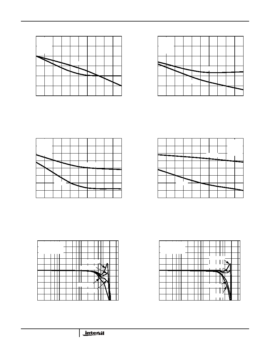
Typical Performance Curves
FIGURE 1. DIFFERENTIAL FREQUENCY RESPONSE WITH
VARIOUS R
F
(FULL POWER MODE)
FIGURE 2. DIFFERENTIAL FREQUENCY RESPONSE WITH
VARIOUS R
F
(3/4 POWER MODE)
FIGURE 3. DIFFERENTIAL FREQUENCY RESPONSE WITH
VARIOUS R
F
(1/2 POWER MODE)
FIGURE 4. DIFFERENTIAL FREQUENCY RESPONSE WITH
VARIOUS R
F
(FULL POWER MODE)
FIGURE 5. DIFFERENTIAL FREQUENCY RESPONSE WITH
VARIOUS R
F
(3/4 POWER MODE)
FIGURE 6. DIFFERENTIAL FREQUENCY RESPONSE WITH
VARIOUS R
F
(1/2 POWER MODE)
R
F
= 1k
R
F
= 750
R
F
= 243
R
F
= 500
22
20
18
16
14
12
10
8
6
4
2
100K
1M
10M
100M
500M
FREQUENCY (Hz)
G
A
IN
(
d
B)
V
S
= ±6V, A
V
= 5
R
L
= 100
DIFF
R
F
= 1k
R
F
= 750
R
F
= 243
22
20
18
16
14
12
10
8
6
4
2
100K
1M
10M
100M
500M
FREQUENCY (Hz)
G
A
IN
(
d
B)
V
S
= ±6V, A
V
= 5
R
L
= 100
DIFF
R
F
= 500
RF = 750
RF = 243
22
20
18
16
14
12
10
8
6
4
2
100K
1M
10M
100M
500M
FREQUENCY (Hz)
GA
IN (
d
B)
VS = ±6V, AV = 5
RL = 100
DIFF
RF = 500
RF = 1k
R
F
= 1k
R
F
= 243
R
F
= 500
28
26
24
22
20
18
16
14
12
10
8
100K
1M
10M
100M
500M
FREQUENCY (Hz)
GA
IN (
d
B)
V
S
= ±6V, A
V
= 10
R
L
= 100
DIFF
R
F
= 750
R
F
= 1k
R
F
= 243
R
F
= 500
28
26
24
22
20
18
16
14
12
10
8
100K
1M
10M
100M
500M
FREQUENCY (Hz)
G
A
IN
(
d
B)
V
S
= ±6V, A
V
= 10
R
L
= 100
DIFF
R
F
= 750
R
F
= 1k
R
F
= 243
R
F
= 500
28
26
24
22
20
18
16
14
12
10
8
100K
1M
10M
100M
500M
FREQUENCY (Hz)
G
A
IN
(
d
B)
V
S
= ±6V, A
V
= 10
R
L
= 100
DIFF
R
F
= 750
EL8108
4
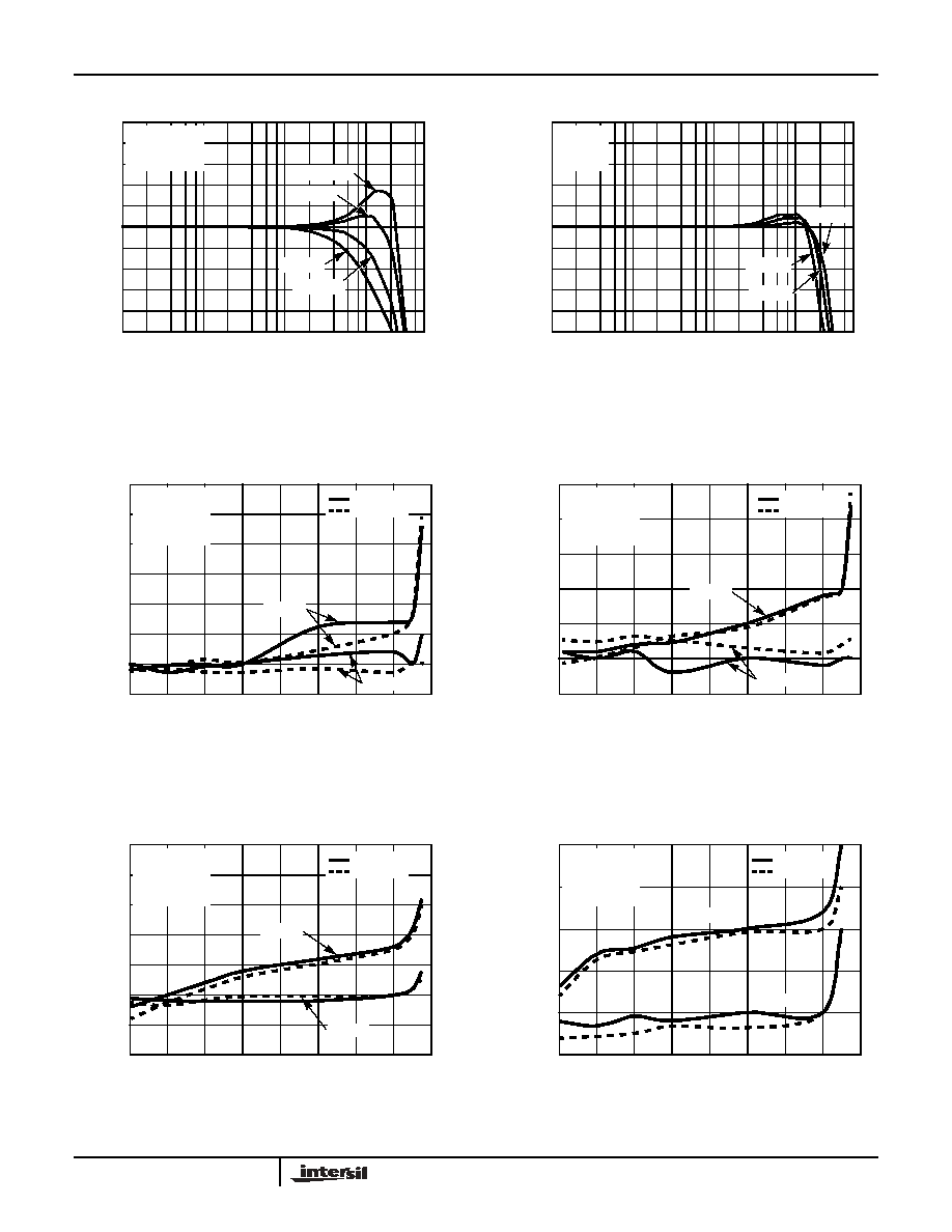
FIGURE 7. DIFFERENTIAL FREQUENCY RESPONSE WITH
VARIOUS R
F
FIGURE 8. FREQUENCY RESPONSE FOR VARIOUS R
LOAD
FIGURE 9. DISTORTION BETWEEN EL8108IL vs EL8108IS
AT 2MHz
FIGURE 10. DISTORTION BETWEEN EL8108IL vs EL8108IS
AT 3MHz
FIGURE 11. DISTORTION BETWEEN EL8108IL vs EL8108IS
AT 5MHz
FIGURE 12. DISTORTION BETWEEN EL8108IL vs EL8108IS
AT 10MHz
Typical Performance Curves
(Continued)
-2
0
2
4
6
8
10
100K
1M
10M
100M
500M
FREQUENCY (Hz)
G
A
IN
(
d
B)
V
S
=±6V
A
V
=2
R
L
=100
DIFF
14
12
R
F
=1k
R
F
=750
R
F
=248
R
F
=500
-8
-6
-4
-2
0
2
4
100K
1M
10M
100M
500M
FREQUENCY (Hz)
NORMALIZ
E
D
GAIN
(dB)
V
S
=±6V
A
V
=2
R
F
=500
8
6
R
L
=150
R
L
=50
R
L
=25
-85
-80
-75
-70
-65
-60
-55
-50
1
2
3
4
5
6
7
8
9
V
OP-P
(V)
HD (
d
B
)
EL8108IL
EL8108IS
3rd HD
2nd HD
V
S
=±6V
A
V
=5
R
L
=50
DIFF
R
F
=750
-80
-75
-70
-65
-60
-55
-50
1
2
3
4
5
6
7
8
9
V
OP-P
(V)
HD (
d
B
)
EL8108IL
EL8108IS
3rd HD
2nd HD
V
S
=±6V
A
V
=5
R
L
=50
DIFF
R
F
=750
-75
-65
-60
-55
-50
-45
-40
1
2
3
4
5
6
7
8
9
V
OP-P
(V)
HD
(
d
B
)
EL8108IL
EL8108IS
3rd HD
V
S
=±6V
A
V
=5
R
L
=50
DIFF
R
F
=750
-70
2nd HD
-65
-60
-55
-50
-45
-40
1
2
3
4
5
6
7
8
9
V
OP-P
(V)
HD
(
d
B
)
EL8108IL
EL8108IS
3rd HD
V
S
=±6V
A
V
=5
R
L
=50
DIFF
R
F
=750
2nd HD
EL8108
5
FIGURE 13. 2nd AND 3rd HARMONIC DISTORTION vs R
LOAD
@ 2MHz (EL8108IL)
FIGURE 14. 2nd AND 3rd HARMONIC DISTORTION vs R
LOAD
@ 3MHz (EL8108IL)
FIGURE 15. 2nd AND 3rd HARMONIC DISTORTION vs R
LOAD
@ 5MHz (EL8108IL)
FIGURE 16. 2nd AND 3rd HARMONIC DISTORTION vs R
LOAD
@ 10MHz (EL8108IL)
FIGURE 17. FREQUENCY RESPONSE WITH VARIOUS C
L
FIGURE 18. FREQUENCY RESPONSE vs VARIOUS C
L
(3/4 POWER MODE)
Typical Performance Curves
(Continued)
-100
-95
-90
-85
-80
-75
-70
50
60
70
80
90
100
110
120
150
R
LOAD
(
)
HD
(dB)
3rd HD
2nd HD
V
S
=±6V
A
V
=5
R
F
=750
V
OPP
=4V
130
140
-90
-85
-80
-75
-70
-65
-60
50
60
70
80
90
100
110
120
150
R
LOAD
(
)
HD
(dB)
2nd HD
V
S
=±6V
A
V
=5
R
F
=750
V
OPP
=4V
130
140
3rd HD
-90
-85
-80
-75
-70
-65
-60
50
60
70
80
90
100
110
120
150
R
LOAD
(
)
HD (dB)
2nd HD
130
140
3rd HD
-55
-50
V
S
=±6V
A
V
=5
R
F
=750
V
OPP
=4V
-80
-75
-70
-65
-60
-55
-50
50
60
70
80
90
100
110
120
150
R
LOAD
(
)
HD (dB)
2nd HD
130
140
-45
-40
V
S
=±6V
A
V
=5
R
F
=750
V
OPP
=4V
3rd HD
C
L
= 47pF
22
20
18
16
14
12
10
8
6
0
100K
1M
10M
100M
500M
FREQUENCY (Hz)
GAI
N
(
d
B)
V
S
= ±6V, A
V
= 5
R
L
= 50
C
L
= 22pF
R
F
= 750
C
L
= 33pF
C
L
= 0pF
24
22
20
18
16
14
12
10
8
6
4
100K
1M
10M
100M
500M
FREQUENCY (Hz)
GAI
N
(
d
B)
V
S
= ±6V, A
V
= 5
R
L
= 50
R
F
= 750
C
L
= 0pF
C
L
= 39pF
C
L
= 47pF
C
L
= 12pF
EL8108