Äîêóìåíòàöèÿ è îïèñàíèÿ www.docs.chipfind.ru
1
®
FN6293.0
CAUTION: These devices are sensitive to electrostatic discharge; follow proper IC Handling Procedures.
1-888-INTERSIL or 1-888-468-3774
|
Intersil (and design) is a registered trademark of Intersil Americas Inc.
Copyright © Intersil Americas Inc. 2005. All Rights Reserved.
All other trademarks mentioned are the property of their respective owners.
EL8171, EL8172
Micropower, Single Supply, Rail-to-Rail
Input-Output Instrumentation Amplifiers
The EL8171 and EL8172 are micropower instrumentation
amplifiers optimized for operation at 2.9V to 5V single
supplies. Inputs and outputs can operate rail-to-rail. As with
all instrumentation amplifiers, a pair of inputs provide very
high common-mode rejection and are completely
independent from a pair of feedback terminals. The
feedback terminals allow zero input to be translated to any
output offset, including ground. A feedback divider controls
the overall gain of the amplifier.
The EL8172 is compensated for a gain of 100 or more, and
the EL8171 is compensated for a gain of 10 or more. The
EL8171 and EL8172 have PMOS input devices that provide
sub-nA input bias currents.
The amplifiers can be operated from one lithium cell or two
Ni-Cd batteries. The EL8171 and EL8172 input range goes
from below ground to slightly above positive rail. The output
stage swings completely to ground or positive supply - no
pull-up or pull-down resistors are needed.
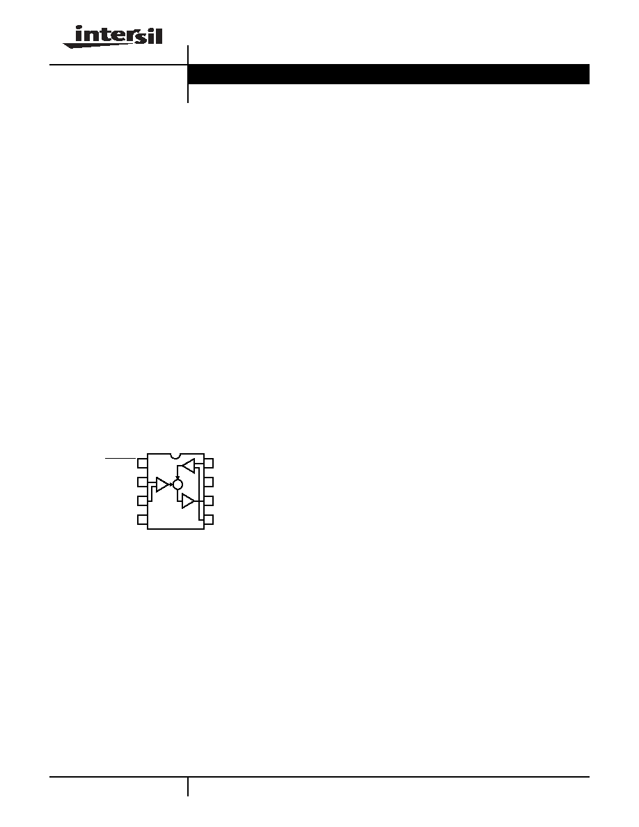
Pinout
EL8171, EL8172
(8 LD SO)
TOP VIEW
Features
· 78µA maximum supply current
· Maximum input offset voltage
- 300µV (EL8172)
- 1000µV (EL8171)
· 200pA maximum input bias current
· 3µV/°C offset voltage drift
· 450kHz -3dB bandwidth (G = 10)
· 170kHz -3dB bandwidth (G = 100)
· 0.5V/µs slew rate
· Single supply operation
- Input voltage range is rail-to-rail
- Output swings rail-to-rail
· Output sources and sinks ±29mA load current
· 0.2% gain accuracy
· Pb-free plus anneal available (RoHS compliant)
Applications
· Battery- or solar-powered systems
· Strain gauges
· Current monitors
· Thermocouple amplifiers
1
2
3
4
8
7
6
5
+
-
+
-
ENABLE
IN-
IN+
VS-
FB+
VS+
FB-
OUT
Data Sheet
October 26, 2005
2
FN6293.0
October 26, 2005
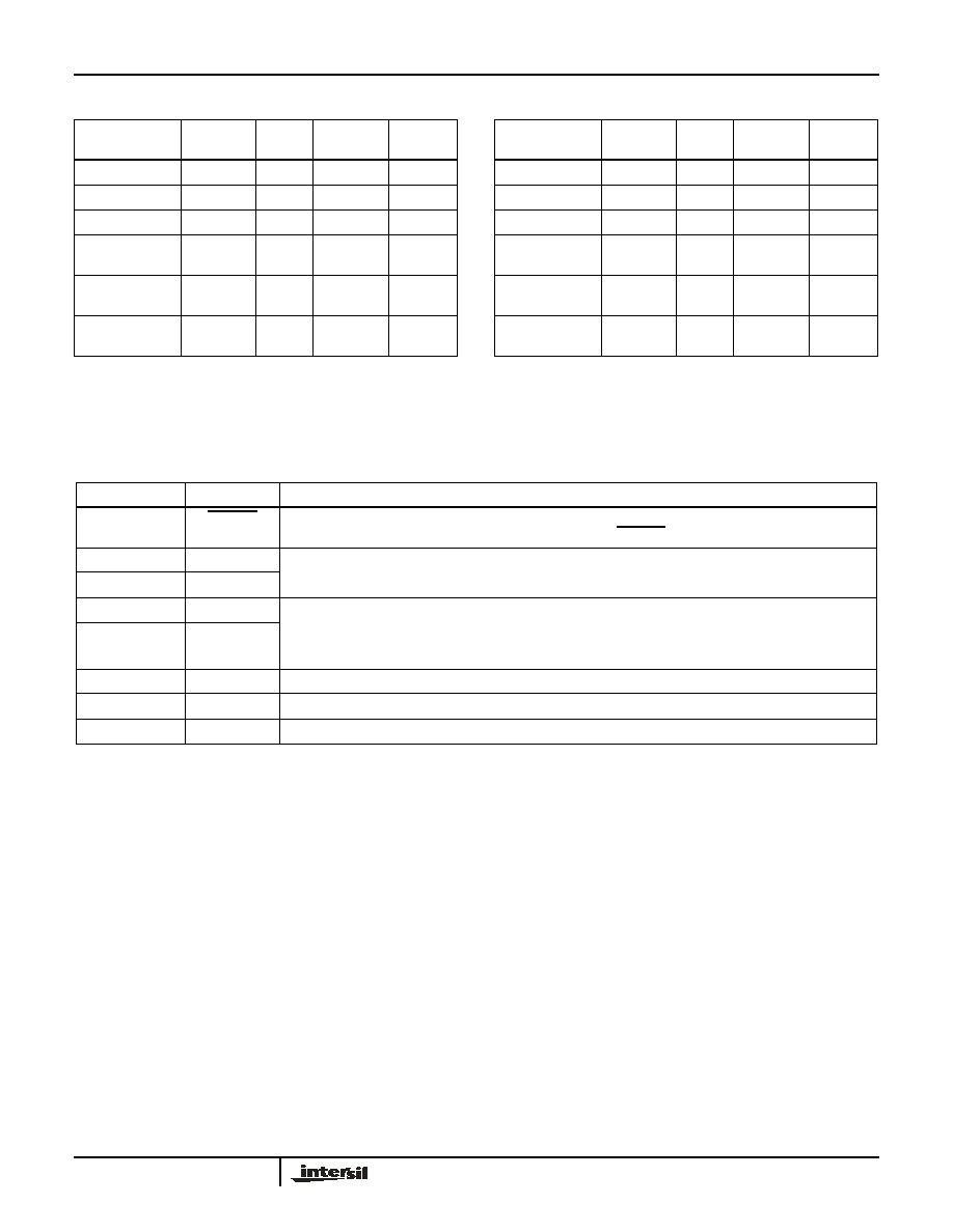
Ordering Information
PART NUMBER
PART
MARKING
TAPE &
REEL
PACKAGE
PKG.
DWG. #
PART NUMBER
PART
MARKING
TAPE &
REEL
PACKAGE
PKG.
DWG. #
EL8171IS
8171IS
-
8 Ld SO
MDP0027
EL8172IS
8172IS
-
8 Ld SO
MDP0027
EL8171IS-T7
8171IS
7"
8 Ld SO
MDP0027
EL8172IS-T7
8172IS
7"
8 Ld SO
MDP0027
EL8171IS-T13
8171IS
13"
8 Ld SO
MDP0027
EL8172IS-T13
8172IS
13"
8 Ld SO
MDP0027
EL8171ISZ
(See Note)
8171ISZ
-
8 Ld SO
(Pb-free)
MDP0027
EL8172ISZ
(See Note)
8172ISZ
-
8 Ld SO
(Pb-free)
MDP0027
EL8171ISZ-T7
(See Note)
8171ISZ
7"
8 Ld SO
(Pb-free)
MDP0027
EL8172ISZ-T7
(See Note)
8172ISZ
7"
8 Ld SO
(Pb-free)
MDP0027
EL8171ISZ-T13
(See Note)
8171ISZ
13"
8 Ld SO
(Pb-free)
MDP0027
EL8172ISZ-T13
(See Note)
8172ISZ
13"
8 Ld SO
(Pb-free)
MDP0027
NOTE: Intersil Pb-free plus anneal products employ special Pb-free material sets; molding compounds/die attach materials and 100% matte tin plate
termination finish, which are RoHS compliant and compatible with both SnPb and Pb-free soldering operations. Intersil Pb-free products are MSL
classified at Pb-free peak reflow temperatures that meet or exceed the Pb-free requirements of IPC/JEDEC J STD-020.
Pin Description
EL8171/EL8172
PIN NAME
PIN FUNCTION
1
ENABLE
Active Low. When pulled up above 2V, the in-amp conserves 3µA disabled supply current and the output is
in a high impedance state. An internal pull down defines the ENABLE low when left floating.
2
IN-
Inverting (IN-) and non-inverting (IN+) high impedance input terminals. The input terminals are equivalent to
the gate of PMOS transistor.
3
IN+
5
FB-
High impedance feedback terminals. The feedback terminals have a very similar equivalent circuit as the
input terminals. The negative feedback (FB-) pin connects to an external resistive network to set the gain of
the in-amp. The positive feedback (FB+) pin can be used to shift the DC level of the output or as an output
offset.
8
FB+
7
VS+
Positive supply terminal.
4
VS-
Negative supply terminal.
6
VOUT
Output Voltage.
EL8171, EL8172
3
FN6293.0
October 26, 2005
Absolute Maximum Ratings
(T
A
= 25°C)
Supply Voltage, V
S
. . . . . . . . . . . . . . . . . . . . . . . . . . . . . . . . . . 5.5V
Differential Input Current . . . . . . . . . . . . . . . . . . . . . . . . . . . . . . 5mA
Differential Input Voltage . . . . . . . . . . . . . . . . . . . . . . . . . . . . . . . .5V
V
EN
. . . . . . . . . . . . . . . . . . . . . . . . . . . . . . . . . . .0.5V to V
S
+ + 0.5V
ESD . . . . . . . . . . . . . . . . . . . . . . . . . . . . . . . . . . . . . . . . . . . . . . .3kV
Output Short-Circuit Duration . . . . . . . . . . . . . . . . . . . . . . .Indefinite
Ambient Operating Temperature . . . . . . . . . . . . . . . .-40°C to +85°C
Storage Temperature . . . . . . . . . . . . . . . . . . . . . . . .-65°C to +150°C
CAUTION: Stresses above those listed in "Absolute Maximum Ratings" may cause permanent damage to the device. This is a stress only rating and operation of the
device at these or any other conditions above those indicated in the operational sections of this specification is not implied.
IMPORTANT NOTE: All parameters having Min/Max specifications are guaranteed. Typical values are for information purposes only. Unless otherwise noted, all tests
are at the specified temperature and are pulsed tests, therefore: T
J
= T
C
= T
A
Electrical Specifications
V
S
+ = +5V, V
S
- = GND, VCM = 1/2V
S
+ T
A
= 25°C, unless otherwise specified.
PARAMETER
DESCRIPTION
CONDITIONS
MIN
TYP
MAX
UNIT
V
OS
Input Offset Voltage
EL8171
400
1000
µV
EL8172
150
300
µV
TCV
OS
Input Offset Voltage Temperature
Coefficient
Temperature = -40°C to 85°C
3
µV/°C
I
OS
Input Offset Current
10
200
pA
I
B
Input Bias Current
10
200
pA
e
N
Input Noise Voltage
EL8171
f = 0.1Hz to 10Hz
10
µV
P-P
EL8172
4
µV
P-P
Input Noise Voltage Density
f
o
= 1kHz
50
nV/
Hz
R
IN
Input Resistance
25
G
V
IN
Input Voltage Range
Guaranteed by CMRR test
0
5
V
CMRR
Common Mode Rejection Ratio
EL8172, V
CM
= 0V to +5V
80
108
dB
EL8171, V
CM
= 0V to +5V
80
104
dB
PSRR
Power Supply Rejection Ratio
EL8172, V
S
= 2.4V to 5V
80
104
dB
EL8171, V
S
= 2.4V to 5V
70
90
dB
E
G
Gain Error
EL8172, R
L
= 100k
to 2.5V
-1.5
+0.3
+1.5
%
EL8171, R
L
= 100k
to 2.5V
-0.8
+0.2
+0.8
%
V
OUT
Maximum Voltage Swing
Output low, 100k
to 2.5V
0
4
10
mV
Output low, 1k
to 2.5V
0.13
0.25
V
Output high, 100k
to 2.5V
4.990
4.996
V
Output high, 1k
to GND
4.75
4.88
V
SR
Slew Rate
R
L
= 1k
to GND
0.3
0.5
0.7
V/µs
-3dB BW
-3dB Bandwidth
EL8171
Gain = 10V/V
450
kHz
Gain = 20
210
kHz
Gain = 50
66
kHz
Gain = 100
33
kHz
EL8172
Gain = 100
172
kHz
Gain = 200
70
kHz
Gain = 500
25
kHz
Gain = 1000
12
kHz
I
S,EN
Supply Current, Enabled
40
60
78
µA
EL8171, EL8172
4
FN6293.0
October 26, 2005
I
S,DIS
Supply Current, Disabled
EN = V
S
+
1.5
2.9
5
µA
V
ENH
Enable Pin for Shut-down
2
V
V
ENL
Enable Pin for Power-on
0.8
V
V
S
Minimum Supply Voltage
2.2
2.4
V
I
O
Output Current into 10
to V
S
/2
V
S
= 5V
±18
±29
mA
V
S
= 2.9V
±4
±7.5
mA
Electrical Specifications
V
S
+ = +5V, V
S
- = GND, VCM = 1/2V
S
+ T
A
= 25°C, unless otherwise specified. (Continued)
PARAMETER
DESCRIPTION
CONDITIONS
MIN
TYP
MAX
UNIT
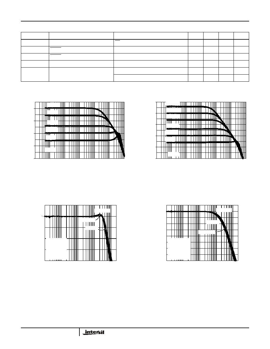
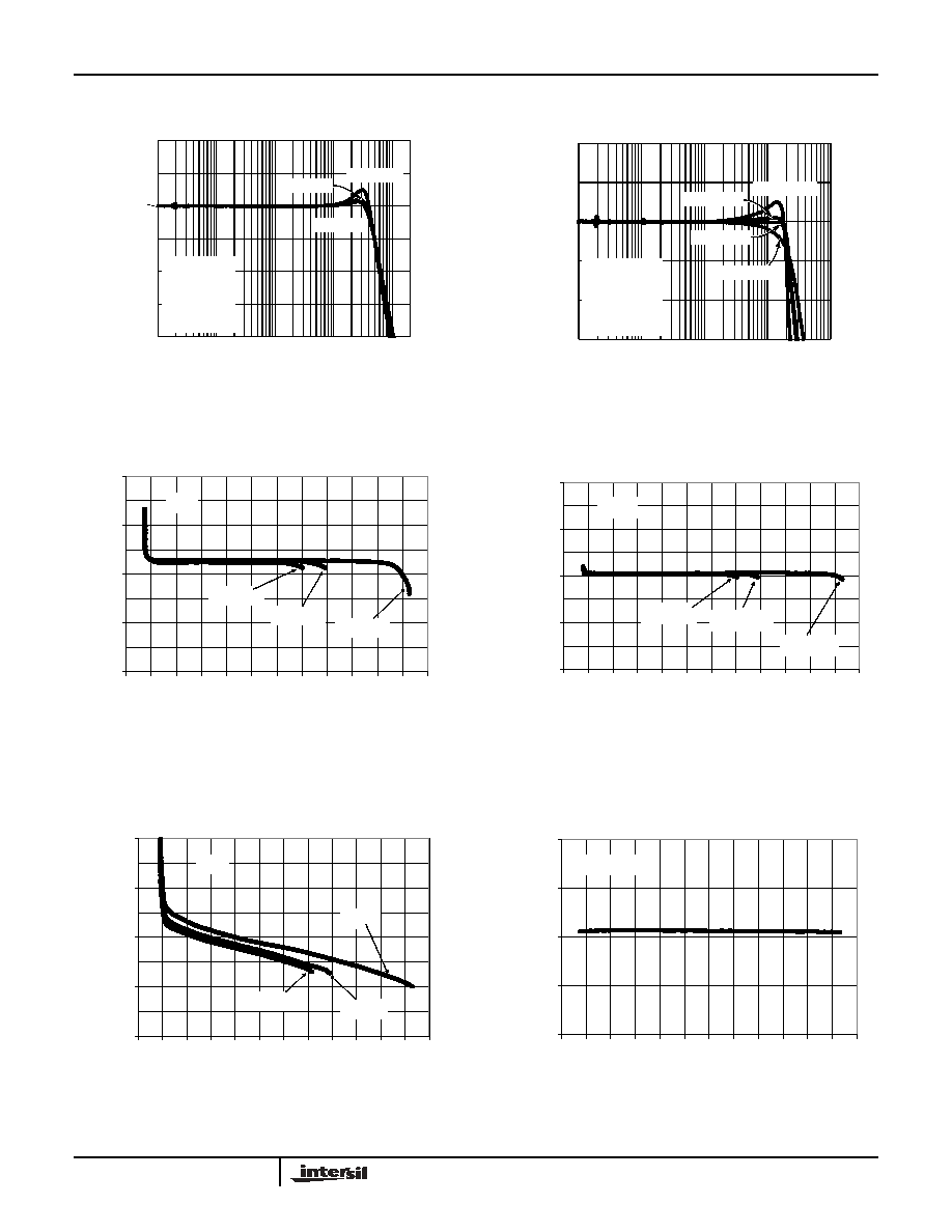
Typical Performance Curves
FIGURE 1. EL8171 FREQUENCY RESPONSE vs CLOSED
LOOP GAIN
FIGURE 2. EL8172 FREQUENCY RESPONSE vs CLOSED
LOOP GAIN
FIGURE 3. EL8171 FREQUENCY RESPONSE vs SUPPLY
VOLTAGE
FIGURE 4. EL8172 FREQUENCY RESPONSE vs SUPPLY
VOLTAGE
0
10
20
30
40
FREQUENCY (Hz)
GAIN (d
B)
G=5
G=10
G=20
G=50
G=100
Vs=5V
1
10
100
1K
10K
100K
1M
20
30
40
50
60
70
FREQUENCY (Hz)
GAIN (dB)
G=50
G=100
G=200
G=500
G=1000
Vs=5V
1
10
100
1K
10K
100K
1M
G=2000
100
10k
1k
100k
25
20
15
10
5
0
FREQUENCY (Hz)
GAI
N
(d
B)
A
V
=10
R
L
=10k
C
L
=10pF
R
F
/R
G
=9.08
R
F
=178k
R
G
=19.6k
1M
V
S
=±1.25V
V
S
=±2.5V
V
S
=±1V
100
10k
1k
100k
45
40
30
20
10
0
FREQUENCY (Hz)
MAGNIT
UDE
(dB)
1M
35
25
15
5
V
S
=±1.25V
V
S
=±1V
V
S
=±2.5V
A
V
=100
R
L
=10k
C
L
=10pF
R
F
/R
G
=99.02
R
F
=221k
R
G
=2.23k
EL8171, EL8172
5
FN6293.0
October 26, 2005
FIGURE 5. EL8171 FREQUENCY RESPONSE vs C
LOAD
FIGURE 6. EL8172 FREQUENCY RESPONSE vs C
LOAD
FIGURE 7. EL8171 AND EL8172 AVERAGE INPUT BIAS
CURRENT vs COMMON-MODE INPUT VOLTAGE
@ 25°C
FIGURE 8. EL8171 AND EL8172 AVERAGE INPUT BIAS
CURRENT vs COMMON-MODE INPUT VOLTAGE
@ -45°C
FIGURE 9. EL8171 AND EL8172 AVERAGE INPUT BIAS
CURRENT vs COMMON-MODE INPUT VOLTAGE
@ 85°C
FIGURE 10. EL8171 AND EL8172 INPUT OFFSET CURRENT
vs COMMON-MODE INPUT VOLTAGE
Typical Performance Curves
(Continued)
100
10k
1k
100k
30
25
20
15
10
0
FREQUENCY (Hz)
MAGNITUDE (
d
B)
A
V
=10
V
S
=5V
R
L
=10k
R
F
/R
G
=9.08
R
F
=178k
R
G
=19.6k
1M
5
C
L
=100pF
C
L
=27pF
C
L
=47pF
100
10k
1k
100k
50
45
40
35
30
25
FREQUENCY (Hz)
MA
GNITUDE (dB)
A
V
=100
V
S
=5V
R
L
=10k
R
F
/R
G
=99.02
R
F
=221k
R
G
=2.23k
1M
C
L
=2200pF
C
L
=1000pF
C
L
=820pF
C
L
=390pF
-4
-2
0
2
4
-0.5
0
0.5
1
1.5
2
2.5
3
3.5
4
4.5
5
5.5
COMMON-MODE INPUT VOLTAGE (V)
AV
ERA
G
E I
N
PU
T BI
AS
CUR
REN
T
(pA)
25C
Vs=2.9V
Vs=3.3V
Vs=5V
25°C
-4
-2
0
2
4
-0.5
0
0.5
1
1.5
2
2.5
3
3.5
4
4.5
5
5.5
COMMON-MODE INPUT VOLTAGE (V)
A
VERA
G
E I
N
PU
T BI
AS
CURR
ENT
(pA)
-45C
Vs=2.9V
Vs=3.3V
Vs=5V
-45°C
-100
-50
0
50
100
-0.5 0
0.5
1
1.5
2
2.5
3
3.5
4
4.5
5
5.5
COMMON-MODE INPUT VOLTAGE (V)
AVER
AGE I
N
P
U
T B
I
A
S
CUR
REN
T
(pA)
85C
Vs=5V
Vs=3.3V
Vs=2.9V
85°C
-10
-5
0
5
10
-0.5
0
0.5
1
1.5
2
2.5
3
3.5
4
4.5
5
5.5
COMMON-MODE INPUT VOLTAGE (V)
I
N
P
U
T OF
FS
ET
C
URR
ENT
(pA)
Vs=5V
EL8171, EL8172