Äîêóìåíòàöèÿ è îïèñàíèÿ www.docs.chipfind.ru
1
®
FN7436.2
PRELIMINARY
EL8176
Micropower Single Supply Rail-to-Rail
Input-Output Precision Op Amp
The EL8176 is a micropower precision operational amplifier
optimized for single supply operation at 5V and can operate
down to 2.4V.
The EL8176 draws minimal supply current while meeting
excellent DC-accuracy noise and output drive specifications.
Competing devices seriously degrade these parameters to
achieve micropower supply current. Offset current, voltage
and current noise, slew rate, and gain-bandwidth product are
all two to ten times better than on previous micropower op
amps.
The EL8176 can be operated from one lithium cell or two
Ni-Cd batteries. The input range includes both positive and
negative rail. The output swings to both rails.
Features
· 55µA supply current
· 100µV max offset voltage
· 500pA input bias current
· 400kHz gain-bandwidth product
· 1MHz -3dB bandwidth
· 0.13V/µs slew rate
· Single supply operation down to 2.4V
· Rail-to-rail input and output
· Output sources and sinks 26mA load current
· Pb-free plus anneal available (RoHS compliant)
Applications
· Battery- or solar-powered systems
· 4mA to 20mA current loops
· Handheld consumer products
· Medical devices
· Thermocouple amplifiers
· Photodiode pre amps
· pH probe amplifiers
Pinouts
EL8176
(6 LD SOT-23)
TOP VIEW
EL8176
(8 LD SO)
TOP VIEW
Ordering Information
PART NUMBER
PART
MARKING
PACKAGE
TAPE &
REEL
PKG.
DWG. #
EL8176AIW-T7
BBGA
6 Ld SOT-23
7"
(3K pcs)
MDP0038
EL8176AIW-T7A
BBGA
6 Ld SOT-23
7"
(250 pcs)
MDP0038
EL8176AIWZ-T7
(Note)
BBNA
6 Ld SOT-23
(Pb-free)
7"
(3K pcs)
MDP0038
EL8176AIWZ-T7A
(Note)
BBNA
6 Ld SOT-23
(Pb-free)
7"
(250 pcs)
MDP0038
EL8176BIW-T7
BBGA
6 Ld SOT-23
7"
(3K pcs)
MDP0038
EL8176BIW-T7A
BBGA
6 Ld SOT-23
7"
(250 pcs)
MDP0038
EL8176BIWZ-T7
(Note)
BBNA
6 Ld SOT-23
(Pb-free)
7"
(3K pcs)
MDP0038
EL8176BIWZ-T7A
(Note)
BBNA
6 Ld SOT-23
(Pb-free)
7"
(250 pcs)
MDP0038
EL8176ISZ
(Note)
8176ISZ
8 Ld SO
(Pb-free)
-
MDP0027
EL8176ISZ-T7
(Note)
8176ISZ
8 Ld SO
(Pb-free)
7"
MDP0027
EL8176ISZ-T13
(Note)
8176ISZ
8 Ld SO
(Pb-free)
13"
MDP0027
NOTE: Intersil Pb-free plus anneal products employ special Pb-free
material sets; molding compounds/die attach materials and 100% matte
tin plate termination finish, which are RoHS compliant and compatible
with both SnPb and Pb-free soldering operations. Intersil Pb-free
products are MSL classified at Pb-free peak reflow temperatures that
meet or exceed the Pb-free requirements of IPC/JEDEC J STD-020.
1
2
3
6
4
5
+ -
OUT
VS-
IN+
VS+
ENABLE
IN-
1
2
3
4
8
7
6
5
-
+
NC
IN-
IN+
ENABLE
VS+
VOUT
VS-
NC
Data Sheet
October 5, 2005
CAUTION: These devices are sensitive to electrostatic discharge; follow proper IC Handling Procedures.
1-888-INTERSIL or 1-888-468-3774
|
Intersil (and design) is a registered trademark of Intersil Americas Inc.
Copyright Intersil Americas Inc. 2004, 2005. All Rights Reserved
All other trademarks mentioned are the property of their respective owners.
2
FN7436.2
October 5, 2005
Absolute Maximum Ratings
(T
A
= 25°C)
Supply Voltage . . . . . . . . . . . . . . . . . . . . . . . . . . . . . . . . . . . . . . 5.5V
Differential Input Current . . . . . . . . . . . . . . . . . . . . . . . . . . . . . . 5mA
Input Voltage . . . . . . . . . . . . . . . . . . . . . . . . . . . . -0.5V to V
S
+ 0.5V
Output Short-Circuit Duration . . . . . . . . . . . . . . . . . . . . . . .Indefinite
Ambient Operating Temperature Range . . . . . . . . . .-40°C to +85°C
Storage Temperature Range . . . . . . . . . . . . . . . . . .-65°C to +150°C
Operating Junction Temperature . . . . . . . . . . . . . . . . . . . . . . . 125°C
CAUTION: Stresses above those listed in "Absolute Maximum Ratings" may cause permanent damage to the device. This is a stress only rating and operation of the
device at these or any other conditions above those indicated in the operational sections of this specification is not implied.
IMPORTANT NOTE: All parameters having Min/Max specifications are guaranteed. Typical values are for information purposes only. Unless otherwise noted, all tests
are at the specified temperature and are pulsed tests, therefore: T
J
= T
C
= T
A
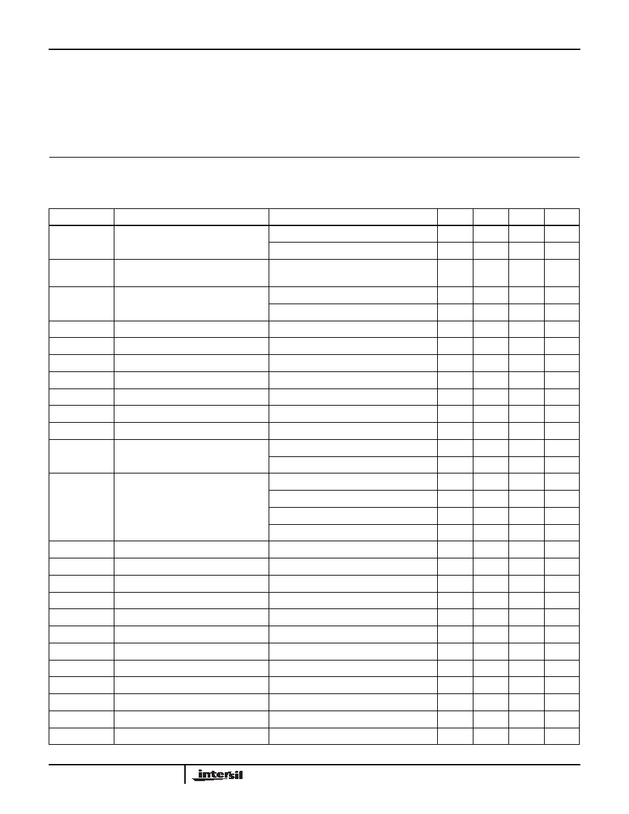
Electrical Specifications
V
S
= 5V, 0V, V
CM
= 0.1V, V
O
= 1.4V, T
A
= 25°C unless otherwise specified.
PARAMETER
DESCRIPTION
CONDITIONS
MIN
TYP
MAX
UNIT
V
OS
Input Offset Voltage
Grade A
50
100
µV
Grade B
110
400
µV
Long Term Input Offset Voltage Stability
TBD
µV/Mo
Input Offset Drift vs Temperature
EL8176IW
0.7
µV/°C
EL8176IS
0.3
µV/°C
I
OS
Input Offset Current
0.4
1.2
nA
I
B
Input Bias Current
0.5
2
nA
e
N
Input Noise Voltage Density
f
O
= 1kHz
25
nV/
Hz
i
N
Input Noise Current Density
f
O
= 1kHz
0.1
pA/
Hz
CMIR
Input Voltage Range
Guaranteed by CMRR test
0
5
V
CMRR
Common-Mode Rejection Ratio
V
CM
= 0V to 5V
90
110
dB
PSRR
Power Supply Rejection Ratio
V
S
= 2.4V to 5V
90
110
dB
A
VOL
Large Signal Voltage Gain
V
O
= 0.5V to 4.5V, R
L
= 100k
200
500
V/mV
V
O
= 0.5V to 4.5V, R
L
= 1k
25
V/mV
V
OUT
Maximum Output Voltage Swing
Output low, R
L
= 100k
3
6
mV
Output low, R
L
= 1k
130
200
mV
Output high, R
L
= 100k
4.994
4.997
V
Output high, R
L
= 1k
4.8
4.88
V
SR
Slew Rate
0.09
0.13
0.17
V/µs
GBW
Gain Bandwidth Product
f
O
= 100kHz
400
kHz
BW
-3dB Bandwidth
Unity gain, C
LOAD
= 27pF, R
F
= 100
1
MHz
I
S,ON
Supply Current, Enabled
40
55
75
µA
I
S,OFF
Supply Current, Disabled
3
10
µA
I
O
+
Short Circuit Output Current
R
L
= 10
18
31
mA
I
O
-
Short Circuit Output Current
R
L
= 10
17
26
mA
V
S
Minimum Supply Voltage
2.2 2.4 V
V
INH
Enable Pin High Level
2
V
V
INL
Enable Pin Low Level
0.8
V
I
ENH
Enable Pin Input Current
V
EN
= 5V
0.25
0.7
2
µA
I
ENL
Enable Pin Input Current
V
EN
= 0V
-0.5
0
+0.5
µA
V
OS
Time
------------------
V
OS
T
----------------
EL8176
3
FN7436.2
October 5, 2005
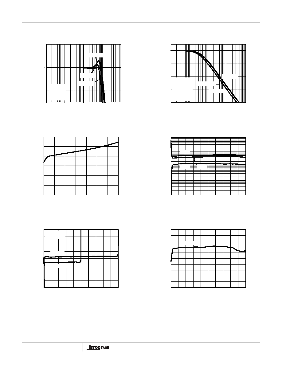
Typical Performance Curves
FIGURE 1. UNITY GAIN FREQUENCY RESPONSE vs
SUPPLY VOLTAGE
FIGURE 2. FREQUENCY RESPONSE vs SUPPLY VOLTAGE
FIGURE 3. SUPPLY CURRENT vs SUPPLY VOLTAGE
FIGURE 4. INPUT BIAS + OFFSET CURRENTS vs COMMON-
MODE INPUT VOLTAGE
FIGURE 5. INPUT OFFSET VOLTAGE vs OUTPUT VOLTAGE
FIGURE 6. INPUT OFFSET VOLTAGE vs COMMON-MODE
INPUT VOLTAGE
-6
-3
0
3
6
1K
10K
100K
1M
10M
FREQUENCY (Hz)
G
A
IN (
d
B
)
V
S
=±2.5V
-9
A
V
=1
C
L
=27pF
R
F
=100
R
G
=OPEN
V
S
=±1.25V
V
S
=±1.0V
A
V
=100
R
L
=10k
C
L
=2.7pF
R
F
/R
G
=99.02
R
F
=221k
R
G
=2.23k
0
GAI
N
(
d
B)
15
20
25
40
45
30
35
5
10
100
10K
100K
1M
FREQUENCY (Hz)
1K
V
S
=±1.0V
V
S
=±1.25V
V
S
=±2.5V
2
3.5
4
5.5
SUPPLY VOLTAGE (V)
2.5
5
4.5
3
0
SUP
P
L
Y
CURRENT
(µA)
20
50
60
30
40
10
1
INPUT BIAS, OFFSET CUR
RE
NT
S
(
p
A)
1K
10K
10
100
0
5
COMMON-MODE INPUT VOLTAGE (V)
1
3
2
4
I
B
+
I
OS
I
B
-
-200
I
N
PUT O
F
FS
ET
VOL
T
AGE
(
µ
V
)
-100
0
150
200
50
100
0
5
OUTPUT VOLTAGE (V)
1
3
2
4
V
CM
=V
DD
/2
A
V
=-1
-150
-50
V
DD
=2.5V
V
DD
=5V
-100
I
N
PUT O
F
FS
ET
VOL
T
AGE
(
µ
V
)
-80
-20
0
-60
-40
0
5
COMMON-MODE INPUT VOLTAGE (V)
1
3
2
4
V
OS
, µV
EL8176
4
FN7436.2
October 5, 2005
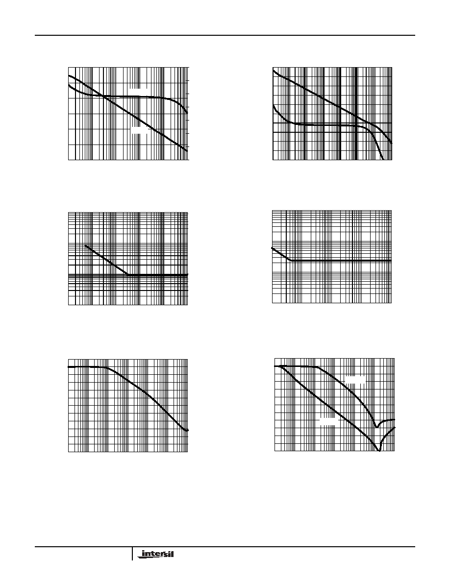
FIGURE 7. A
VOL
vs FREQUENCY @ 1k
LOAD
FIGURE 8. A
VOL
vs FREQUENCY @ 100k
LOAD
FIGURE 9. CURRENT NOISE vs FREQUENCY
FIGURE 10. VOLTAGE NOISE vs FREQUENCY
FIGURE 11. CMRR vs FREQUENCY
FIGURE 12. PSRR vs FREQUENCY
Typical Performance Curves
(Continued)
-20
GA
IN (
d
B)
0
20
80
100
40
60
10
10K
1M
FREQUENCY (Hz)
100
-150
PHASE
(°
)
200
150
100
50
0
-50
-100
100K
1K
PHASE
GAIN
-80
GA
IN (
d
B)
40
120
80
-40
0
1
1K
100K
10M
FREQUENCY (Hz)
10
-120
PHASE
(°
)
80
40
0
-40
-80
10K
1M
100
0.01
0.10
1.00
10.00
1
10
100
1K
10K
FREQUENCY (Hz)
CU
RRE
N
T
NOISE (pA/
Hz
)
100K
1K
100
10
1
10
100
1K
10K
100K
VO
L
T
AGE NOI
SE (nV/
Hz)
FREQUENCY (Hz)
0
10
30
40
50
60
70
80
90
100
110
120
1
10
100
1K
10K
100K
1M
FREQUENCY (Hz)
CMRR (dB)
20
0
10
30
40
50
60
70
80
90
100
110
120
1
10
100
1K
10K
100K
1M
FREQUENCY (Hz)
PSRR (dB)
20
PSRR+
PSRR-
EL8176
5
FN7436.2
October 5, 2005
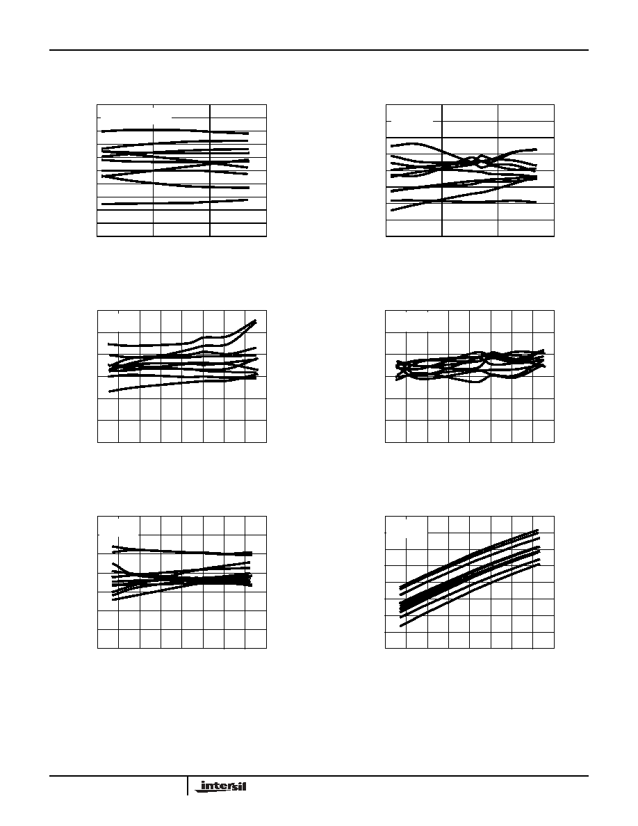
FIGURE 13. V
OS
vs TEMPERATURE
FIGURE 14. PSRR vs TEMPERATURE
FIGURE 15. CMRR vs TEMPERATURE
FIGURE 16. A
VOL
vs TEMPERATURE
FIGURE 17. IB vs TEMPERATURE
FIGURE 18. I
S
vs TEMPERATURE
Typical Performance Curves
(Continued)
-500
-400
-300
-200
-100
0
100
200
300
400
500
-50
0
50
100
TEMPERATURE (°C)
IN
P
U
T OFF
S
E
T
VO
L
T
A
G
E (
µ
V)
SOT23-6 PACKAGE
10 SAMPLES
-50
0
50
100
TEMPERATURE (°C)
90
95
100
105
110
115
120
125
130
P
S
RR (
d
B
)
SOT23-6
PACKAGE
90
95
100
105
110
115
120
-60
-40
-20
0
20
40
60
80
100
TEMPERATURE (°C)
CMRR (
d
B)
SOT23-6
PACKAGE
-60
-40
-20
0
20
40
60
80
100
TEMPERATURE (°C)
100
105
110
115
120
125
130
OP
EN L
O
OP
GAI
N
(
d
B)
SOT23-6
PACKAGE
-60
-40
-20
0
20
40
60
80
100
TEMPERATURE (°C)
-1500
-1000
-500
0
500
1000
1500
2000
IB (
p
A)
SOT23-6
PACKAGE
-60
-40
-20
0
20
40
60
80
100
TEMPERATURE (°C)
30
35
40
45
50
55
60
65
70
I
S
(mA)
SOT23-6
PACKAGE
EL8176