 | ÐлекÑÑоннÑй компоненÑ: EL8300ISZ | СкаÑаÑÑ:  PDF PDF  ZIP ZIP |
Äîêóìåíòàöèÿ è îïèñàíèÿ www.docs.chipfind.ru
1
®
FN7347.2
EL8300
200MHz Rail-to-Rail Amplifier
The EL8300 represents a triple rail-to-rail amplifier with a -
3dB bandwidth of 200MHz and slew rate of 200V/µs.
Running off a very low supply current of 2mA per channel,
the EL8300 also features inputs that go to 0.15V below the
V
S
- rail.
The EL8300 includes a fast-acting disable/power-down
circuit. With a 25ns disable and a 200ns enable, the EL8300
is ideal for multiplexing applications.
The EL8300 is designed for a number of general purpose
video, communication, instrumentation, and industrial
applications. The EL8300 is available in an 16-pin SO and
16-pin QSOP packages and is specified for operation over
the -40°C to +85°C temperature range.
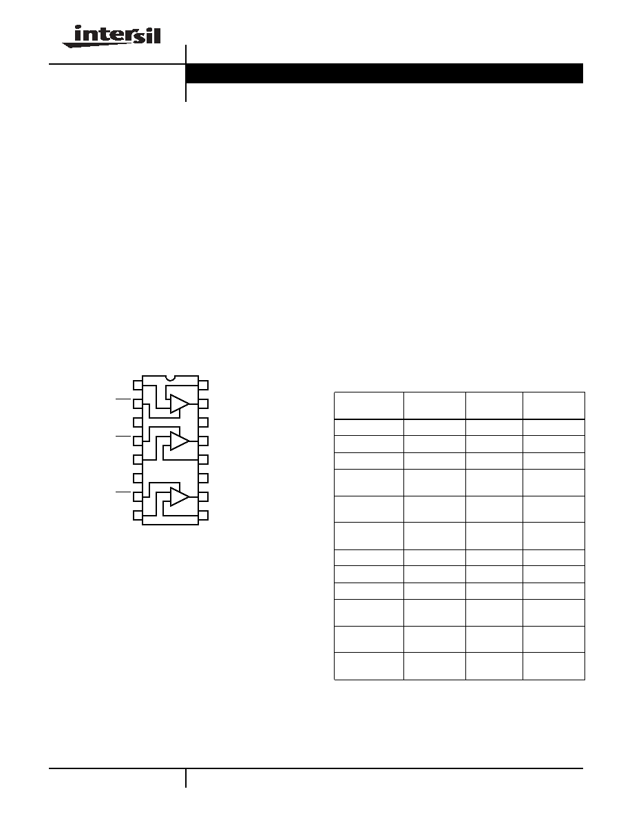
Pinout
EL8300
(16-PIN SO, QSOP)
TOP VIEW
Features
· 200MHz -3dB bandwidth
· 200V/µs slew rate
· Low supply current = 2mA per amplifier
· Supplies from 3V to 5.5V
· Rail-to-rail output
· Input to 0.15V below V
S
-
· Fast 25ns disable
· Low cost
· Pb-Free pus Anneal available (RoHS compliant)
Applications
· Video amplifiers
· Portable/hand-held products
· Communications devices
INA+
CEA
VS-
CEB
INB+
NC
CEC
INC+
INA-
OUTA
VS+
OUTB
INB-
NC
OUTC
INC-
-
+
1
2
3
4
16
15
14
13
5
6
7
12
11
10
8
9
-
+
-
+
Ordering Information
PART
NUMBER
PACKAGE
TAPE & REEL PKG. DWG. #
EL8300IS
16-Pin SO
-
MDP0027
EL8300IS-T7
16-Pin SO
7"
MDP0027
EL8300IS-T13
16-Pin SO
13"
MDP0027
EL8300ISZ
(See Note)
16-Pin SO
(Pb-free)
-
MDP0027
EL8300ISZ-T7
(See Note)
16-Pin SO
(Pb-free)
7"
MDP0027
EL8300ISZ-T13
(See Note)
16-Pin SO
(Pb-free)
13"
MDP0027
EL8300IU
16-Pin QSOP
-
MDP0040
EL8300IU-T7
16-Pin QSOP
7"
MDP0040
EL8300IU-T13
16-Pin QSOP
13"
MDP0040
EL8300IUZ
(See Note)
16-Pin QSOP
(Pb-free)
-
MDP0040
EL8300IUZ-T7
(See Note)
16-Pin QSOP
(Pb-free)
7"
MDP0040
EL8300IUZ-T13
(See Note)
16-Pin QSOP
(Pb-free)
13"
MDP0040
NOTE: Intersil Pb-free products employ special Pb-free material sets;
molding compounds/die attach materials and 100% matte tin plate
termination finish, which are RoHS compliant and compatible with both
SnPb and Pb-free soldering operations. Intersil Pb-free products are
MSL classified at Pb-free peak reflow temperatures that meet or
exceed the Pb-free requirements of IPC/JEDEC J STD-020.
Data Sheet
May 20, 2005
CAUTION: These devices are sensitive to electrostatic discharge; follow proper IC Handling Procedures.
1-888-INTERSIL or 1-888-352-6832
|
Intersil (and design) is a registered trademark of Intersil Americas Inc.
Copyright Intersil Americas Inc. 2003, 2005. All Rights Reserved
All other trademarks mentioned are the property of their respective owners.
2
IMPORTANT NOTE: All parameters having Min/Max specifications are guaranteed. Typ values are for information purposes only. Unless otherwise noted, all tests are
at the specified temperature and are pulsed tests, therefore: T
J
= T
C
= T
A
Absolute Maximum Ratings
(T
A
= 25°C)
Supply Voltage from V
S
+ to V
S
- . . . . . . . . . . . . . . . . . . . . . . . . 5.5V
Input Voltage . . . . . . . . . . . . . . . . . . . . . . . . V
S
+ +0.3V to V
S
- -0.3V
Differential Input Voltage . . . . . . . . . . . . . . . . . . . . . . . . . . . . . . . .2V
Continuous Output Current . . . . . . . . . . . . . . . . . . . . . . . . . . . 40mA
Power Dissipation . . . . . . . . . . . . . . . . . . . . . . . . . . . . . See Curves
Storage Temperature . . . . . . . . . . . . . . . . . . . . . . . .-65°C to +125°C
Ambient Operating Temperature . . . . . . . . . . . . . . . .-40°C to +85°C
Operating Junction Temperature . . . . . . . . . . . . . . . . . . . . . . +125°C
CAUTION: Stresses above those listed in "Absolute Maximum Ratings" may cause permanent damage to the device. This is a stress only rating and operation of the
device at these or any other conditions above those indicated in the operational sections of this specification is not implied.
Electrical Specifications
V
S
+
= 5V, V
S
-
= GND, T
A
= 25°C, V
CM
= 2.5V, R
L
to 2.5V, A
V
= 1, Unless Otherwise Specified
PARAMETER
DESCRIPTION
CONDITIONS
MIN
TYP
MAX
UNIT
INPUT CHARACTERISTICS
V
OS
Offset Voltage
-5
-0.8
+5
mV
TCV
OS
Offset Voltage Temperature Coefficient Measured from T
MIN
to T
MAX
3
µV/°C
IB
Input Bias Current
V
IN
= 0V
-3
-1.4
µA
I
OS
Input Offset Current
V
IN
= 0V
0.2
0.55
µA
TCI
OS
Input Bias Current Temperature
Coefficient
Measured from T
MIN
to T
MAX
2
nA/°C
CMRR
Common Mode Rejection Ratio
V
CM
= -0.15V to +3.5V
70
90
dB
CMIR
Common Mode Input Range
V
S
- - 0.15
V
S
+ - 1.5
V
R
IN
Input Resistance
Common Mode
16
M
C
IN
Input Capacitance
0.5
pF
A
VOL
Open Loop Gain
V
OUT
= +1.5V to +3.5V, R
L
= 1k
to GND
75
90
dB
V
OUT
= +1.5V to +3.5V, R
L
= 150
to GND
80
dB
OUTPUT CHARACTERISTICS
R
OUT
Output Resistance
A
V
= +1
30
m
V
OP
Positive Output Voltage Swing
R
L
= 1k
4.85
4.88
V
R
L
= 150
4.65
4.68
V
V
ON
Negative Output Voltage Swing
R
L
= 150
150
200
mV
R
L
= 1k
50
65
mV
I
OUT
Linear Output Current
65
mA
I
SC
(source)
Short Circuit Current
R
L
= 10
50
75
mA
I
SC
(sink)
Short Circuit Current
R
L
= 10
90
130
mA
POWER SUPPLY
PSRR
Power Supply Rejection Ratio
V
S
+ = 4.5V to 5.5V
70
100
dB
I
S-ON
Supply Current - Enabled per Amplifier
2
2.6
mA
I
S-OFF
Supply Current - Disabled per Amplifier
40
90
µA
ENABLE
t
EN
Enable Time
200
ns
t
DS
Disable Time
25
ns
V
IH-ENB
ENABLE Pin Voltage for Power-up
0.8
V
V
IL-ENB
ENABLE Pin Voltage for Shut-down
2
V
EL8300

3
I
IH-ENB
ENABLE Pin Input Current High
8.6
µA
I
IL-ENB
ENABLE Pin Input for Current Low
0.01
µA
AC PERFORMANCE
BW
-3dB Bandwidth
A
V
= +1, R
F
= 0
, C
L
= 1.5pF
200
MHz
A
V
= -1, R
F
= 1k
, C
L
= 1.5pF
90
MHz
A
V
= +2, R
F
= 1k
, C
L
= 1.5pF
90
MHz
A
V
= +10, R
F
= 1k
, C
L
= 1.5pF
10
MHz
BW
±0.1dB Bandwidth
A
V
= +1, R
F
= 0
, C
L
= 1.5pF
20
MHz
Peak
Peaking
A
V
= +1, R
F
= 1k
, C
L
= 5pF
1
dB
GBWP
Gain Bandwidth Product
100
MHz
PM
Phase Margin
R
L
= 1k
, C
L
= 1.5pF
55
°
SR
Slew Rate
A
V
= 2, R
L
= 100
, V
OUT
= 0.5V to 4.5V
160
200
V/µs
t
R
Rise Time
2.5V
STEP
, 20% - 80%
8
ns
t
F
Fall Time
2.5V
STEP
, 20% - 80%
7
ns
OS
Overshoot
200mV step
10
%
t
PD
Propagation Delay
200mV step
2
ns
t
S
0.1% Settling Time
200mV step
20
ns
dG
Differential Gain
A
V
= +2, R
F
= 1k
, R
L
= 150
0.035
%
dP
Differential Phase
A
V
= +2, R
F
= 1k
, R
L
= 150
0.05
°
e
N
Input Noise Voltage
f = 10kHz
10
nV/
Hz
i
N
+
Positive Input Noise Current
f = 10kHz
1
pA/
Hz
i
N
-
Negative Input Noise Current
f = 10kHz
0.8
pA/
Hz
e
S
Channel Separation
f = 100kHz
95
dB
Electrical Specifications
V
S
+
= 5V, V
S
-
= GND, T
A
= 25°C, V
CM
= 2.5V, R
L
to 2.5V, A
V
= 1, Unless Otherwise Specified (Continued)
PARAMETER
DESCRIPTION
CONDITIONS
MIN
TYP
MAX
UNIT
Pin Descriptions
PIN
NAME
FUNCTION
1, 5, 8
INA+, INB+, INC+
Non-inverting input for each channel
2, 4, 7
CEA, CEB, CEC
Enable and disable input for each channel
3
VS-
Negative power supply
6, 11
NC
Not connected
9, 12, 16
INC-, INB-, INA-
Inverting input for each channel
10, 13, 15
OUTC, OUTB, OUTA
Amplifier output for each channel
14
VS+
Positive power supply
EL8300
4
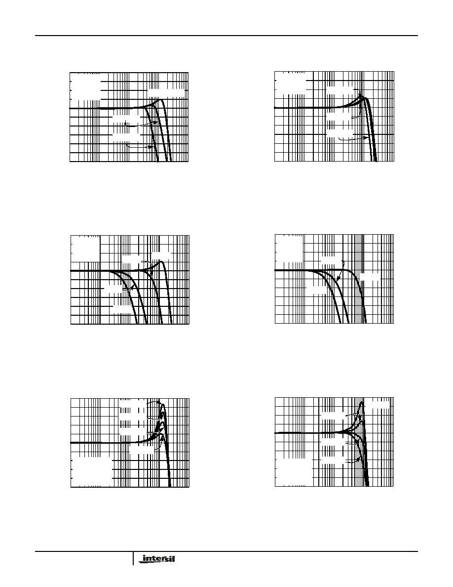
Typical Performance Curves
FIGURE 1. FREQUENCY RESPONSE FOR VARIOUS OUTPUT
VOLTAGE LEVELS
FIGURE 2. SMALL SIGNAL FREQUENCY RESPONSE FOR
VARIOUS R
LOAD
FIGURE 3. SMALL SIGNAL FREQUENCY RESPONSE FOR
VARIOUS NON-INVERTING GAINS
FIGURE 4. SMALL SIGNAL FREQUENCY RESPONSE FOR
VARIOUS INVERTING GAINS
FIGURE 5. SMALL SIGNAL FREQUENCY RESPONSE FOR
VARIOUS C
L
FIGURE 6. SMALL SIGNAL FREQUENCY RESPONSE FOR
VARIOUS C
L
4
2
0
-2
-4
-6
100K
1M
10M
100M
1G
FREQUENCY (Hz)
GAI
N
(
d
B)
V
S
=5V
A
V
=1
R
L
=1k
C
L
=1.5pF
V
OP-P
=200mV
V
OP-P
=1V
V
OP-P
=2V
4
2
0
-2
-4
-6
100K
1M
10M
100M
1G
FREQUENCY (Hz)
GAI
N
(
d
B)
V
S
=5V
A
V
=1
C
L
=1.5pF
R
L
=330
R
L
=1k
R
L
=100
4
2
0
-2
-4
-6
100K
1M
10M
100M
1G
FREQUENCY (Hz)
NORMALIZED GAIN
(dB)
V
S
=5V
R
L
=1k
C
L
=1.5pF
A
V
=1
A
V
=10
A
V
=5
A
V
=2
4
2
0
-2
-4
-6
100K
1M
10M
100M
1G
FREQUENCY (Hz)
NORMALIZED GAIN
(dB)
V
S
=5V
R
L
=1k
C
L
=1.5pF
R
F
=1k
A
V
=-10
A
V
=-2
A
V
=-5
5
3
1
-1
-3
-5
100K
1M
10M
100M
1G
FREQUENCY (Hz)
GAI
N
(
d
B)
V
S
=5V
A
V
=1
R
L
=1k
V
OP-P
=200mV
C
L
=10pF
C
L
=7pF
C
L
=5pF
C
L
=1.5pF
14
10
6
2
-2
-6
100K
1M
10M
100M
1G
FREQUENCY (Hz)
GAI
N
(
d
B)
C
L
=15pF
C
L
=1.5pF
C
L
=56pF
C
L
=35pF
V
S
=5V
A
V
=2
R
L
=1k
R
F
=R
G
=1k
-12
-8
-4
0
4
EL8300
5
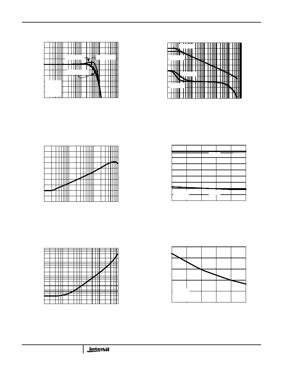
FIGURE 7. SMALL SIGNAL FREQUENCY RESPONSE FOR
VARIOUS R
F
AND R
G
FIGURE 8. OPEN LOOP GAIN AND PHASE vs FREQUENCY
FIGURE 9. COMMON-MODE REJECTION RATIO vs
FREQUENCY
FIGURE 10. SMALL SIGNAL BANDWIDTH vs SUPPLY
VOLTAGE
FIGURE 11. OUTPUT IMPEDANCE vs FREQUENCY
FIGURE 12. SMALL SIGNAL PEAKING vs SUPPLY VOLTAGE
Typical Performance Curves
(Continued)
10
8
6
4
2
0
100K
1M
10M
100M
1G
FREQUENCY (Hz)
GAI
N
(
d
B)
V
S
=5V
A
V
=2
R
L
=1k
C
L
=1.5pF
R
F
=R
G
=2k
R
F
=R
G
=500
R
F
=R
G
=1k
110
70
30
-10
-50
-90
1K
10K
1M
100M
1G
FREQUENCY (Hz)
GAI
N
(
d
B)
R
L
=1k
PHASE (°
)
-45
405
315
225
135
45
100K
10M
R
L
=150
R
L
=150
R
L
=1k
-10
-30
-50
-70
-90
-110
100K
1M
10M
100M
FREQUENCY (Hz)
CMRR
(dB)
230
170
130
210
70
50
3
3.5
4.5
5
5.5
V
S
(V)
BANDWIDTH (
M
Hz
)
R
L
=1k
C
L
=1.5pF
A
V
=1
A
V
=2
190
110
90
150
4
100
10
1
0.1
0.01
10K
100K
1M
10M
FREQUENCY (Hz)
IMPEDANCE (
)
100M
2.5
1
2
0
3
3.5
4.5
5
5.5
V
S
(V)
PEAKING (dB)
A
V
=1
R
L
=1k
C
L
=1.5pF
1.5
0.5
4
EL8300