 | –≠–Ľ–Ķ–ļ—ā—Ä–ĺ–Ĺ–Ĺ—č–Ļ –ļ–ĺ–ľ–Ņ–ĺ–Ĺ–Ķ–Ĺ—ā: EL8403IS | –°–ļ–į—á–į—ā—Ć:  PDF PDF  ZIP ZIP |
1
ģ
FN7106.1
EL8202, EL8203, EL8403
500MHz Rail-to-Rail Amplifiers
The EL8202, EL8203, and EL8403 represent rail-to-rail
amplifiers with a -3dB bandwidth of 500MHz and slew rate of
600V/Ķs. Running off a very low supply current of 5.6mA per
channel, the EL8202, EL8203, and EL8403 also feature
inputs that go to 0.15V below the V
S
- rail. The EL8202 and
EL8203 are dual channel amplifiers. The EL8403 is a quad
channel amplifier.
The EL8202 includes a fast-acting disable/power-down
circuit. With a 25ns disable and a 200ns enable, the EL8202
is ideal for multiplexing applications.
The EL8202, EL8203, and EL8403 are designed for a
number of general purpose video, communication,
instrumentation, and industrial applications. The EL8202 is
available in a 10-pin MSOP package, the EL8203 in 8-pin
SO and 8-pin MSOP packages, and the EL8403 in 14-pin
SO and 16-pin QSOP packages. All are specified for
operation over the -40įC to +85įC temperature range.
Features
∑ 500MHz -3dB bandwidth
∑ 600V/Ķs slew rate
∑ Low supply current = 5.6mA per channel
∑ Supplies from 3V to 5.5V
∑ Rail-to-rail output
∑ Input to 0.15V below V
S
-
∑ Fast 25ns disable (EL8202 only)
∑ Low cost
∑ Pb-Free available (RoHS compliant)
Applications
∑ Video amplifiers
∑ Portable/hand-held products
∑ Communications devices
Ordering Information
PART
NUMBER
PACKAGE
TAPE &
REEL
PKG. DWG. #
EL8202IY
10-Pin MSOP
-
MDP0043
EL8202IY-T7
10-Pin MSOP
7"
MDP0043
EL8202IY-T13
10-Pin MSOP
13"
MDP0043
EL8202IYZ
(See Note)
10-Pin MSOP
(Pb-free)
-
MDP0043
EL8202IYZ-T7
(See Note)
10-Pin MSOP
(Pb-free)
7"
MDP0043
EL8202IYZ-T13
(See Note)
10-Pin MSOP
(Pb-free)
13"
MDP0043
EL8203IS
8-Pin SO
-
MDP0027
EL8203IS-T7
8-Pin SO
7"
MDP0027
EL8203IS-T13
8-Pin SO
13"
MDP0027
EL8203ISZ
(See Note)
8-Pin SO
(Pb-free)
-
MDP0027
EL8203ISZ-T7
(See Note)
8-Pin SO
(Pb-free)
7"
MDP0027
EL8203ISZ-T13
(See Note)
8-Pin SO
(Pb-free)
13"
MDP0027
EL8203IY
8-Pin MSOP
-
MDP0043
EL8203IY-T7
8-Pin MSOP
7"
MDP0043
EL8203IY-T13
8-Pin MSOP
13"
MDP0043
EL8403IS
14-Pin SO
-
MDP0027
EL8403IS-T7
14-Pin SO
7"
MDP0027
EL8403IS-T13
14-Pin SO
13"
MDP0027
EL8403ISZ
(See Note)
14-Pin SO
(Pb-free)
-
MDP0027
EL8403ISZ-T7
(See Note)
14-Pin SO
(Pb-free)
7"
MDP0027
EL8403ISZ-T13
(See Note)
14-Pin SO
(Pb-free)
13"
MDP0027
EL8403IU
16-Pin QSOP
-
MDP0040
EL8403IU-T7
16-Pin QSOP
7"
MDP0040
EL8403IU-T13
16-Pin QSOP
13"
MDP0040
EL8403IUZ
(See Note)
16-Pin QSOP
(Pb-free)
-
MDP0040
EL8403IUZ-T7
(See Note)
16-Pin QSOP
(Pb-free)
7"
MDP0040
EL8403IUZ-T13
(See Note)
16-Pin QSOP
(Pb-free)
13"
MDP0040
NOTE: Intersil Pb-free products employ special Pb-free material sets; molding
compounds/die attach materials and 100% matte tin plate termination finish,
which are RoHS compliant and compatible with both SnPb and Pb-free
soldering operations. Intersil Pb-free products are MSL classified at Pb-free
peak reflow temperatures that meet or exceed the Pb-free requirements of
IPC/JEDEC J STD-020.
Ordering Information
(Continued)
PART
NUMBER
PACKAGE
TAPE &
REEL
PKG. DWG. #
Data Sheet
May 13, 2005
CAUTION: These devices are sensitive to electrostatic discharge; follow proper IC Handling Procedures.
1-888-INTERSIL or 321-724-7143
|
Intersil (and design) is a registered trademark of Intersil Americas Inc.
Copyright © Intersil Americas Inc. 2003. All Rights Reserved. Elantec is a registered trademark of Elantec Semiconductor, Inc.
All other trademarks mentioned are the property of their respective owners.
2
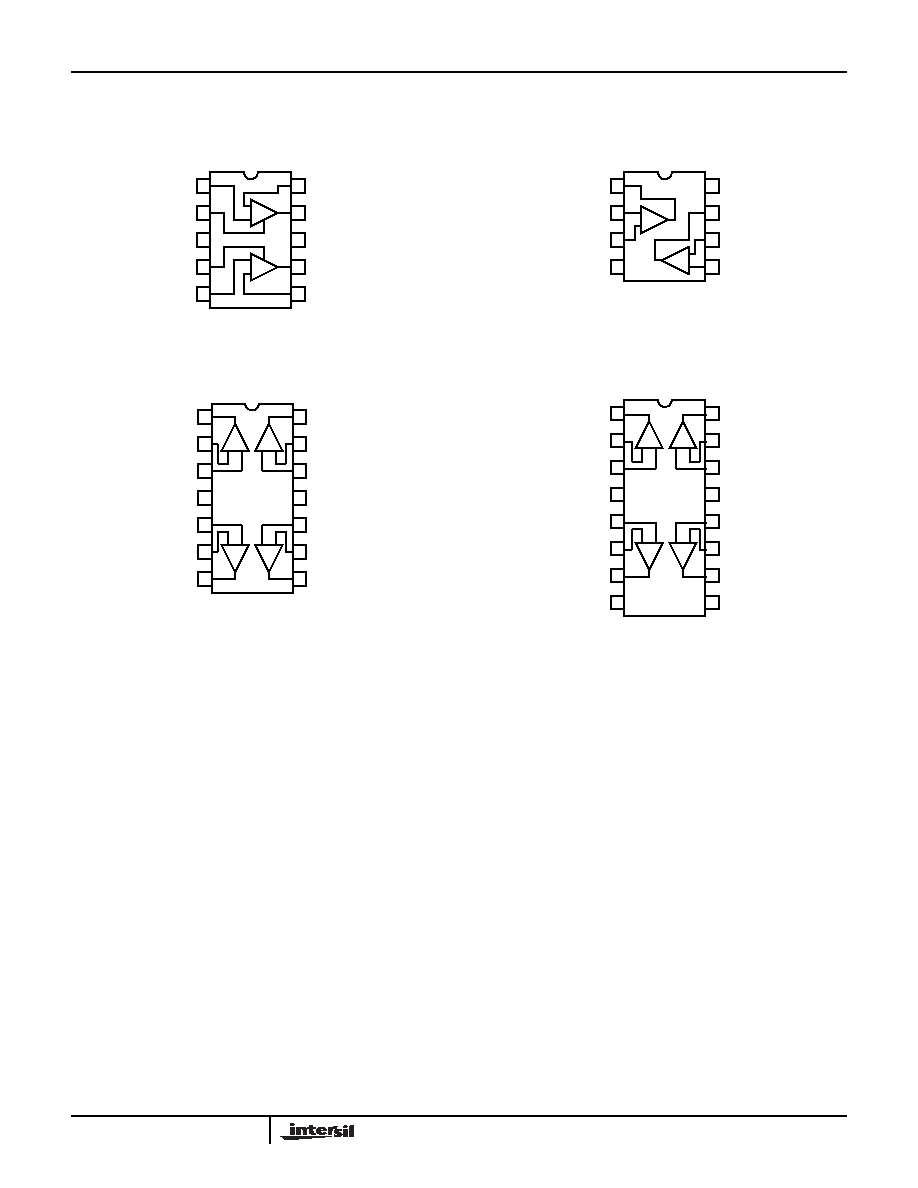
Pinouts
EL8202
(10-PIN MSOP)
TOP VIEW
EL8203
(8-PIN SO, MSOP)
TOP VIEW
EL8403
(14-PIN SO)
TOP VIEW
EL8403
(16-PIN QSOP)
TOP VIEW
-
+
-
+
INA+
CEA
VS-
CEB
INA-
OUTA
VS+
OUTB
INB+
INB-
1
2
3
4
10
9
8
7
5
6
1
2
3
4
8
7
6
5
-
+
-
+
OUTA
INA-
INA+
VS-
VS+
OUTB
INB-
INB+
1
2
3
4
14
13
12
11
5
6
7
10
9
8
OUTA
INA-
INA+
VS+
INB+
INB-
OUTB
OUTD
IND-
IND+
VS-
INC+
INC-
OUTC
- +
-
+
- +
-
+
A
D
B
C
1
2
3
4
16
15
14
13
5
6
7
12
11
10
8
9
OUTA
INA-
INA+
VS+
INB+
INB-
OUTB
OUTD
IND-
IND+
VS-
INC+
INC-
OUTC
NC
NC
- +
-
+
- +
-
+
EL8202, EL8203, EL8403

3
IMPORTANT NOTE: All parameters having Min/Max specifications are guaranteed. Typ values are for information purposes only. Unless otherwise noted, all tests are
at the specified temperature and are pulsed tests, therefore: T
J
= T
C
= T
A
Absolute Maximum Ratings
(T
A
= 25įC)
Supply Voltage from V
S
+ to V
S
- . . . . . . . . . . . . . . . . . . . . . . . . 5.5V
Input Voltage . . . . . . . . . . . . . . . . . . . . . . . . V
S
+ +0.3V to V
S
- -0.3V
Differential Input Voltage . . . . . . . . . . . . . . . . . . . . . . . . . . . . . . . .2V
Continuous Output Current . . . . . . . . . . . . . . . . . . . . . . . . . . . 40mA
Power Dissipation . . . . . . . . . . . . . . . . . . . . . . . . . . . . . See Curves
Storage Temperature . . . . . . . . . . . . . . . . . . . . . . . .-65įC to +150įC
Ambient Operating Temperature . . . . . . . . . . . . . . . .-40įC to +85įC
Operating Junction Temperature . . . . . . . . . . . . . . . . . . . . . . +125įC
CAUTION: Stresses above those listed in "Absolute Maximum Ratings" may cause permanent damage to the device. This is a stress only rating and operation of the
device at these or any other conditions above those indicated in the operational sections of this specification is not implied.
Electrical Specifications
V
S
+
= 5V, V
S
-
= GND, T
A
= 25įC, V
CM
= 2.5V, R
L
to 2.5V, A
V
= 1, Unless Otherwise Specified
PARAMETER
DESCRIPTION
CONDITIONS
MIN
TYP
MAX
UNIT
INPUT CHARACTERISTICS
V
OS
Offset Voltage
-8
-0.8
+8
mV
TCV
OS
Offset Voltage Temperature Coefficient
Measured from T
MIN
to T
MAX
3
ĶV/įC
IB
Input Bias Current
V
IN
= 0V
-9
-6
ĶA
I
OS
Input Offset Current
V
IN
= 0V
0.1
0.6
ĶA
TCI
OS
Input Bias Current Temperature
Coefficient
Measured from T
MIN
to T
MAX
2
nA/įC
CMRR
Common Mode Rejection Ratio
V
CM
= -0.15V to +3.5V (EL8202,EL8203)
70
95
dB
V
CM
= -0.15V to +3.5V (EL8403)
60
85
dB
CMIR
Common Mode Input Range
V
S
- -
0.15
V
S
+ -
1.5
V
R
IN
Input Resistance
Common Mode
3.5
M
C
IN
Input Capacitance
0.5
pF
AVOL
Open Loop Gain
V
OUT
= +1.5V to +3.5V, R
L
= 1k
to GND
75
90
dB
V
OUT
= +1.5V to +3.5V, R
L
= 150
to GND
80
dB
OUTPUT CHARACTERISTICS
R
OUT
Output Resistance
A
V
= +1
30
m
V
OP
Positive Output Voltage Swing
R
L
= 1k
4.85
4.9
V
R
L
= 150
4.6
4.7
V
V
ON
Negative Output Voltage Swing
R
L
= 150
100
150
mV
R
L
= 1k
(EL8202,EL8203)
25
50
mV
R
L
= 1k
(EL8403)
50
100
mV
I
OUT
Linear Output Current
65
mA
I
SC
(source)
Short Circuit Current
R
L
= 10
60
80
mA
I
SC
(sink)
Short Circuit Current
R
L
= 10
120
150
mA
POWER SUPPLY
PSRR
Power Supply Rejection Ratio
V
S
+ = 4.5V to 5.5V
70
95
dB
I
S-ON
Supply Current - Enabled (per amplifier)
5.6
6.2
mA
I
S-OFF
Supply Current - Disabled (per amplifier)
40
90
ĶA
ENABLE (EL8202 ONLY)
t
EN
Enable Time
200
ns
t
DS
Disable Time
25
ns
V
IH-ENB
ENABLE Pin Voltage for Power-up
0.8
V
V
IL-ENB
ENABLE Pin Voltage for Shut-down
2
V
EL8202, EL8203, EL8403
4
I
IH-ENB
ENABLE Pin Input Current High
8.6
ĶA
I
IL-ENB
ENABLE Pin Input for Current Low
0.01
ĶA
AC PERFORMANCE
BW
-3dB Bandwidth
A
V
= +1, R
F
= 0
, C
L
= 2.5pF
500
MHz
A
V
= -1, R
F
= 1k
, C
L
= 2.5pF
140
MHz
A
V
= +2, R
F
= 1k
, C
L
= 2.5pF
165
MHz
A
V
= +10, R
F
= 1k
, C
L
= 2.5pF
18
MHz
BW
Ī0.1dB Bandwidth
A
V
= +1, R
F
= 0
, C
L
= 2.5pF
35
MHz
Peak
Peaking
A
V
= +1, R
L
= 1k
, C
L
= 2.5pF
2
dB
GBWP
Gain Bandwidth Product
200
MHz
PM
Phase Margin
R
L
= 1k
, C
L
= 2.5pF
55
į
SR
Slew Rate
A
V
= 2, R
L
= 100
, V
OUT
= 0.5V to 4.5V
500
600
V/Ķs
t
R
Rise Time
2.5V
STEP
, 20% - 80%
4
ns
t
F
Fall Time
2.5V
STEP
, 20% - 80%
2
ns
OS
Overshoot
200mV step
10
%
t
PD
Propagation Delay
200mV step
1
ns
t
S
0.1% Settling Time
200mV step
15
ns
dG
Differential Gain
A
V
= +2, R
F
= 1k
, R
L
= 150
0.01
%
dP
Differential Phase
A
V
= +2, R
F
= 1k
, R
L
= 150
0.01
į
e
N
Input Noise Voltage
f = 10kHz
12
nV/
Hz
i
N
+
Positive Input Noise Current
f = 10kHz
1.7
pA/
Hz
i
N
-
Negative Input Noise Current
f = 10kHz
1.3
pA/
Hz
e
S
Channel Separation
f = 100kHz
95
dB
Electrical Specifications
V
S
+
= 5V, V
S
-
= GND, T
A
= 25įC, V
CM
= 2.5V, R
L
to 2.5V, A
V
= 1, Unless Otherwise Specified (Continued)
PARAMETER
DESCRIPTION
CONDITIONS
MIN
TYP
MAX
UNIT
Pin Descriptions
EL8202
(MSOP-10)
EL8203
(SO-8,
MSOP-8)
EL8403
(SO-14)
EL8403
(QSOP-16)
NAME
FUNCTION
1, 5
3, 5
3, 5, 10, 12
3,5,12,14
IN+
Non-inverting input for each channel
2, 4
CE
Enable and disable input for each channel
3
4
11
13
VS-
Negative power supply
6, 10
2, 6
2, 6, 9, 13
2,6,11,15
IN-
Inverting input for each channel
7, 9
1, 7
1, 7, 8, 14
1,7,10,16
OUT
Amplifier output for each channel
8
8
4
4
VS+
Positive power supply
EL8202, EL8203, EL8403
5
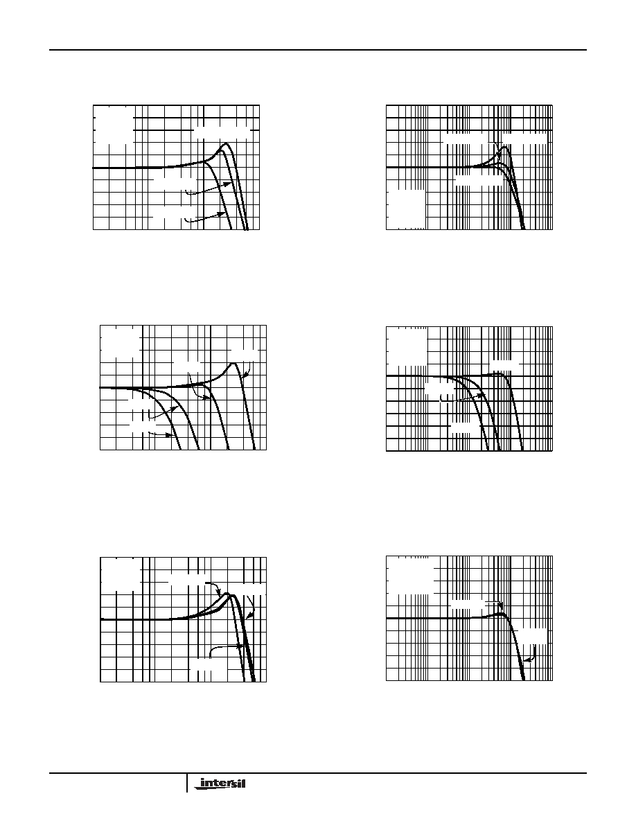
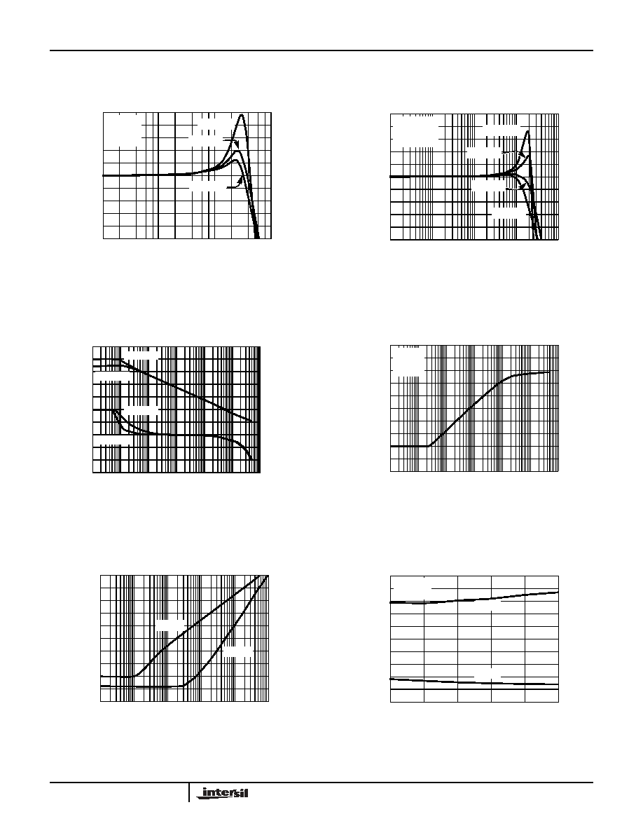
Typical Performance Curves
FIGURE 1. FREQUENCY RESPONSE FOR VARIOUS OUTPUT
VOLTAGE LEVELS
FIGURE 2. SMALL SIGNAL FREQUENCY RESPONSE
vs R
F
AND R
G
FIGURE 3. SMALL SIGNAL FREQUENCY RESPONSE FOR
VARIOUS NON-INVERTING GAINS
FIGURE 4. SMALL SIGNAL FREQUENCY RESPONSE FOR
VARIOUS INVERTING GAINS
FIGURE 5. SMALL SIGNAL FREQUENCY RESPONSE FOR
VARIOUS NON-INVERTING GAINS
FIGURE 6. SMALL SIGNAL FREQUENCY RESPONSE vs
VARIOUS R
LOAD
5
3
1
-1
-3
-5
1M
10M
100M
1G
FREQUENCY (Hz)
GAI
N
(
d
B)
V
S
=5V
A
V
=1
R
L
=1k
C
L
=2.5pF
4
2
0
-2
-4
V
OP-P
=200mV
V
OP-P
=1V
V
OP-P
=2V
5
3
1
-1
-3
-5
100K
1M
10M
100M
1G
FREQUENCY (Hz)
NORMALIZED GAIN
(
d
B)
V
S
=5V
A
V
=2
R
L
=1k
C
L
=2.5pF
R
F
=R
G
=2k
R
F
=R
G
=500
R
F
=R
G
=1k
5
3
1
-1
-3
-5
1M
10M
100M
1G
FREQUENCY (Hz)
NORMALIZED GAIN
(
d
B)
A
V
=10
A
V
=1
V
S
=5V
C
L
=2.5pF
R
L
=1k
A
V
=5
A
V
=2
4
2
0
-2
-4
4
2
0
-2
-4
-6
100K
1M
10M
100M
1G
FREQUENCY (Hz)
NORMALIZED GAIN
(dB)
A
V
=-10
V
S
=5V
C
L
=2.5pF
R
L
=1k
R
F
=1k
A
V
=-1
A
V
=-5
5
3
1
-1
-3
-5
1M
10M
100M
1G
FREQUENCY (Hz)
GAI
N
(
d
B)
R
L
=1k
V
S
=5V
A
V
=1
C
L
=2.5pF
4
2
0
-2
-4
R
L
=100
R
L
=500
11
9
7
5
3
1
100K
1M
10M
100M
1G
FREQUENCY (Hz)
GAI
N
(
d
B)
V
S
=5V
A
V
=2
C
L
=2.5pF
R
F
=R
G
=1k
R
L
=500
R
L
=1k
,
150
EL8202, EL8203, EL8403
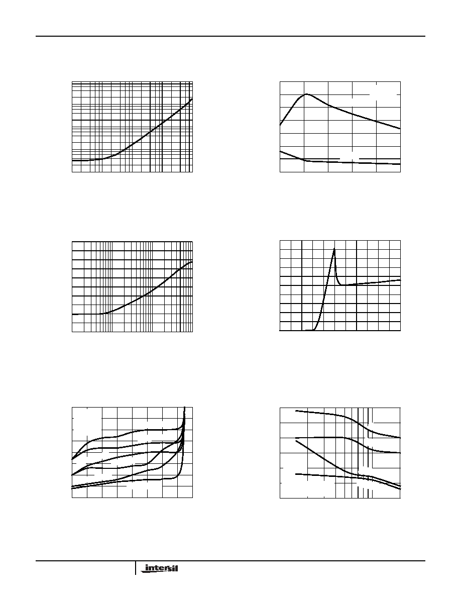
6
FIGURE 7. SMALL SIGNAL FREQUENCY RESPONSE vs C
L
FIGURE 8. SMALL SIGNAL FREQUENCY RESPONSE FOR
VARIOUS C
L
FIGURE 9. OPEN LOOP GAIN AND PHASE vs FREQUENCY
FIGURE 10. DISABLED OUTPUT ISOLATION FREQUENCY
RESPONSE
FIGURE 11. POWER SUPPLY REJECTION
RATIO vs FREQUENCY
FIGURE 12. SMALL SIGNAL BANDWIDTH vs
SUPPLY VOLTAGE
Typical Performance Curves
(Continued)
5
3
1
-1
-3
-5
1M
10M
100M
1G
FREQUENCY (Hz)
GAI
N
(
d
B)
C
L
=5.4pF
C
L
=1.5pF
V
S
=5V
A
V
=1
R
L
=1k
4
3
0
-2
-4
C
L
=2.5pF
16
12
8
4
0
-4
100K
1M
10M
100M
1G
FREQUENCY (Hz)
G
A
IN (
d
B
)
V
S
=5V
A
V
=2
R
F
=R
G
=1k
C
L
=28.5pF
C
L
=2.5pF
14
10
6
2
-2
C
L
=10pF
C
L
=20pF
110
70
30
-10
-50
-90
1K
10K
1M
100M
1G
FREQUENCY (Hz)
GAI
N
(d
B)
R
L
=1k
PHASE (į
)
-45
405
315
225
135
45
100K
10M
R
L
=150
R
L
=150
R
L
=1k
-10
-30
-50
-70
-90
-110
1K
10K
100K
100M
1G
FREQUENCY (Hz)
GAI
N
(
d
B)
V
S
=5V
A
V
=1
R
L
=1k
1M
10M
-10
-30
-50
-70
-90
-110
1K
10K
10M
100M
FREQUENCY (Hz)
P
S
RR (
d
B
)
100K
1M
PSRR-
PSRR+
600
400
350
550
200
150
3
3.5
4.5
5
5.5
VS (V)
BANDWIDTH (MHz)
A
V
=1
500
300
250
4
R
L
=1k
C
L
=2.5pF
A
V
=2
450
100
EL8202, EL8203, EL8403
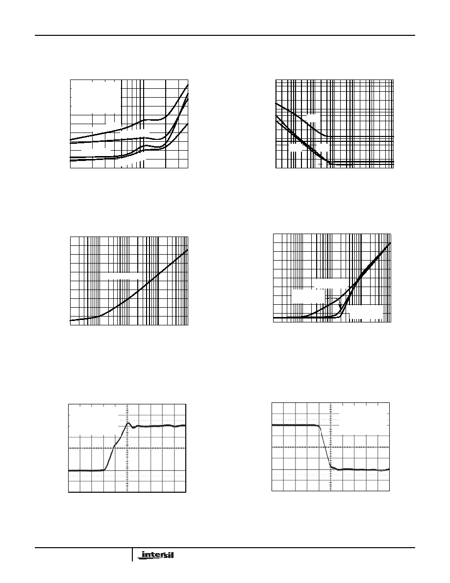
7
FIGURE 13. OUPUT IMPEDANCE vs FREQUENCY
FIGURE 14. SMALL SIGNAL PEAKING vs SUPPLY VOLTAGE
FIGURE 15. COMMON-MODE REJECTION RATIO vs
FREQUENCY
FIGURE 16. SUPPLY CURRENT vs SUPPLY VOLTAGE
(PER CHANNEL)
FIGURE 17. HARMONIC DISTORTION vs OUTPUT VOLTAGE
FIGURE 18. HARMONIC DISTORTION vs LOAD RESISTANCE
Typical Performance Curves
(Continued)
100
10
1
0.1
0.01
10K
100K
1M
10M
FREQUENCY (Hz)
IMPEDANCE (
)
100M
3.5
2
1.5
3
0
3
3.5
4.5
5
5.5
VS (V)
PE
AK
ING (dB)
R
L
=1k
C
L
=1.5pF
A
V
=1
A
V
=2
2.5
1
0.5
4
-15
-35
-55
-75
-95
-115
100K
1M
10M
100M
FREQUENCY (Hz)
CMRR (
d
B)
10
4
8
0
0
1
3
4
5.5
V
S
(V)
I
S
(mA)
6
2
2
0.5
1.5
3.5
4.5 5
2.5
-60
-70
-80
-100
1
5
V
OP-P
(V)
D
I
S
T
ORT
I
O
N
(
d
Bc
)
V
S
=5V
R
L
=1k
C
L
=2.5pF
A
V
=2
-90
3
4
2
HD2@10MHz
HD2@5MHz
HD2
@1M
Hz
HD3@10MH
z
HD3@5
MHz
HD3@1MHz
-70
-75
-90
-100
100
2K
R
LOAD
(
)
DIS
T
ORTION (
d
Bc
)
-95
1K
V
O
=1V
P-P
for A
V
=1
V
O
=2V
P-P
for A
V
=2
-85
-80
HD2@A
V
=2
HD2@A
V
=1
HD3@A
V
=2
HD3@A
V
=1
V
S
=5V
f=5MHz
EL8202, EL8203, EL8403
8
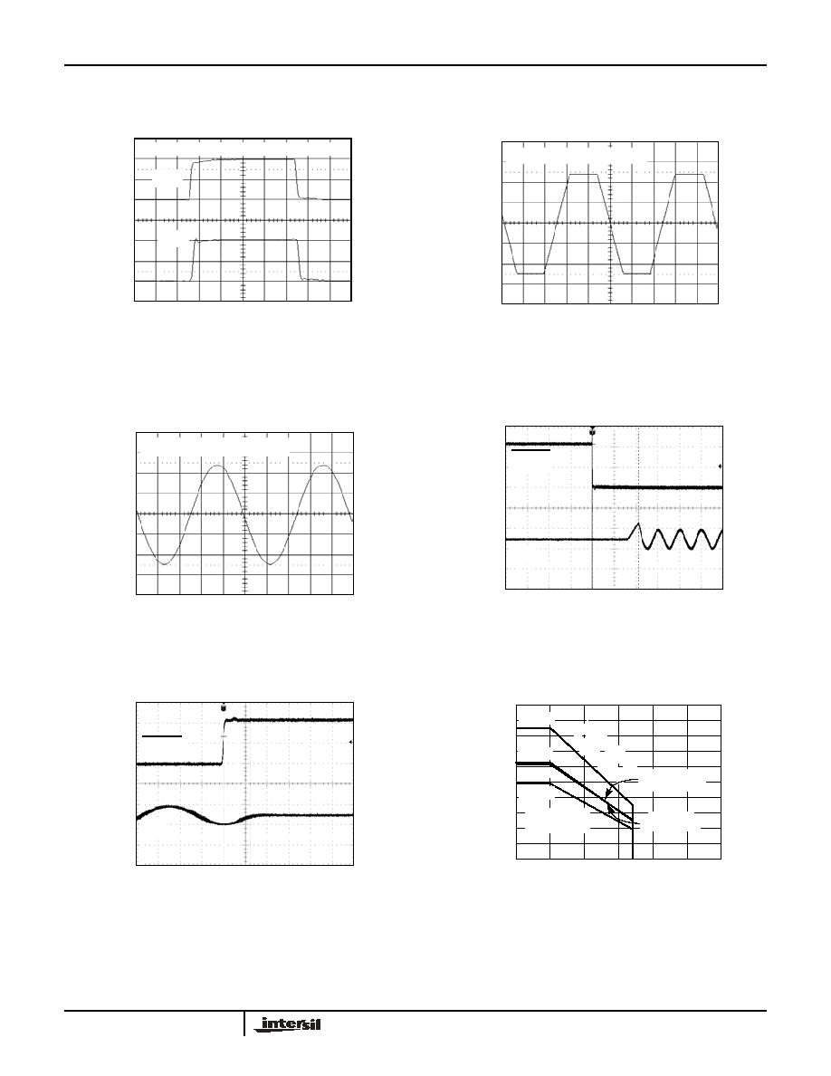
FIGURE 19. HARMONIC DISTORTION vs FREQUENCY
FIGURE 20. VOLTAGE AND CURRENT NOISE vs FREQUENCY
FIGURE 21. CHANNEL SEPARATION vs FREQUENCY (EL8202
AND EL8203)
FIGURE 22. CHANNEL SEPARATION vs FREQUENCY
(EL8403)
FIGURE 23. LARGE SIGNAL TRANSIENT
RESPONSE - RISING
FIGURE 24. LARGE SIGNAL TRANSIENT
RESPONSE - FALLING
Typical Performance Curves
(Continued)
-50
-70
-90
-60
-100
1
40
FREQUENCY (MHz)
DIST
ORTION (dBc)
V
S
=5V
R
L
=1k
C
L
=2.5pF
V
O
=1V
P-P
for A
V
=1
V
O
=2V
P-P
for A
V
=2
10
HD2@A
V
=2
-80
HD2@A
V
=1
HD3@A
V
=2
HD3@
A
V
=1
1K
100
1
10
100
10K
100K
10M
FREQUENCY (Hz)
VO
L
T
AGE NOI
SE (nV/
Hz)
CURRENT N
O
IS
E (pA/
Hz),
e
N
10
1K
1M
I
N
+
I
N
-
0
-20
-40
-60
-80
-100
100K
1M
10M
100M
1G
FREQUENCY (Hz)
CHANNEL S
E
P
ARA
TION
(dB)
CH1<=>CH2
-10
-30
-50
-70
-90
0
-20
-40
-60
-80
-100
100K
1M
10M
100M
1G
FREQUENCY (Hz)
CHA
NNE
L
SE
P
A
RA
TION
(dB)
-10
-30
-50
-70
-90
CH1<=>CH3
CH2<=>CH4
CH1<=>CH2
CH1<=>CH4
CH2<=>CH3
2ns/DIV
1.5
2.5
3.5
V
S
=5V
A
V
=1
R
L
=1k
to 2.5V
C
L
=5pF
2ns/DIV
1.5
2.5
3.5
V
S
=5V
A
V
=1
R
L
=1k
to 2.5V
C
L
=5pF
EL8202, EL8203, EL8403
9
FIGURE 25. SMALL SIGNAL TRANSIENT REPONSE
FIGURE 26. OUTPUT SWING
FIGURE 27. OUTPUT SWING
FIGURE 28. ENABLED RESPONSES (EL8202)
FIGURE 29. DISABLED RESPONSE (EL8202)
FIGURE 30. PACKAGE POWER DISSIPATION vs AMBIENT
TEMPERATURE
Typical Performance Curves
(Continued)
10ns/DIV
2.4
2.6
2.5
2.6
2.4
2.5
V
OUT
V
IN
V
S
=5V, A
V
=1, R
L
=1k
TO 2.5V, C
L
= 2.5pF
2Ķs/DIV
0
2.5
5
V
S
=5V, A
V
=5, R
L
=1k
to 2.5V
2Ķs/DIV
0
2.5
5
V
S
=5V, A
V
=5, R
L
=1k
TO 2.5V
CH1, CH2, 1V/DIV, M=100ns
CH2
CH1
ENABLE
INPUT
V
OUT
CH1, CH2, 0.5V/DIV, M=20ns
CH2
CH1
ENABLE
INPUT
V
OUT
486mW
JA
=206įC/W
MSOP8/10
625mW
1
0.9
0.8
0.6
0.4
0.1
0
0
25
50
75
100
150
AMBIENT TEMPERATURE (įC)
PO
WER D
I
SS
IP
A
T
I
O
N (W)
125
85
JEDEC JESD51-3 LOW EFFECTIVE THERMAL
CONDUCTIVITY TEST BOARD
0.2
0.7
0.3
0.5
833mW
JA
=12
0įC
/W
SO
14
633mW
JA
=158įC/W
JA
=160įC/W
SO8
QSOP16
EL8202, EL8203, EL8403
10
Simplified Schematic Diagram
Description of Operation and Application
Information
Product Description
The EL8202, EL8203 and EL8403 are wide bandwidth,
single supply, low power and rail-to-rail output voltage
feedback operational amplifiers. The amplifiers are internally
compensated for closed loop gain of +1 of greater.
Connected in voltage follower mode and driving a 1k
load,
the EL8202, EL8203 and EL8403 have a -3dB bandwidth of
500MHz. Driving a 150
load, the bandwidth is about
350MHz while maintaining a 600V/us slew rate. The EL8202
is available with a power down pin to reduce power to 30ĶA
typically while the amplifier is disabled.
Input, Output and Supply Voltage Range
The EL8202, EL8203 and EL8403 have been designed to
operate with a single supply voltage from 3V to 5.0V. Split
supplies can also be used as long as their total voltage is
within 3V to 5.0V. The amplifiers have an input common
mode voltage range from 0.15V below the negative supply
(V
S
- pin) to within 1.5V of the positive supply (V
S
+ pin). If the
input signal is outside the above specified range, it will cause
the output signal to be distorted.
The output of the EL8202, EL8203 and EL8403 can swing
rail to rail. As the load resistance becomes lower, the ability
to drive close to each rail is reduced. For the load resistor
1k
, the output swing is about 4.9V at a 5V supply. For the
load resistor 150
, the output swing is about 4.6V.
FIGURE 31. PACKAGE POWER DISSIPATION vs AMBIENT TEMPERATURE
Typical Performance Curves
(Continued)
909mW
1.4
1.2
1
0.8
0.6
0.2
0
0
25
50
75
100
150
AMBIENT TEMPERATURE (įC)
P
O
WER DI
SSI
PATIO
N
(
W
)
125
85
JEDEC JESD51-7 HIGH EFFECTIVE
THERMAL CONDUCTIVITY TEST BOARD
0.4
JA
=88
įC
/W
SO
14
JA
=110įC/W
SO8
893mW
870mW
JA
=115įC/W
MSOP8/10
JA
=112įC/W
QSOP16
1.136W
IN+
IN-
I
1
I
2
R
6
R
3
R
1
R
2
Q
1
Q
2
R
7
V
BIAS1
Q
5
Q
6
R
8
Q
7
Q
8
R
9
Q
3
Q
4
R
4
R
5
V
S-
OUT
V
BIAS2
V
S+
DIFFERENTIAL TO
DRIVE
GENERATOR
SINGLE ENDED
EL8202, EL8203, EL8403
11
Choice of Feedback Resistor and Gain Bandwidth
Product
For applications that require a gain of +1, no feedback
resistor is required. Just short the output pin to the inverting
input pin. For gains greater than +1, the feedback resistor
forms a pole with the parasitic capacitance at the inverting
input. As this pole becomes smaller, the amplifier's phase
margin is reduced. This causes ringing in the time domain
and peaking in the frequency domain. Therefore, R
F
has
some maximum value that should not be exceeded for
optimum performance. If a large value of R
F
must be used, a
small capacitor in the few pF range in parallel with R
F
can
help to reduce the ringing and peaking at the expense of
reducing the bandwidth.
As far as the output stage of the amplifier is concerned, the
output stage is also a gain stage with the load. R
F
and R
G
appear in parallel with R
L
for gains other than +1. As this
combination gets smaller, the bandwidth falls off.
Consequently, R
F
also has a minimum value that should not
be exceeded for optimum performance. For gain of +1, R
F
=0
is optimum. For the gains other than +1, optimum response
is obtained with R
F
between 300
to 1k.
The EL8202, EL8203 and EL8403 have a gain bandwidth
product of 200MHz. For gains
5, its bandwidth can be
predicted by the following equation:
Video Performance
For good video performance, an amplifier is required to
maintain the same output impedance and the same
frequency response as DC levels are changed at the output.
This is especially difficult when driving a standard video load
of 150
, because the change in output current with DC level.
Special circuitry has been incorporated in the EL8202,
EL8203 and EL8403 to reduce the variation of the output
impedance with the current output. This results in dG and dP
specifications of 0.01% and 0.01
į, while driving 150 at a
gain of 2. Driving high impedance loads would give a similar
or better dG and dP performance.
Driving Capacitive Loads and Cables
The EL8202, EL8203 and EL8403 can drive 5pF loads in
parallel with 1k
with less than 5dB of peaking at gain of +1.
If less peaking is desired in applications, a small series
resistor (usually between 5
to 50) can be placed in series
with the output to eliminate most peaking. However, this will
reduce the gain slightly. If the gain setting is greater than 1,
the gain resistor R
G
can then be chosen to make up for any
gain loss which may be created by the additional series
resistor at the output.
When used as a cable driver, double termination is always
recommended for reflection-free performance. For those
applications, a back-termination series resistor at the
amplifier's output will isolate the amplifier from the cable and
allow extensive capacitive drive. However, other applications
may have high capacitive loads without a back-termination
resistor. Again, a small series resistor at the output can help
to reduce peaking.
Disable/Power-Down
The EL8202 can be disabled and placed its output in a high
impedance state. The turn off time is about 25ns and the turn
on time is about 200ns. When disabled, the amplifier's
supply current is reduced to 40ĶA typically, thereby
effectively eliminating the power consumption. The
amplifier's power down can be controlled by standard TTL or
CMOS signal levels at the ENABLE pin. The applied logic
signal is relative to V
S
- pin. Letting the ENABLE pin float or
applying a signal that is less than 0.8V above V
S
- will enable
the amplifier. The amplifier will be disabled when the signal
at ENABLE pin is 2V above V
S
-.
Output Drive Capability
The EL8202, EL8203 and EL8403 do not have internal short
circuit protection circuitry. They have a typical short circuit
current of 80mA sourcing and 150mA sinking for the output
is connected to half way between the rails with a 10
resistor. If the output is shorted indefinitely, the power
dissipation could easily increase such that the part will be
destroyed. Maximum reliability is maintained if the output
current never exceeds Ī40mA. This limit is set by the design
of the internal metal interconnections.
Power Dissipation
With the high output drive capability of the EL8202, EL8203
and EL8403. It is possible to exceed the 125
įC absolute
maximum junction temperature under certain load current
conditions. Therefore, it is important to calculate the
maximum junction temperature for the application to
determine if the load conditions or package types need to be
modified for the amplifier to remain in the safe operating
area.
The maximum power dissipation allowed in a package is
determined according to:
Where:
T
JMAX
= Maximum junction temperature
T
AMAX
= Maximum ambient temperature
JA
= Thermal resistance of the package
The maximum power dissipation actually produced by an IC
is the total quiescent supply current times the total power
supply voltage, plus the power in the IC due to the load, or:
For sourcing:
Gain BW
◊
200MHz
=
PD
MAX
T
JMAX
T
AMAX
≠
JA
---------------------------------------------
=
EL8202, EL8203, EL8403
12
For sinking:
Where:
V
S
= Total supply voltage
I
SMAX
= Maximum quiescent supply current
V
OUTi
= Maximum output voltage of the application for
each channel
R
LOADi
= Load resistance tied to ground for each
channel
I
LOADi
= Load current for each channel
By setting the two PD
MAX
equations equal to each other, we
can solve the output current and R
LOADi
to avoid the device
overheat.
Power Supply Bypassing and Printed Circuit
Board Layout
As with any high frequency device, a good printed circuit
board layout is necessary for optimum performance. Lead
lengths should be as short as possible. The power supply
pin must be well bypassed to reduce the risk of oscillation.
For normal single supply operation, where the V
S
- pin is
connected to the ground plane, a single 4.7ĶF tantalum
capacitor in parallel with a 0.1ĶF ceramic capacitor from V
S
+
to GND will suffice. This same capacitor combination should
be placed at each supply pin to ground if split supplies are to
be used. In this case, the V
S
- pin becomes the negative
supply rail.
For good AC performance, parasitic capacitance should be
kept to a minimum. Use of wire wound resistors should be
avoided because of their additional series inductance. Use
of sockets should also be avoided if possible. Sockets add
parasitic inductance and capacitance that can result in
compromised performance. Minimizing parasitic capacitance
at the amplifier's inverting input pin is very important. The
feedback resistor should be placed very close to the
inverting input pin. Strip line design techniques are
recommended for the signal traces.
Typical Applications
VIDEO SYNC PULSE REMOVER
Many CMOS analog to digital converters have a parasitic
latch up problem when subjected to negative input voltage
levels. Since the sync tip contains no useful video
information and it is a negative going pulse, we can chop it
off. Figure 32 shows a gain of 2 connections. Figure 33
shows the complete input video signal applied at the input,
as well as the output signal with the negative going sync
pulse removed.
MULTIPLEXER
Besides the normal power down usage, the ENABLE pin of
the EL8202 can be used for multiplexing applications. Figure
34 shows two EL8202 with the outputs tied together, driving
a back terminated 75
video load. A 2V
P-P
2MHz sine wave
is applied to Amp A and a 1V
P-P
2MHz sine wave is applied
to Amp B. Figure 33 shows the ENABLE signal and the
resulting output waveform at V
OUT
. Observe the break-
before-make operation of the multiplexing. Amp A is on and
V
IN1
is passed through to the output when the ENABLE
signal is low and turns off in about 25ns when the ENABLE
signal is high. About 200ns later, Amp B turns on and V
IN2
is
passed through to the output. The break-before-make
operation ensures that more than one amplifier isn't trying to
drive the bus at the same time.
PD
MAX
V
S
I
SMAX
V
S
V
OUTi
≠
(
)
V
OUTi
R
Li
-----------------
◊
+
◊
=
PD
MAX
V
S
I
SMAX
V
OUTi
V
S
-
≠
(
) I
LOADi
◊
+
◊
=
FIGURE 32. SYNC PULSE REMOVER
5V
1K
V
OUT
V
IN
75
+
-
75
1K
75
V
S+
V
S-
FIGURE 33. VIDEO SIGNAL
1V
0.5V
0V
1V
0.5V
0V
M = 10Ķs/DIV
V
OUT
V
IN
EL8202, EL8203, EL8403
13
SINGLE SUPPLY VIDEO LINE DRIVER
The EL8202, EL8203 and EL8403 are wideband rail-to-rail
output op amplifiers with large output current, excellent dG,
dP, and low distortion that allow them to drive video signals
in low supply applications. Figure 36 is the single supply
non-inverting video line driver configuration and Figure 37 is
the inverting video ling driver configuration. The signal is AC
coupled by C
1
. R
1
and R
2
are used to level shift the input
and output to provide the largest output swing. R
F
and R
G
set the AC gain. C
2
isolates the virtual ground potential. R
T
and R
3
are the termination resistors for the line. C
1
, C
2
and
C
3
are selected big enough to minimize the droop of the
luminance signal.
FIGURE 34. TWO TO ONE MULTIPLEXER
+2.5V
1K
2MHz
75
+
-
1K
75
-2.5V
V
OUT
75
1V
P-P
B
+2.5V
1K
2MHz
+
-
1K
75
-2.5V
2V
P-P
A
ENABLE
FIGURE 35.
0V
-0.5V
-1.5V
-2.5V
1V
0V
M = 50ns/DIV
A
ENABLE
B
-1V
FIGURE 36. 5V SINGLE SUPPLY NON INVERTING
VIDEO LINE DRIVER
FIGURE 37. SINGLE SUPPLY INVERTING VIDEO LINE DRIVER
FIGURE 38. VIDEO LINE DRIVER FREQUENCY RESPONSE
5V
R
F
V
OUT
V
IN
75
+
-
75
1k
75
C
3
470ĶF
R
3
C
1
47ĶF
R
T
10K
10K
R
2
R
1
1k
R
G
C
2
220ĶF
5V
R
F
V
OUT
V
IN
75
-
+
75
500
75
C
3
470ĶF
R
3
C
1
47ĶF
R
T
10K
10K
R
2
R
1
1k
R
G
C
2
220ĶF
5V
4
3
2
1
0
-1
-2
-3
-4
-5
-6
NORMALIZE
D
GAIN
(
d
B
)
100K
1M
10M
100M 500M
FREQUENCY (Hz)
A
V
= -2
A
V
= 2
EL8202, EL8203, EL8403

14
SO Package Outline Drawing
EL8202, EL8203, EL8403
15
MSOP Package Outline Drawing
EL8202, EL8203, EL8403
16
All Intersil U.S. products are manufactured, assembled and tested utilizing ISO9000 quality systems.
Intersil Corporation's quality certifications can be viewed at www.intersil.com/design/quality
Intersil products are sold by description only. Intersil Corporation reserves the right to make changes in circuit design, software and/or specifications at any time without
notice. Accordingly, the reader is cautioned to verify that data sheets are current before placing orders. Information furnished by Intersil is believed to be accurate and
reliable. However, no responsibility is assumed by Intersil or its subsidiaries for its use; nor for any infringements of patents or other rights of third parties which may result
from its use. No license is granted by implication or otherwise under any patent or patent rights of Intersil or its subsidiaries.
For information regarding Intersil Corporation and its products, see www.intersil.com
QSOP Package Outline Drawing
NOTE: The package drawing shown here may not be the latest version. To check the latest revision, please refer to the Intersil website at
http://www.intersil.com/design/packages/index.asp
EL8202, EL8203, EL8403