 | –≠–ª–µ–∫—Ç—Ä–æ–Ω–Ω—ã–π –∫–æ–º–ø–æ–Ω–µ–Ω—Ç: EL9110IU | –°–∫–∞—á–∞—Ç—å:  PDF PDF  ZIP ZIP |
1
Æ
FN7305.4
EL9110
Differential Receiver/Equalizer
The EL9110 is a single channel differential receiver and
equalizer. It contains a high speed differential receiver with 5
programmable poles. The outputs of these pole blocks are
then summed into an output buffer. The equalization length
is set with the voltage on a single pin. The EL9110 also
contains a three-statable output, enabling multiple devices to
be connected in parallel and used in a multiplexing
application.
The gain can be adjusted up or down by 6dB using the
V
GAIN
control signal. In addition, a further 6dB of gain can
be switched in to provide a matched drive into a cable.
The EL9110 has a bandwidth of 150MHz and consumes just
33mA on ±5V supply. A single input voltage is used to set the
compensation levels for the required length of cable.
The EL9110 is available in the 16-pin QSOP package and is
specified for operation over the full -40∞C to +85∞C
temperature range.
Features
∑ 150MHz -3dB bandwidth
∑ CAT-5 compensation
- 75MHz @ 1000 ft
- 125MHz @ 500 ft
∑ 33mA supply current
∑ Differential input range 3.2V
∑ Common mode input range ±4.5V
∑ ±5V supply
∑ Output to within 1.5V of supplies
∑ Available in 16-pin QSOP package
∑ Pb-Free plus anneal available (RoHS compliant)
Applications
∑ Twisted-pair receiving/equalizer
∑ KVM (Keyboard/Video/Mouse)
∑ VGA over twisted-pair
∑ Security video
Pinout
EL9110
(16-PIN QSOP)
TOP VIEW
Ordering Information
PART
NUMBER
PACKAGE
TAPE & REEL
PKG. DWG. #
EL9110IU
16-Pin QSOP
-
MDP0040
EL9110IU-T7
16-Pin QSOP
7"
MDP0040
EL9110IU-T13
16-Pin QSOP
13"
MDP0040
EL9110IUZ
(See Note)
16-Pin QSOP
(Pb-free)
-
MDP0040
EL9110IUZ-T7
(See Note)
16-Pin QSOP
(Pb-free)
7"
MDP0040
EL9110IUZ-T13
(See Note)
16-Pin QSOP
(Pb-free)
13"
MDP0040
NOTE: Intersil Pb-free plus anneal products employ special Pb-free
material sets; molding compounds/die attach materials and 100%
matte tin plate termination finish, which are RoHS compliant and
compatible with both SnPb and Pb-free soldering operations. Intersil
Pb-free products are MSL classified at Pb-free peak reflow
temperatures that meet or exceed the Pb-free requirements of
IPC/JEDEC J STD-020.
1
2
3
4
16
15
14
13
5
6
7
12
11
10
8
9
CTRL_REF
VCTRL
VINP
VINM
VS-
CMOUT
VGAIN
LOGIC_REF
CMEXT
VS+
ENBL
VSA+
VOUT
VSA-
0V
X2
Data Sheet
July 15, 2005
CAUTION: These devices are sensitive to electrostatic discharge; follow proper IC Handling Procedures.
1-888-INTERSIL or 1-888-468-3774
|
Intersil (and design) is a registered trademark of Intersil Americas Inc.
Copyright Intersil Americas Inc. 2003, 2005. All Rights Reserved
All other trademarks mentioned are the property of their respective owners.
2
IMPORTANT NOTE: All parameters having Min/Max specifications are guaranteed. Typ values are for information purposes only. Unless otherwise noted, all tests are
at the specified temperature and are pulsed tests, therefore: T
J
= T
C
= T
A
Absolute Maximum Ratings
(T
A
= 25∞C)
Supply Voltage between V
S
+ and V
S
- . . . . . . . . . . . . . . . . . . . . .12V
Maximum Continuous Output Current . . . . . . . . . . . . . . . . . . . 30mA
Power Dissipation . . . . . . . . . . . . . . . . . . . . . . . . . . . . . See Curves
Pin Voltages . . . . . . . . . . . . . . . . . . . . . . . . . V
S
- -0.5V to V
S
+ +0.5V
Storage Temperature . . . . . . . . . . . . . . . . . . . . . . . .-65∞C to +150∞C
Ambient Operating Temperature . . . . . . . . . . . . . . . .-40∞C to +85∞C
Die Junction Temperature . . . . . . . . . . . . . . . . . . . . . . . . . . . . 150∞C
CAUTION: Stresses above those listed in "Absolute Maximum Ratings" may cause permanent damage to the device. This is a stress only rating and operation of the
device at these or any other conditions above those indicated in the operational sections of this specification is not implied.
Electrical Specifications
V
SA
+
= V
A
+
= +5V, V
SA
-
= V
A
-
= -5V, T
A
= 25∞C, Unless Otherwise Specified
PARAMETER
DESCRIPTION
CONDITIONS
MIN
TYP
MAX
UNIT
AC PERFORMANCE
BW
Bandwidth
(See Figure 1)
150
MHz
SR
Slew Rate
V
IN
= -1V to +1V, V
G
= 0.35, V
C
= 0, R
L
= 75 + 75
1.5
V/ns
THD
Total Harmonic Distortion
10MHz 1V
P-P
out, V
G
= 0.35V, X2 gain, V
C
= 0
-50
dBc
DC PERFORMANCE
V
OS
Offset Voltage (bin #1)
X2 gain, no equalization
-250
-10
+250
mV
Offset Voltage (bin #2)
CPI9049
mV
INPUT CHARACTERISTICS
CMIR
Common-mode Input Range
Common-mode extension off
-4/+3.5
V
CMIRx
Extended CMIR
Common-mode extension on
±4.5
V
O
NOISE
Output Noise
V
G
= 0.35, X2 gain, 75 + 75
load, V
C
= 0.6
25
mV
RMS
CMRR
Common-mode Rejection Ratio
Measured at 10kHz
60
dB
CMRR+
Common-mode Rejection Ratio
Measured at 10MHz
50
dB
CMBW
CM Amplifier Bandwidth
10K || 10pF load
50
MHz
CM
SLEW
CM Slew Rate
Measured @ +1V to -1V
100
V/µs
C
INDIFF
Differential Input Capacitance
Capacitance V
INP
to V
INM
600
fF
R
INDIFF
Differential Input Resistance
Resistance V
INP
to V
INM
1
2.4
M
C
INCM
CM Input Capacitance
Capacitance V
INP
= V
INM
to ground
1.2
pF
R
INCM
CM Input Resistance
Resistance V
INP
= V
INM
to ground
1
2.8
M
+I
IN
Positive Input Current
DC bias @ V
INP
= V
INM
= 0V
1
µA
-I
IN
Negative Input Current
DC bias @ V
INP
= V
INM
= 0V
1
µA
V
INDIFF
Differential Input Range
V
INP
- V
INM
when slope gain falls to 0.9
2.5
3.2
V
OUTPUT CHARACTERISTICS
V
O
Output Voltage Swing
R
L
= 150
±3.5
V
I
OUT
Output Drive Current
R
L
= 10
, V
INP
= 1V, V
INM
= 0V, X2 = gain,
V
G
= 0.35
50
60
mA
R
OUTCM
CM Output Resistance
at 100kHz
30
DiffGain
Differential Gain
V
C
= 0, V
G
= 0.35, X2 = 5, R
L
= 75 + 75
0.85
1.0
1.1
SUPPLY
I
SON
Supply Current
V
ENBL
= 5, V
INM
= 0
27
34
mA
I
SOFF
Supply Current
V
ENBL
= 0, V
INM
= 0
0.4
0.8
mA
PSRR
Power Supply Rejection Ratio
DC to 100kHz, ±5V supply
60
dB
EL9110
3
LOGIC CONTROL PINS
V
HI
Logic High Level
V
IN
- V
LOGIC
ref for guaranteed high level
1.35
V
V
LOW
Logic Low Level
V
IN
- V
LOGIC
ref for guaranteed low level
0.8
V
I
LOGICH
Logic High Input Current
V
IN
= 5V, V
LOGIC
= 0V
50
µA
I
LOGICL
Logic Low Input Current
V
IN
= 0V, V
LOGIC
= 0V
15
µA
Electrical Specifications
V
SA
+
= V
A
+
= +5V, V
SA
-
= V
A
-
= -5V, T
A
= 25∞C, Unless Otherwise Specified (Continued)
PARAMETER
DESCRIPTION
CONDITIONS
MIN
TYP
MAX
UNIT
Pin Descriptions
PIN NUMBER
PIN NAME
PIN TYPE
PIN FUNCTION
1
CTRL_REF
Input
Reference voltage for V
GAIN
and V
CTRL
pins
2
VCTRL
Input
Control voltage (0 to 1V) to set equalization
3
VINP
Input
Positive differential input
4
VINM
Input
Negative differential input
5
VS-
Power
-5V to core of chip
6
CMOUT
Output
Output of common mode voltage present at inputs
7
VGAIN
Input
Control voltage to set overall gain (0 to 1V)
8
LOGIC_REF
Input
Reference voltage for all logic signals
9
X2
Logic Input
Logic signal; low - gain = 1, high - gain = 2
10
0V
0V reference for output voltage
11
VSA-
Power
-5V to output buffer
12
VOUT
Output
Single-ended output voltage reference to pin 10
13
VSA+
Power
+5V to output buffer
14
ENBL
Logic Input
Logic signal to enable pin; low - disabled, high - enabled
15
VS+
Power
+5V to core of chip
16
CMEXT
Logic Input
Logic signal to enable CM range extension; active high
EL9110
4
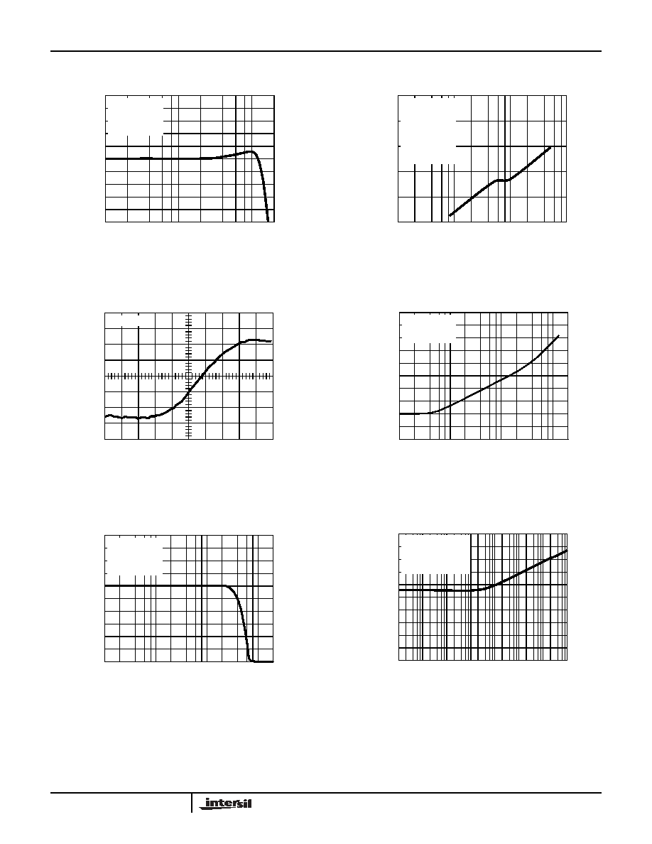
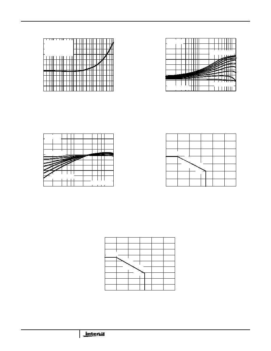
Typical Performance Curves
FIGURE 1. FREQUENCY RESPONSE
FIGURE 2. TOTAL HARMONIC DISTORTION
FIGURE 3. RISE TIME
FIGURE 4. COMMON MODE REJECTION
FIGURE 5. CM AMPLIFIER BANDWIDTH
FIGURE 6. PSRR vs FREQUENCY
5
3
1
-1
-3
-5
1M
10M
100M
FREQUENCY (Hz)
GA
IN (
d
B)
V
GAIN
=0V
V
CTRL
=0V
R
LOAD
=150
X2=OFF
-40
-45
-50
-55
-60
-65
0.1M
1M
10M
100M
FREQUENCY (Hz)
T
HD (dBc)
V
GAIN
=0V
V
CTRL
=0V
V
SS
=+5V
V
EE
=-5V
R
LOAD
=150
X2=OFF
INPUT=0dBm
2ns/DIV
200mV/DIV
V
CTRL
=0V
V
GAIN
=0.35V
X2=ON
100K
1M
10M
100M
FREQUENCY (Hz)
CMRR (dBc)
4
2
0
-2
-4
-6
100K
1M
10M
100M
FREQUENCY (Hz)
GAIN (d
B)
V
GAIN
=0.35V
V
CTRL
=0V
R
LOAD
=150
X2=ON
-20
-40
-60
-80
-100
-120
10
10K
10M 100M
FREQUENCY (Hz)
-PSRR (dB)
100
100K
1K
1M
V
EE
=-5V
V
CTRL
=0V
V
GAIN
=0V
INPUTS ON GND
EL9110
5
FIGURE 7. PSRR vs FREQUENCY
FIGURE 8. GAIN AS THE FUNCTION OF V
CTRL
FIGURE 9. GROUP DELAY AS THE FUNCTION OF THE
FREQUENCY REPONSE CONTROL VOLTAGE
(V
CTRL
)
FIGURE 10. PACKAGE POWER DISSIPATION vs AMBIENT
TEMPERATURE
FIGURE 11. PACKAGE POWER DISSIPATION vs AMBIENT TEMPERATURE
Typical Performance Curves
(Continued)
0
-20
-40
-60
-80
-100
10
10K
10M 100M
FREQUENCY (Hz)
+P
SRR (dB)
100
100K
1K
1M
V
CC
=5V
V
CTRL
=0V
V
GAIN
=0V
INPUTS ON GND
10dB/DIV
1M
FREQUENCY (Hz)
10M
100M
GA
IN (
d
B)
100mV STEP
V
CTRL
=0mV
V
CTRL
=800mV
100mV STEP
V
CTRL
=0mV
V
CTRL
=900mV
1M
100M
FREQUENCY (Hz)
10M
200M
GRO
U
P DE
LA
Y
(ns)
10ns/DIV
791mW
JA
=158
∞C/W
QSO
P16
1.4
1.2
1
0.8
0.6
0.2
0
0
25
50
75
100
150
AMBIENT TEMPERATURE (∞C)
POWER DISS
IP
AT
ION (W)
125
85
JEDEC JESD51-3 LOW EFFECTIVE THERMAL
CONDUCTIVITY TEST BOARD
0.4
1.116W
JA
=112
∞C/W
QSO
P16
1.8
1.6
1
0.8
0.6
0.2
0
0
25
50
75
100
150
AMBIENT TEMPERATURE (∞C)
POWE
R
DI
SSI
PATIO
N
(
W
)
125
85
JEDEC JESD51-7 HIGH EFFECTIVE THERMAL
CONDUCTIVITY TEST BOARD
0.4
1.4
1.2
EL9110