
1
ģ
FN7450.1
EL9111, EL9112
Triple Differential Receiver/Equalizer
The EL9111 and EL9112 are triple channel differential
receivers and equalizers. They contains three high speed
differential receivers with five programmable poles. The
outputs of these pole blocks are then summed into an output
buffer. The equalization length is set with the voltage on a
single pin. The EL9111 and EL9112 also contain a 3-statable
output, enabling multiple devices to be connected in parallel
and used in a multiplexing application.
The gain can be adjusted up or down on each channel by
6dB using its V
GAIN
control signal. In addition, a further 6dB
of gain can be switched in to provide a matched drive into a
cable.
The EL9111 and EL9112 have a bandwidth of 150MHz and
consume just 108mA on Ī5V supply. A single input voltage is
used to set the compensation levels for the required length
of cable.
The EL9111 is a special version of the EL9112 that decodes
syncs encoded onto the common modes of three pairs of
CAT-5 cable by the EL4543. (Refer to the EL4543 datasheet
for details.)
The EL9111 and EL9112 are available in a 28-pin QFN
package and are specified for operation over the full -40įC to
+85įC temperature range.
Features
∑ 150MHz -3dB bandwidth
∑ CAT-5 compensation
- 50MHz @ 1000 ft
- 125MHz @ 500 ft
∑ 108mA supply current
∑ Differential input range 3.2V
∑ Common mode input range -4V to +3.5V
∑ Ī5V supply
∑ Output to within 1.5V of supplies
∑ Available in 28-pin QFN package
∑ Pb-free available (RoHS compliant)
Applications
∑ Twisted-pair receiving/equalizer
∑ KVM (Keyboard/Video/Mouse)
∑ VGA over twisted-pair
∑ Security video
Pinouts
EL9111
(28-PIN QFN)
TOP VIEW
EL9112
(28-PIN QFN)
TOP VIEW
THERMAL
PAD
22
21
20
19
18
17
16
28
27
26
25
24
9
10
11
12
13
1
2
3
4
5
6
7
VSMO_B
VOUT_B
VSPO_B
VSPO_G
VOUT_G
VSMO_G
VSMO_R
VSP
VINM_B
VINP_B
VINM_G
VINP_G
VINM_R
VINP_R
0V
ENABL
E
X2
SYNCREF
VOUT
V
SPO
_R
VCTRL
VR
E
F
V
G
AIN_R
VGAIN_G
8
15
14
23
VSM
V
G
AIN_B
VOUT_R
HO
U
T
THERMAL
PAD
22
21
20
19
18
17
16
28
27
26
25
24
9
10
11
12
13
1
2
3
4
5
6
7
VSMO_B
VOUT_B
VSPO_B
VSPO_G
VOUT_G
VSMO_G
VSMO_R
VSP
VINM_B
VINP_B
VINM_G
VINP_G
VINM_R
VINP_R
0V
ENABL
E
X2
VCM_B
VCM_G
V
SPO
_R
VCTRL
VR
E
F
V
G
AIN_R
VGAIN_G
8
15
14
23
VSM
V
G
AIN_B
VOUT_R
VCM_R
Data Sheet
CAUTION: These devices are sensitive to electrostatic discharge; follow proper IC Handling Procedures.
1-888-INTERSIL or 1-888-352-6832
|
Intersil (and design) is a registered trademark of Intersil Americas Inc.
Copyright Intersil Americas Inc. 2005. All Rights Reserved
All other trademarks mentioned are the property of their respective owners.
May 17, 2005
2
FN7450.1
May 17, 2005
Ordering Information
PART
NUMBER
PACKAGE
TAPE &
REEL
PKG. DWG. #
PART
NUMBER
PACKAGE
TAPE &
REEL
PKG. DWG. #
EL9111IL
28-Pin QFN
-
MDP0046
EL9112IL
28-Pin QFN
-
MDP0046
EL9111IL-T7
28-Pin QFN
7"
MDP0046
EL9112IL-T7
28-Pin QFN
7"
MDP0046
EL9111IL-T13
28-Pin QFN
13"
MDP0046
EL9112IL-T13
28-Pin QFN
13"
MDP0046
EL9111ILZ
(Note)
28-Pin QFN
(Pb-Free)
-
MDP0046
EL9112ILZ
(Note)
28-Pin QFN
(Pb-Free)
-
MDP0046
EL9111ILZ-T7
(Note)
28-Pin QFN
(Pb-Free)
7"
MDP0046
EL9112ILZ-T7
(Note)
28-Pin QFN
(Pb-Free)
7"
MDP0046
EL9111ILZ-T13
(Note)
28-Pin QFN
(Pb-Free)
13"
MDP0046
EL9112ILZ-T13
(Note)
28-Pin QFN
(Pb-Free)
13"
MDP0046
NOTE: Intersil Pb-free products employ special Pb-free material sets; molding compounds/die attach materials and 100% matte tin plate termination
finish, which are RoHS compliant and compatible with both SnPb and Pb-free soldering operations. Intersil Pb-free products are MSL classified at Pb-
free peak reflow temperatures that meet or exceed the Pb-free requirements of IPC/JEDEC J STD-020.
EL9111, EL9112
3
FN7450.1
May 17, 2005
IMPORTANT NOTE: All parameters having Min/Max specifications are guaranteed. Typ values are for information purposes only. Unless otherwise noted, all tests are
at the specified temperature and are pulsed tests, therefore: T
J
= T
C
= T
A
Absolute Maximum Ratings
(T
A
= 25įC)
Supply Voltage between V
S
+ and V
S
- . . . . . . . . . . . . . . . . . . . . .12V
Maximum Continuous Output Current per Channel. . . . . . . . . 30mA
Power Dissipation . . . . . . . . . . . . . . . . . . . . . . . . . . . . . See Curves
Pin Voltages . . . . . . . . . . . . . . . . . . . . . . . . . V
S
- -0.5V to V
S
+ +0.5V
Storage Temperature . . . . . . . . . . . . . . . . . . . . . . . .-65įC to +150įC
Ambient Operating Temperature . . . . . . . . . . . . . . . .-40įC to +85įC
Die Junction Temperature . . . . . . . . . . . . . . . . . . . . . . . . . . . . 150įC
CAUTION: Stresses above those listed in "Absolute Maximum Ratings" may cause permanent damage to the device. This is a stress only rating and operation of the
device at these or any other conditions above those indicated in the operational sections of this specification is not implied.
Electrical Specifications
V
SA
+
= V
A
+
= +5V, V
SA
-
= V
A
-
= -5V, T
A
= 25įC, unless otherwise specified.
PARAMETER
DESCRIPTION
CONDITIONS
MIN
TYP
MAX
UNIT
AC PERFORMANCE
BW
Bandwidth
(See Figure 1)
150
MHz
SR
Slew Rate
V
IN
= -1V to +1V, V
G
= 0.39, V
C
= 0,
R
L
= 75 + 75
1.5
kV/Ķs
THD
Total Harmonic Distortion
10MHz 2V
P-P
out, V
G
= 1V, X2 gain, V
C
= 0
-50
dBc
DC PERFORMANCE
V(V
OUT
)
OS
Offset Voltage
X2 = high, no equalization
-110
-10
+78
mV
V
OS
Channel-to-Channel Offset Matching X2 = high, no equalization
-100
0
+100
mV
INPUT CHARACTERISTICS
CMIR
Common-mode Input Range
-4/+3.5
V
O
NOISE
Output Noise
V
G
= 0V, V
C
= 0V, X2 = HIGH, R
LOAD
= 150
,
Input 50
to GND, 10MHz
-110
dBm
CMRR
Common-mode Rejection Ratio
Measured at 10kHz
-80
dB
CMRR
Common-mode Rejection Ratio
Measured at 10MHz
-55
dB
CMBW
CM Amplifier Bandwidth
10K || 10pF load
50
MHz
CM
SLEW
CM Slew Rate
Measured @ +1V to -1V
100
V/Ķs
C
INDIFF
Differential Input Capacitance
Capacitance V
INP
to V
INM
600
fF
R
INDIFF
Differential Input Resistance
Resistance V
INP
to V
INM
1
2.4
M
C
INCM
CM Input Capacitance
Capacitance V
INP
= V
INM
to GND
1.2
pF
R
INCM
CM Input Resistance
Resistance V
INP
= V
INM
to GND
1
2.8
M
+I
IN
Positive Input Current
DC bias @ V
INP
= V
INM
= 0V
1
ĶA
-I
IN
Negative Input Current
DC bias @ V
INP
= V
INM
= 0V
1
ĶA
V
INDIFF
Differential Input Range
V
INP
- V
INM
when slope gain falls to 0.9
2.5
3.2
V
OUTPUT CHARACTERISTICS
V(V
OUT
)
Output Voltage Swing
R
L
= 150
Ī3.5
V
I(V
OUT
)
Output Drive Current
R
L
= 10
, V
INP
= 1V, V
INM
= 0V, X2 = high,
V
G
= 0.39
50
60
mA
R(V
CM
)
CM Output Resistance of
VCM_R/G/B (EL9112 only)
at 100kHz
30
Gain
Gain
V
C
= 0, V
G
= 0.39, X2 = 5, R
L
= 150
0.85
1.0
1.1
Gain
Channel-to-Channel Gain Matching
V
C
= 0, V
G
= 0.39, X2 = 5, R
L
= 150
3
6
%
V(SYNC)
HI
High Level output on V/H
OUT
(EL9111 only)
V(V
SP
)
- 0.1V
V(V
SP
)
EL9111, EL9112
4
FN7450.1
May 17, 2005
V(SYNC)
LO
Low Level output on V/H
OUT
(EL9111 only)
0
V(SYNC
REF)
+ 0.1V
SUPPLY
I
SON
Supply Current per Channel
V
ENBL
= 5, V
INM
= 0
32
36
39
mA
I
SOFF
Supply Current per Channel
V
ENBL
= 0, V
INM
= 0
0.2
0.4
mA
PSRR
Power Supply Rejection Ratio
DC to 100kHz, Ī5V supply
65
dB
LOGIC CONTROL PINS (ENABLE, X2)
V
HI
Logic High Level
V
IN
- V
LOGIC
ref for guaranteed high level
1.35
V
V
LOW
Logic Low Level
V
IN
- V
LOGIC
ref for guaranteed low level
0.8
V
I
LOGICH
Logic High Input Current
V
IN
= 5V, V
LOGIC
= 0V
50
ĶA
I
LOGICL
Logic Low Input Current
V
IN
= 0V, V
LOGIC
= 0V
15
ĶA
Electrical Specifications
V
SA
+
= V
A
+
= +5V, V
SA
-
= V
A
-
= -5V, T
A
= 25įC, unless otherwise specified. (Continued)
PARAMETER
DESCRIPTION
CONDITIONS
MIN
TYP
MAX
UNIT
Pin Descriptions
PIN
NUMBER
EL9111IL
PIN NAME
EL9111IL
PIN FUNCTION
EL9112IL
PIN NAME
EL9112IL
PIN FUNCTION
1
VSMO_B
-5V to blue output buffer
VSMO_B
-5V to blue output buffer
2
VOUT_B
Blue output voltage referenced to 0V pin
VOUT_B
Blue output voltage referenced to 0V pin
3
VSPO_B
+5V to blue output buffer
VSPO_B
+5V to blue output buffer
4
VSPO_G
+5V to green output buffer
VSPO_G
+5V to green output buffer
5
VOUT_G
Green output voltage referenced to 0V pin
VOUT_G
Green output voltage referenced to 0V pin
6
VSMO_G
-5V to green output buffer
VSMO_G
-5V to green output buffer
7
VSMO_R
-5V to red output buffer
VSMO_R
-5V to red output buffer
8
VOUT_R
Red output voltage referenced to 0V pin
VOUT_R
Red output voltage referenced to 0V pin
9
VSPO_R
+5V to red output buffer
VSPO_R
+5V to red output buffer
10
VCTRL
Equalization control voltage (0V to 1V)
VCTRL
Equalization control voltage (0V to 1V)
11
VREF
Reference voltage for logic signals, V
CTRL
and
V
GAIN
pins
VREF
Reference voltage for logic signals, V
CTRL
and
V
GAIN
pins
12
VGAIN_R
Red channel gain voltage (0V to 1V)
VGAIN_R
Red channel gain voltage (0V to 1V)
13
VGAIN_G
Green channel gain voltage (0V to 1V)
VGAIN_G
Green channel gain voltage (0V to 1V)
14
VGAIN_B
Blue channel gain voltage (0V to 1V)
VGAIN_B
Blue channel gain voltage (0V to 1V)
15
VSM
-5V to core of chip
VSM
-5V to core of chip
16
VINP_R
Red positive differential input
VINP_R
Red positive differential input
17
VINM_R
Red negative differential input
VINM_R
Red negative differential input
18
VINP_G
Green positive differential input
VINP_G
Green positive differential input
19
VINM_G
Green negative differential input
VINM_G
Green negative differential input
20
VINP_B
Blue positive differential input
VINP_B
Blue positive differential input
21
VINM_B
Blue negative differential input
VINM_B
Blue negative differential input
22
VSP
+5V to core of chip
VSP
+5V to core of chip
23
HOUT
Decoded Horizontal sync referenced to
SYNCREF
VCM_R
Red common-mode voltage at inputs
24
VOUT
Decoded Vertical sync referenced to SYNCREF
VCM_G
Green common-mode voltage at inputs
25
SYNCREF
Reference level for H
OUT
and V
OUT
logic outputs
VCM_B
Blue common-mode voltage at inputs
EL9111, EL9112

5
FN7450.1
May 17, 2005
26
X2
Logic signal for x1/x2 output gain setting
X2
Logic signal for x1/x2 output gain setting
27
ENABLE
Chip enable logic signal
ENABLE
Chip enable logic signal
28
0V
0V reference for output voltage
0V
0V reference for output voltage
Pin Descriptions
(Continued)
PIN
NUMBER
EL9111IL
PIN NAME
EL9111IL
PIN FUNCTION
EL9112IL
PIN NAME
EL9112IL
PIN FUNCTION
Typical Performance Curves
FIGURE 1. FREQUENCY RESPONSE OF ALL CHANNELS
FIGURE 2. GAIN vs FREQUENCY ALL CHANNELS
FIGURE 3. GAIN vs FREQUENCY FOR VARIOUS V
CTRL
FIGURE 4. GAIN vs FREQUENCY FOR VARIOUS V
CTRL
&
V
GAIN
1M
10M
100M 200M
5
3
1
-1
-3
-5
X
2
=LOW
V
GAIN
=0V
V
CTRL
=0V
R
LOAD
=150
FREQUENCY (Hz)
G
A
IN
(
d
B)
EL9111, EL9112

6
FN7450.1
May 17, 2005
FIGURE 5. GAIN vs FREQUENCY FOR VARIOUS V
CTRL
&
CABLE LENGTHS
FIGURE 6. CHANNEL MISMATCH
FIGURE 7. GROUP DELAY vs FREQUENCY FOR VARIOUS
V
CTRL
FIGURE 8. OUTPUT NOISE
FIGURE 9. OFFSET vs V
CTRL
FIGURE 10. DC GAIN vs V
GAIN
Typical Performance Curves
(Continued)
EL9111, EL9112

7
FN7450.1
May 17, 2005
FIGURE 11. COMMON-MODE REJECTION
FIGURE 12. CM AMPLIFIER BANDWIDTH
FIGURE 13. (+)PSRR vs FREQUENCY
FIGURE 14. (-)PSRR vs FREQUENCY
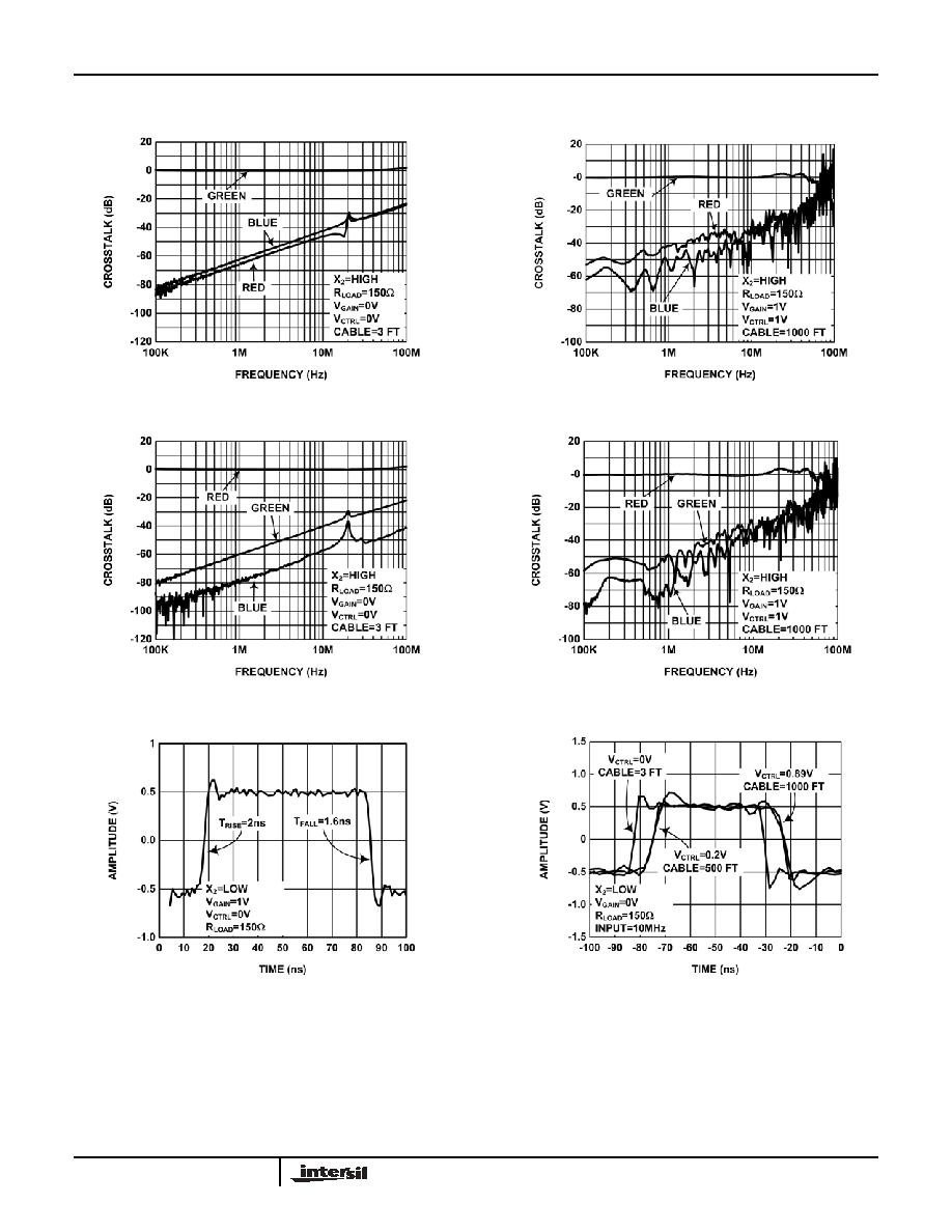
FIGURE 15. BLUE CROSSTALK
FIGURE 16. BLUE CROSSTALK
Typical Performance Curves
(Continued)
100K
1M
10M
100M
-10
-20
-40
-60
-80
-100
V
GAIN
=0.35V
(ALL CHANNELS)
V
CTRL
=0V
X
2
=HIGH
FREQUENCY (Hz)
CMRR (dB)
100K
1M
10M
100M
4
2
0
-2
-4
-6
V
GAIN
=0.35V
(ALL CHANNELS)
V
CTRL
=0V
R
LOAD
=150
X
2
=HIGH
FREQUENCY (Hz)
GA
IN (
d
B)
10
1K
100K
100M
0
-20
-40
-60
-80
-100
V
CC
=5V
V
CTRL
=0V
V
GAIN
=0V
(ALL CHANNELS)
INPUTS ON GND
FREQUENCY (Hz)
+PSRR (dB)
100
10K
1M
10M
10
1K
100K
100M
-20
-40
-60
-80
-100
-120
V
EE
=-5V
V
CTRL
=0V
V
GAIN
=0V
(ALL CHANNELS)
INPUTS ON GND
FREQUENCY (Hz)
-P
SRR (dB
)
100
10K
1M
10M
EL9111, EL9112
8
FN7450.1
May 17, 2005
FIGURE 17. GREEN CROSSTALK
FIGURE 18. GREEN CROSSTALK
FIGURE 19. RED CROSSTALK
FIGURE 20. RED CROSSTALK
FIGURE 21. RISE TIME AND FALL TIME
FIGURE 22. PULSE RESPONSE FOR VARIOUS CABLE
LENGTHS
Typical Performance Curves
(Continued)
EL9111, EL9112

9
FN7450.1
May 17, 2005
FIGURE 23. TOTAL HARMONIC DISTORTION
FIGURE 24. PACKAGE POWER DISSIPATION vs AMBIENT
TEMPERATURE
FIGURE 25. PACKAGE POWER DISSIPATION vs AMBIENT
TEMPERATURE
Typical Performance Curves
(Continued)
JEDEC JESD51-3 LOW EFFECTIVE THERMAL
CONDUCTIVITY TEST BOARD
893mW
JA
=14
0įC
/W
QF
N28
0
50
85
150
1.2
0.8
0.6
0.4
0.2
0
AMBIENT TEMPERATURE (įC)
P
O
WER DIS
S
IP
A
T
ION
(
W
)
25
75
100
125
1
JEDEC JESD51-7 HIGH EFFECTIVE THERMAL
CONDUCTIVITY TEST BOARD - QFN EXPOSED
DIEPAD SOLDERED TO PCB PER JESD51-5
JA
=37
įC/W
QF
N28
3.378W
0
50
85
150
4.5
3.5
2.5
1.5
0.5
0
AMBIENT TEMPERATURE (įC)
PO
WER D
I
SS
IP
A
T
IO
N
(W)
25
75
100
125
4
2
1
3
EL9111, EL9112
10
FN7450.1
May 17, 2005
Applications Information
Logic Control
The EL9112 has two logical input pins, Chip Enable
(ENABLE) and Switch Gain (X2). The logic circuits all have a
nominal threshold of 1.1V above the potential of the logic
reference pin (VREF). In most applications it is expected that
this chip will run from a +5V, 0V, -5V supply system with logic
being run between 0V and +5V. In this case the logic
reference voltage should be tied to the 0V supply. If the logic
is referenced to the -5V rail, then the logic reference should
be connected to -5V. The logic reference pin sources about
60ĶA and this will rise to about 200ĶA if all inputs are true
(positive).
The logic inputs all source up to 10ĶA when they are held at
the logic reference level. When taken positive, the inputs
sink a current dependent on the high level, up to 50ĶA for a
high level 5V above the reference level.
The logic inputs, if not used, should be tied to the
appropriate voltage in order to define their state.
Control Reference and Signal Reference
Analog control voltages are required to set the equalizer and
contrast levels. These signals are voltages in the range 0V -
1V, which are referenced to the control reference pin. It is
expected that the control reference pin will be tied to 0V and
the control voltage will vary from 0V to 1V. It is; however,
acceptable to connect the control reference to any potential
between -5V and 0V to which the control voltages are
referenced.
The control voltage pins themselves are high impedance.
The control reference pin will source between 0ĶA and
200ĶA depending on the control voltages being applied.
The control reference and logic reference effectively remove
the necessity for the 0V rail and operation from Ī5V (or 0V
and 10V) only is possible. However we still need a further
reference to define the 0V level of the single ended output
signal. The reference for the output signal is provided by the
0V pin. The output stage cannot pull fully up or down to
either supply so it is important that the reference is
positioned to allow full output swing. The 0V reference
should be tied to a 'quiet ground' as any noise on this pin is
transferred directly to the output. The 0V pin is a high
impedance pin and draws dc bias currents of a few ĶA and
similar levels of AC current.
Equalizing
When transmitting a signal across a twisted pair cable, it is
found that the high frequency (above 1MHz) information is
attenuated more significantly than the information at low
frequencies. The attenuation is predominantly due to
resistive skin effect losses and has a loss curve which
depends on the resistivity of the conductor, surface condition
of the wire and the wire diameter. For the range of high
performance twisted pair cables based on 24awg copper
wire (CAT-5 etc.) these parameters vary only a little between
cable types, and in general cables exhibit the same
frequency dependence of loss. (The lower loss cables can
be compared with somewhat longer lengths of their more
lossy brothers.) This enables a single equalizing law
equation to be built into the EL9112.
With a control voltage applied between pins V
CTRL
and
V
REF
, the frequency dependence of the equalization is
shown in Figure 8. The equalization matches the cable loss
up to about 100MHz. Above this, system gain is rolled off
rapidly to reduce noise bandwidth. The roll-off occurs more
rapidly for higher control voltages, thus the system (cable +
equalizer) bandwidth reduces as the cable length increases.
This is desirable, as noise becomes an increasing issue as
the equalization increases.
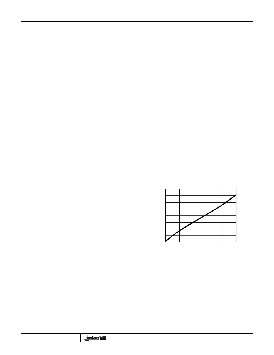
Contrast
By varying the voltage between pins V
GAIN
and V
REF
, the
gain of the signal path can be changed in the ratio 4:1. The
gain change varies almost linearly with control voltage. For
normal operation it is anticipated the X2 mode will be
selected and the output load will be back matched. A unity
gain to the output load will then be achieved with a gain
control voltage of about 0.35V. This allows the gain to be
trimmed up or down by 6dB to compensate for any gain/loss
errors that affect the contrast of the video signal. Figure 26
shows an example plot of the gain to the load with gain
control voltage.
FIGURE 26. VARIATION OF GAIN WITH GAIN CONTROL
VOLTAGE
C
ommon Mode Sync Decoding
The EL9111 features common mode decoding to allow
horizontal and vertical synchronization information, which
has been encoded on the three differential inputs by the
EL4543, to be decoded. The entire RGB video signal can
therefore be transmitted, along with the associated
synchronization information, by using just three twisted
pairs.
0
0.8
V
GAIN
0.4
1
2
1.8
1.4
1
0.6
0.4
GAI
N
(
V
)
0.6
0.2
1.6
1.2
0.8
EL9111, EL9112

11
FN7450.1
May 17, 2005
Decoding is based on the EL4543 encoding scheme, as
described in Figure 27 and Table 1. The scheme is a three-
level system, which has been designed such that the sum of
the common mode voltages results in a fixed average DC
level with no AC content. This eliminates the effect of EMI
radiation into the common mode signals along the twisted
pairs of the cable
The common mode voltages are initially extracted by the
EL9111 from the three input pairs. These are then passed to
an internal logic decoding block to provide Horizontal and
Vertical sync output signals (H
OUT
and V
OUT
).
FIGURE 27. H & V SYNCS ENCODED
TABLE 1. H AND V SYNC DECODING
RED CM
GREEN CM
BLUE CM
H
SYNC
V
SYNC
Mid
High
Low
Low
Low
High
Low
Mid
Low
High
Low
High
Mid
High
Low
Mid
Low
High
High High
NOTE: Level `Mid' is halfway between `High' and `Low'
TIME (0.5ms/DIV)
VOLTA
GE
(0.
5
V/
DIV
)
BLUE CM
OUT (CH A)
GREEN CM
OUT (CH B)
RED CM
OUT (CH C)
V
SYNC
H
SYNC
VO
LTA
GE
(2.
5
V/
DIV
)
EL9111, EL9112

12
All Intersil U.S. products are manufactured, assembled and tested utilizing ISO9000 quality systems.
Intersil Corporation's quality certifications can be viewed at www.intersil.com/design/quality
Intersil products are sold by description only. Intersil Corporation reserves the right to make changes in circuit design, software and/or specifications at any time without
notice. Accordingly, the reader is cautioned to verify that data sheets are current before placing orders. Information furnished by Intersil is believed to be accurate and
reliable. However, no responsibility is assumed by Intersil or its subsidiaries for its use; nor for any infringements of patents or other rights of third parties which may result
from its use. No license is granted by implication or otherwise under any patent or patent rights of Intersil or its subsidiaries.
For information regarding Intersil Corporation and its products, see www.intersil.com
FN7450.1
May 17, 2005
Package Outline Drawing
NOTE: The package drawing shown here may not be the latest version. To check the latest revision, please refer to the Intersil website at
http://www.intersil.com/design/packages/index.asp
EL9111, EL9112