1
Æ
FN7438.0
CAUTION: These devices are sensitive to electrostatic discharge; follow proper IC Handling Procedures.
1-888-INTERSIL or 321-724-7143
|
Intersil (and design) is a registered trademark of Intersil Americas Inc.
Copyright © Intersil Americas Inc. 2005. All Rights Reserved.
All other trademarks mentioned are the property of their respective owners.
EL9200, EL9201, EL9202
Programmable V
COM
The EL9200, EL9201, and EL9202 represent programmable
V
COM
amplifiers for use in TFT-LCD displays. Featuring 1,
2, and 4 channels of V
COM
amplification, respectively, each
device features just a single programmable current source
for adding offset to one V
COM
output. This current source is
programmable using a single wire interface to one of 128
levels. The value is stored on an internal EEPROM memory.
The EL9200 is available in the 12-pin DFN package and the
EL9201 and EL9202 are available in 24-pin QFN packages.
All are specified for operation over the -40∞C to +85∞C
temperature range.
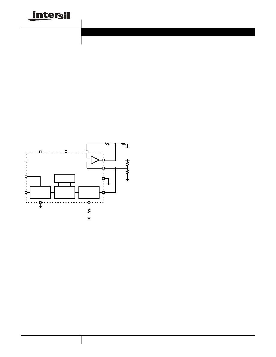
Typical Block Diagram
Features
∑ 128 step adjustable sink current
∑ EEPROM memory
∑ 2-pin adjustment and disable
∑ Single, dual or quad amplifiers
- 44MHz bandwidth
- 80V/µs slew rate
- 60mA continuous output
- 180mA peak output
∑ Up to 18V operation
∑ 2.6V to 3.6V logic control
∑ Pb-free available (RoHS compliant)
Applications
∑ TFT-LCD V
COM
supplies for
- LCD-TVs
- LCD monitors
-
+
EEPROM
CONTROL
UP/DOWN
COUNTER
ANALOG
POT
CTL
CE
V
SD
A
VDD
GND
SET
R
SET
I
OUT
INP
V
OUT
INN
R
F
R
G
R
1
R
2
A
VDD
V
S
+
GND
Data Sheet
April 7, 2005
2
FN7438.0
April 7, 2005
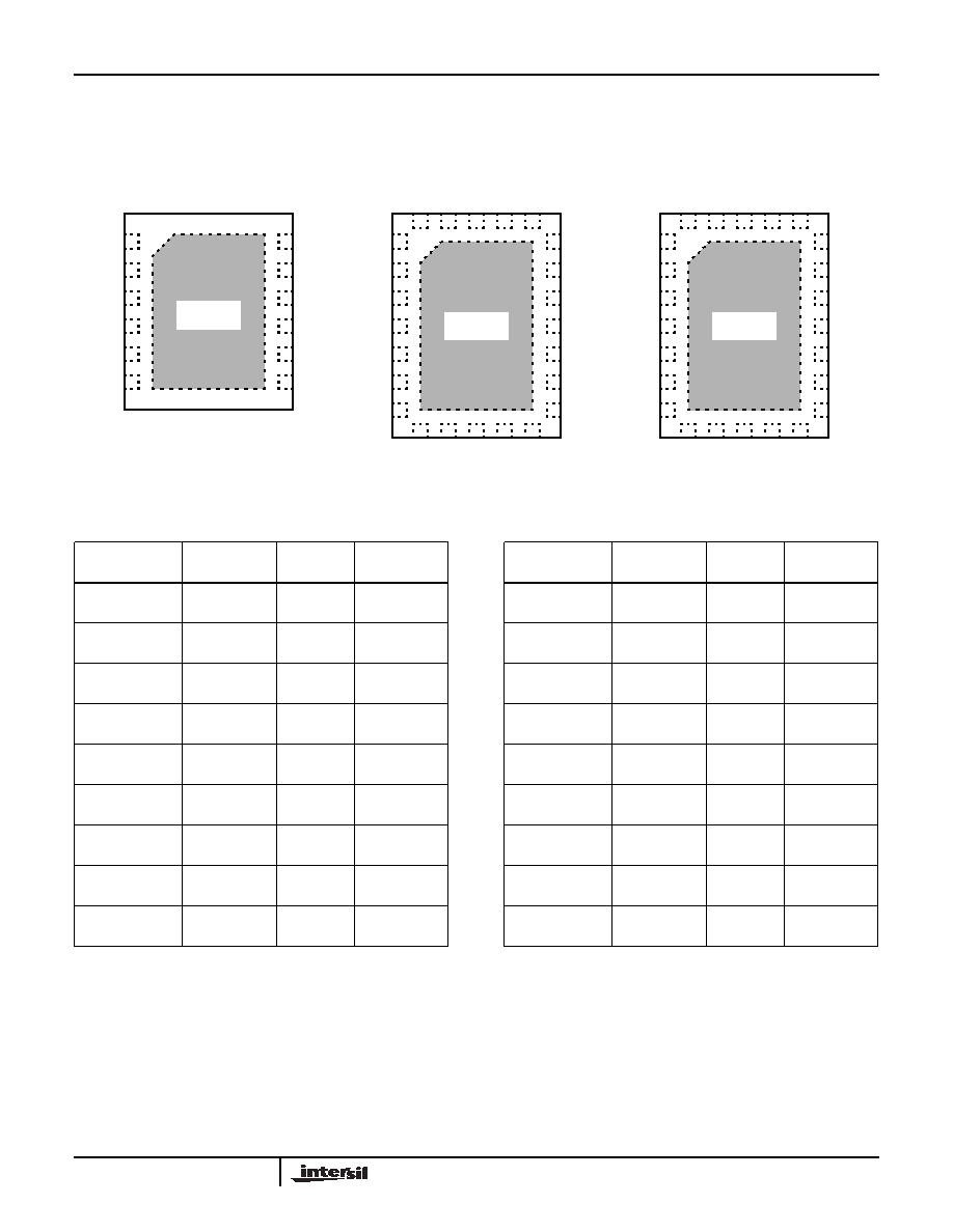
Pinouts
EL9200
(12-PIN DFN)
TOP VIEW
EL9201
(24-PIN QFN)
TOP VIEW
EL9202
(24-PIN QFN)
TOP VIEW
12
11
10
9
8
7
1
2
3
4
5
6
THERMAL
PAD
VINA-
GND
VINA+
IOUT
AVDD
GND
VS+
VOUTA
SET
CE
CTL
VSD
19
18
17
16
15
14
13
24
23
22
21
20
8
9
10
11
12
1
2
3
4
5
6
7
NC
NC
VINB+
IOUT
NC
AVDD
GND
NC
VOUTA
VS+
VOUTB
VINB-
SET
CE
NC
GND
NC
VINA+
VINA-
NC
NC
NC
VSD
CT
L
THERMAL
PAD
19
18
17
16
15
14
13
24
23
22
21
20
8
9
10
11
12
1
2
3
4
5
6
7
VOUTA
VOUTD
VIND-
NC
VIND+
AVDD
CTL
VOUTB
VOUTC
VINC-
NC
VINC+
GND
AVDD
VINA-
VINA+
VS
+
VINB+
VINB-
CE
NC
SET
IO
UT
NC
THERMAL
PAD
Ordering Information
PART NUMBER
PACKAGE
TAPE &
REEL
PKG. DWG. #
PART NUMBER
PACKAGE
TAPE &
REEL
PKG. DWG. #
EL9200IL
12-Pin DFN
-
MDP0047
EL9201ILZ
(See Note)
24-Pin QFN
(Pb-Free)
-
MDP0046
EL9200IL-T7
12-Pin DFN
7"
MDP0047
EL9201ILZ-T7
(See Note)
24-Pin QFN
(Pb-Free)
7"
MDP0046
EL9200IL-T13
12-Pin DFN
13"
MDP0047
EL9201ILZ-T13
(See Note)
24-Pin QFN
(Pb-Free)
13"
MDP0046
EL9200ILZ
(See Note)
12-Pin DFN
(Pb-Free)
-
MDP0047
EL9202IL
24-Pin QFN
-
MDP0046
EL9200ILZ-T7
(See Note)
12-Pin DFN
(Pb-Free)
7"
MDP0047
EL9202IL-T7
24-Pin QFN
7"
MDP0046
EL9200ILZ-T13
(See Note)
12-Pin DFN
(Pb-Free)
13"
MDP0047
EL9202IL-T13
24-Pin QFN
13"
MDP0046
EL9201IL
24-Pin QFN
-
MDP0046
EL9202ILZ
(See Note)
24-Pin QFN
(Pb-Free)
-
MDP0046
EL9201IL-T7
24-Pin QFN
7"
MDP0046
EL9202ILZ-T7
(See Note)
24-Pin QFN
(Pb-Free)
7"
MDP0046
EL9201IL-T13
24-Pin QFN
13"
MDP0046
EL9202ILZ-T13
(See Note)
24-Pin QFN
(Pb-Free)
13"
MDP0046
NOTE: Intersil Pb-free products employ special Pb-free material sets; molding compounds/die attach materials and 100% matte tin plate termination
finish, which are RoHS compliant and compatible with both SnPb and Pb-free soldering operations. Intersil Pb-free products are MSL classified at
Pb-free peak reflow temperatures that meet or exceed the Pb-free requirements of IPC/JEDEC J STD-020.
EL9200, EL9201, EL9202
3
FN7438.0
April 7, 2005
Absolute Maximum Ratings
(T
A
= 25∞C)
V
S
+
Supply Voltage between V
S
+ and GND . . . . . . . . . . . . . .18V
Supply Voltage between V
SD
and GND . . . . . . . . . . . . . . . . . . . .4V
Maximum Continuous Output Current . . . . . . . . . . . . . . . . . . . 65mA
Input Voltages to GND
SET, CE . . . . . . . . . . . . . . . . . . . . . . . . . . . . . . . . . . . -0.3V to +4V
CTL. . . . . . . . . . . . . . . . . . . . . . . . . . . . . . . . . . . . . . -0.3V to +16V
Output Voltages to GND
OUT . . . . . . . . . . . . . . . . . . . . . . . . . . . . . . . . . . . . . -0.3V to +20V
A
VDD
. . . . . . . . . . . . . . . . . . . . . . . . . . . . . . . . . . . . . . -0.3V to +20V
ESD Rating - HBM for Device . . . . . . . . . . . . . . . . . . . . . . . . . . . 2kV
Ambient Operating Temperature . . . . . . . . . . . . . . . .-40∞C to +85∞C
Maximum Die Temperature . . . . . . . . . . . . . . . . . . . . . . . . . . +150∞C
Storage Temperature . . . . . . . . . . . . . . . . . . . . . . . .-65∞C to +150∞C
Maximum Lead Temperature (Soldering 10s) . . . . . . . . . . . . +300∞C
CAUTION: Stresses above those listed in "Absolute Maximum Ratings" may cause permanent damage to the device. This is a stress only rating and operation of the
device at these or any other conditions above those indicated in the operational sections of this specification is not implied.
IMPORTANT NOTE: All parameters having Min/Max specifications are guaranteed. Typical values are for information purposes only. Unless otherwise noted, all tests
are at the specified temperature and are pulsed tests, therefore: T
J
= T
C
= T
A
Electrical Specifications
V
SD
= 3V, V
S
+
= 15V, A
VDD
= 15V, R
SET
= 24.9k
, and T
A
= 25∞C unless otherwise specified
PARAMETER
DESCRIPTION
CONDITION
MIN
TYP
MAX
UNIT
V
S+
Supply Voltage
4.5
16.5
V
I
S+
Quiescent Current
EL9200
3.8
4.8
mA
EL9201
7.6
9.6
mA
EL9202
10.5
16
mA
V
SD
Logic Supply Voltage
For programming
3
3.6
V
For operation
2.6
3.6
V
I
SD
Quiescent Logic Current
CE = 3.6V
50
µA
CE = GND
25
µA
Program (charge pump current) (Note 1)
23
mA
Read (Note 1)
3
mA
I
ADD
Supply Current
Note 2
25
µA
CTL
IH
CTL High Voltage
2.6V < V
SD
< 3.6V
0.7*V
SD
0.8*V
SD
V
CTL
IL
CTL Low Voltage
2.6V < V
SD
< 3.6V
0.2*V
SD
0.3*V
SD
V
CTL
IHRPW
CTL High Rejected Pulse Width
20
µs
CTL
ILRPW
CTL Low Rejected Pulse Width
20
µs
CTL
IHMPW
CTL High Minimum Pulse Width
200
µs
CTL
ILMPW
CTL Low Minimum Pulse Width
200
µs
CTL
MTC
CTL Minimum Time Between Counts
10
µs
ICTL
CTL Input Current
CTL = GND
10
µA
CTL = V
SD
10
µA
CTL
CAP
CTL Input Capacitance
10
pF
CE
IL
CE Input Low Voltage
2.6V < V
SD
< 3.6V
0.4
V
CE
IH
CE Input High Voltage
2.6V < V
SD
< 3.6V
1.6
V
CE
ST
CE Minimum Start Up Time
(Note 1)
1
m
s
CTL
PROM
CTL EEPROM Program Voltage
2.6V < V
SD
< 3.6V (Note 2)
4.9
15.75
V
CTL
PT
CTL EEPROM Programming Signal
Time
> 4.9V
200
µs
P
T
Programming Time
100
ms
EE
WC
EE Write Cycles
Guaranteed by design
1000
cycles
SET
DN
SET Differential Nonlinearity
Monotonic over-temperature
±1
LSB
EL9200, EL9201, EL9202
4
FN7438.0
April 7, 2005
SET
ZSE
SET Zero-Scale Error
Note 3
±2
LSB
SET
FSE
SET Full-Scale Error
Note 3
±8
LSB
I
SET
SET Current
Through R
SET
(Note 1)
120
µA
SET
ER
SET External Resistance
To GND, A
VDD
= 20V (Note 1)
10
200
k
To GND, A
VDD
= 4.5V (Note 1)
2.25
45
k
A
VDD
to SET
A
VDD
to SET Voltage Attenuation
1:20
V/V
OUT
ST
OUT Settling Time
To
±0.5 LSB error band (Note 1)
20
µs
V
OUT
OUT Voltage Range
(Note 1)
V
SET
+
0.5V
13
V
OUT
VD
OUT Voltage Drift
(Note 1)
10
mV
AMPLIFIER CHARACTERISTICS
INPUT CHARACTERISTICS
V
OS
Input Offset Voltage
V
CM
= 0V
3
15
mV
TCV
OS
Average Offset Voltage Drift (Note 1)
7
µV/∞C
I
B
Input Bias Current
V
CM
= 0V
2
60
nA
R
IN
Input Impedance
1
G
C
IN
Input Capacitance
2
pF
CMRR
Common-Mode Rejection Ratio
For V
IN
from -5.5V to +5.5V
50
70
dB
A
VOL
Open-Loop Gain
-4.5V
V
OUT
+4.5V
60
70
dB
OUTPUT CHARACTERISTICS
V
OL
Output Swing Low
R
L
= 1.5k
to 0
0.09
0.15
V
V
OH
Output Swing High
14.85
14.9
V
I
SC
Short-Circuit Current
±150
±180
mA
I
OUT
Output Current
±65
mA
POWER SUPPLY PERFORMANCE
PSRR
Power Supply Rejection Ratio
V
S+
is moved from 4.5V to 15.5V
55
80
dB
DYNAMIC PERFORMANCE
SR
Slew Rate (Note 4)
-4.0V
V
OUT
4.0V, 20% to 80%
60
80
V/µs
t
S
Settling to +0.1% (A
V
= +1)
(A
V
= +1), V
OUT
= 2V step
80
ns
BW
-3dB Bandwidth
44
MHz
GBWP
Gain-Bandwidth Product
32
MHz
PM
Phase Margin
50
∞
CS
Channel Separation
f = 5MHz (EL9201 & EL9202 only)
110
dB
d
G
Differential Gain (Note 5)
R
F
= R
G
= 1k
and V
OUT
= 1.4V
0.17
%
d
P
Differential Phase (Note 5)
R
F
= R
G
= 1k
and V
OUT
= 1.4V
0.24
∞
NOTES:
1. Simulated and determined via design and not directly tested
2. Tested at A
VDD
= 20V
3. Wafer sort only
4. NTSC signal generator used
Electrical Specifications
V
SD
= 3V, V
S
+
= 15V, A
VDD
= 15V, R
SET
= 24.9k
, and T
A
= 25∞C unless otherwise specified
PARAMETER
DESCRIPTION
CONDITION
MIN
TYP
MAX
UNIT
EL9200, EL9201, EL9202
5
FN7438.0
April 7, 2005
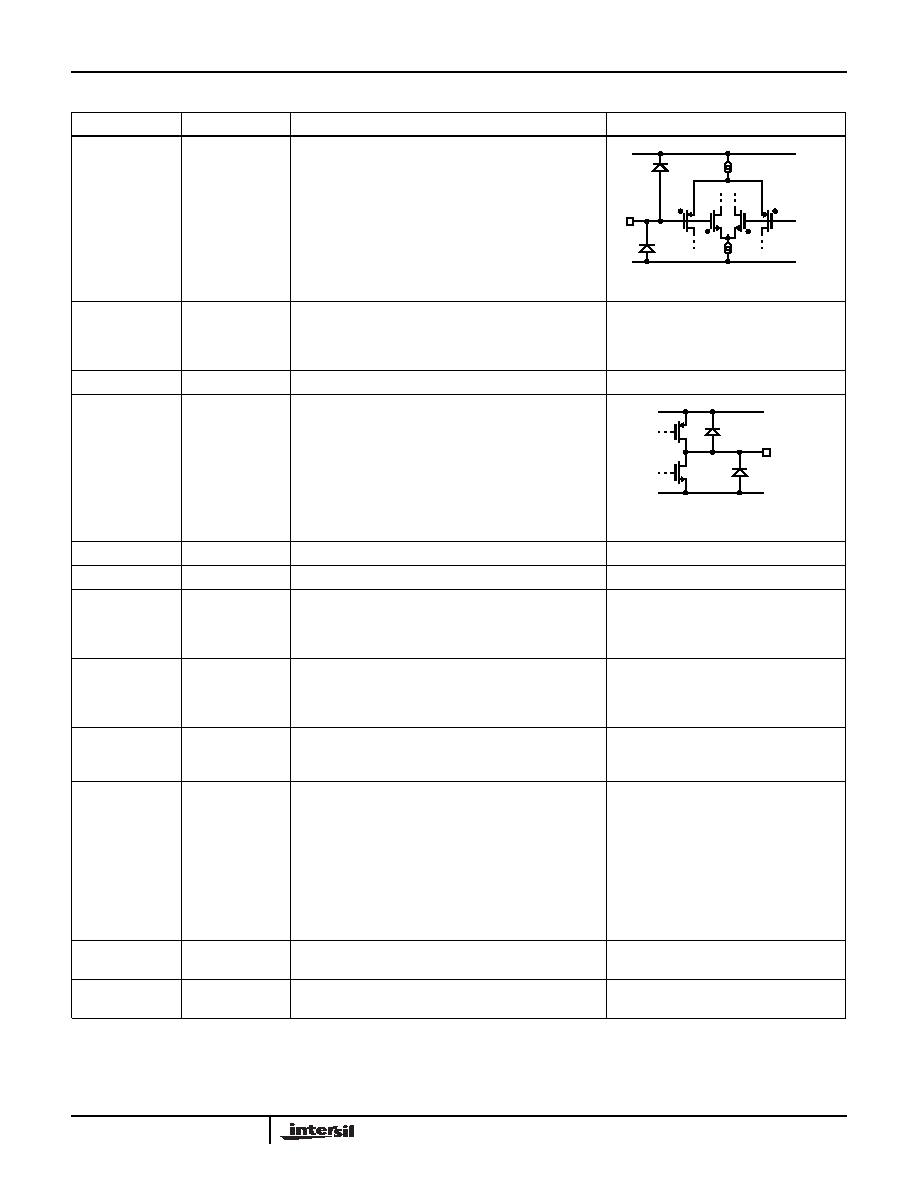
Pin Descriptions
PIN
IN/OUT
DESCRIPTION
EQUIVALENT CIRCUIT
VINX-
Input
Amplifier X inverting input, where:
X = A for EL9200
X = A, B for EL9201
X = A, B, C, D for EL9202
VINX+
Input
Amplifier X non-inverting input, where:
X = A for EL9200
X = A, B for EL9201
X = A, B, C, D for EL9202
Reference Circuit 1
VS+
Supply
Op amp supply; bypass to GND with 0.1µF capacitor
VOUTX
Output
Amplifier X output, where:
X = A for EL9200
X = A, B for EL9201
X = A, B, C, D for EL9202
NC
-
No connect; not internally connected
GND
Supply
Ground connection
IOUT
Output
Adjustable sink current output pin; the current sinks into the
OUT pin is equal to the DAC setting times the maximum
adjustable sink current divided by 128; see SET pin function
description for the maxim adjustable sink current setting
SET
Output
Maximum sink current adjustment point; connect a resistor
from SET to GND to set the maximum adjustable sink
current of the OUT pin; the maximum adjustable sink
current is equal to (A
VDD
/20) divided by R
SET
CE
Input
Counter enable pin; connect CE to V
DD
to enable counting
of the internal counter; connect CE to GND to inhibit
counting
CTL
Input
Internal counter up/down control and internal EEPROM
programming control input; if CE is high, a mid-to-low
transition increments the 7-bit counter, raising the DAC
setting, increasing the OUT sink current, and lowering the
divider voltage at OUT; a mid-to-high transition decrements
the 7-bit counter, lowering the DAC setting, decreasing the
OUT sink current, and increasing the divider voltage at
OUT; applying 4.9V and above with appropriately arranged
timing will overwrite EEPROM with the contents in the 7-bit
counter; see EEPROM Programming section for details
AVDD
Supply
analog voltage supply; bypass to GND with 0.1µF
capacitor
VSD
Supply
System power supply input; bypass to GND with 0.1µF
capacitor
V
S+
GND
CIRCUIT 1
V
S+
GND
GND
CIRCUIT 2
EL9200, EL9201, EL9202