 | ÐлекÑÑоннÑй компоненÑ: EL9211 | СкаÑаÑÑ:  PDF PDF  ZIP ZIP |
Äîêóìåíòàöèÿ è îïèñàíèÿ www.docs.chipfind.ru
1
®
FN7007.0
EL9211, EL9212, EL9214
100MHz 100mA V
COM
Amplifiers
The EL9211, EL9212, and EL9214 feature 1, 2, and 4
channel high power output amplifiers. They are designed
primarily for generation of V
COM
voltages in TFT-LCD
applications. Each amplifier features a -3dB bandwidth of
130MHz with slew rates of 115V/µs. Each device comes in a
thermal package and can drive 300mA peak per output.
All units are available in Pb-free packaging only and are
specified for operation over the -40°C to +85°C temperature
range.
Features
· 1, 2, and 4 channel versions
· 130MHz -3dB bandwidth
· 115V/µs slew rate
· 300mA peak output current
· Supply voltage from 5V to 13.5V
· Low supply current - <2.4mA per channel
· Pb-free available (RoHS compliant)
Applications
· TFT-LCD V
COM
supply
· Electronics notebooks
· Computer monitors
· Electronics games
· Touch-screen displays
· Portable instrumentation
Ordering Information
PART NUMBER
(See Note)
PACKAGE
(Pb-Free)
TAPE &
REEL
PKG.
DWG. #
EL9211IWZ-T7
5-Pin SOT-23
7" (3K pcs)
MDP0038
EL9211IWZ-T7A
5-Pin SOT-23
7" (250 pcs)
MDP0038
EL9211IYEZ
8-Pin HMSOP
-
MDP0050
EL9211IYEZ-T7
8-Pin HMSOP
7"
MDP0050
EL9211IYEZ-T13
8-Pin HMSOP
13"
MDP0050
EL9212IYEZ
8-Pin HMSOP
-
MDP0050
EL9212IYEZ-T7
8-Pin HMSOP
7"
MDP0050
EL9212IYEZ-T13
8-Pin HMSOP
13"
MDP0050
EL9214IREZ
14-Pin HTSSOP
-
MDP0048
EL9214IREZ-T7
14-Pin HTSSOP
7"
MDP0048
EL9214IREZ-T13
14-Pin HTSSOP
13"
MDP0048
NOTE: Intersil Pb-free products employ special Pb-free material sets;
molding compounds/die attach materials and 100% matte tin plate
termination finish, which are RoHS compliant and compatible with
both SnPb and Pb-free soldering operations. Intersil Pb-free products
are MSL classified at Pb-free peak reflow temperatures that meet or
exceed the Pb-free requirements of IPC/JEDEC J STD-020C.
Data Sheet
CAUTION: These devices are sensitive to electrostatic discharge; follow proper IC Handling Procedures.
1-888-INTERSIL or 321-724-7143
|
Intersil (and design) is a registered trademark of Intersil Americas Inc.
Copyright © Intersil Americas Inc. 2004. All Rights Reserved. Elantec is a registered trademark of Elantec Semiconductor, Inc.
All other trademarks mentioned are the property of their respective owners.
December 22, 2004
2
FN7007.0
December 22, 2004
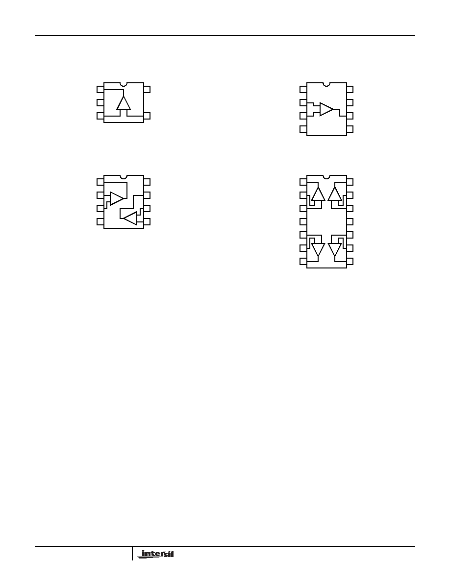
Pinouts
EL9211
(5-PIN SOT-23)
TOP VIEW
EL9211
(8-PIN HMSOP)
TOP VIEW
EL9212
(8-PIN HMSOP)
TOP VIEW
EL9214
(14-PIN HTSSOP)
TOP VIEW
1
2
3
5
4
-
+
OUT
VS-
IN+
VS+
IN-
1
2
3
4
8
7
6
5
-
+
NC
IN-
IN+
NC
OUT
VS+
NC
VS-
1
2
3
4
8
7
6
5
VOUTA
VINA-
VINA+
VS+
VINB-
VOUTB
VINB+
VS-
-
+
-
+
1
2
3
4
14
13
12
11
5
6
7
10
9
8
VOUTA
VINA-
VINA+
VOUTD
VIND+
VIND-
VS-
VS+
VINB+
VINB-
VINC-
VINC+
VOUTC
VOUTB
- +
-
+
- +
-
+
EL9211, EL9212, EL9214
3
FN7007.0
December 22, 2004
IMPORTANT NOTE: All parameters having Min/Max specifications are guaranteed. Typ values are for information purposes only. Unless otherwise noted, all tests are
at the specified temperature and are pulsed tests, therefore: T
J
= T
C
= T
A
Absolute Maximum Ratings
(T
A
= 25°C)
Supply Voltage between V
S
+ and V
S
- . . . . . . . . . . . . . . . . . . . .+15V
Input Voltage . . . . . . . . . . . . . . . . . . . . . . . . . . V
S
- - 0.5V, V
S
+0.5V
Maximum Continuous Output Current . . . . . . . . . . . . . . . . . . 100mA
Ambient Operating Temperature . . . . . . . . . . . . . . . .-40°C to +85°C
Power Dissipation . . . . . . . . . . . . . . . . . . . . . . . . . . . . . See Curves
Maximum Die Temperature . . . . . . . . . . . . . . . . . . . . . . . . . . +125°C
Storage Temperature . . . . . . . . . . . . . . . . . . . . . . . .-65°C to +150°C
CAUTION: Stresses above those listed in "Absolute Maximum Ratings" may cause permanent damage to the device. This is a stress only rating and operation of the
device at these or any other conditions above those indicated in the operational sections of this specification is not implied.
Electrical Specifications
V
S
+ = +6V, V
S
- = -6V, R
L
= 10k
, R
F
= 0
, C
L
= 10pF to 0V, Gain = -1, T
A
= 25°C, unless otherwise specified.
PARAMETER
DESCRIPTION
CONDITIONS
MIN
TYP
MAX
UNIT
INPUT CHARACTERISTICS
V
OS
Input Offset Voltage
V
CM
= 6V
-6
-1
+2
mV
TCV
OS
Average Offset Voltage Drift
(Note)
10
µV/
°C
I
B
Input Bias Current
V
CM
= 6V
-1.4
-0.4
µA
R
IN
Input Impedance
1
G
C
IN
Input Capacitance
1.35
pF
V
REG
Load Regulation
V
COM
= 6V, -100mA < I
L
< 100mA
-20
+20
mV
CMIR
Common Mode Input Range
-0.5
+12.5
V
CMRR
Common Mode Rejection Ratio
For V
IN
from -0.5 to +12.5V
75
100
dB
A
VOL
Open Loop Gain
55
70
dB
OUTPUT CHARACTERISTICS
V
OL
Output Swing Low
I
L
= -5mA
0.9
1.1
V
V
OH
Output Swing High
I
L
= +5mA
10.7
10.94
V
I
SC
Short Circuit Current
300
mA
POWER SUPPLY PERFORMANCE
PSRR
Power Supply Rejection Ratio
V
S
from 4.5V to 10.5V
50
75
dB
I
S
Total Supply Current
EL9211 (no load)
2.3
2.9
mA
EL9212 (no load)
4.5
5
mA
EL9214 (no load)
8.8
9.6
mA
DYNAMIC PERFORMANCE
SR
Slew Rate (Note)
2V step, 20% to 80%
90
115
V/µs
t
S
Settling to +0.1% (A
V
= -1)
(A
V
= -1), V
O
= 2V step
30
ns
BW
-3dB Bandwidth
R
L
= 10k
, C
L
= 10pF, A
V
= +1
130
MHz
R
L
= 10k
, C
L
= 10pF, A
V
= -1
52
MHz
GBWP
Gain-Bandwidth Product
R
L
= 10k
, C
L
= 10pF
63
MHz
PM
Phase Margin
R
L
= 10k
, C
L
= 10pF
43
°
NOTE: Slew rate is measured on rising and falling edges.
EL9211, EL9212, EL9214
4
FN7007.0
December 22, 2004
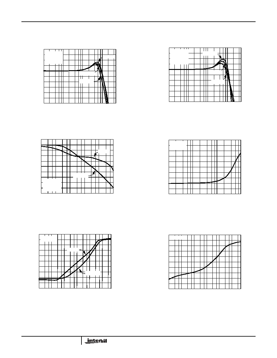
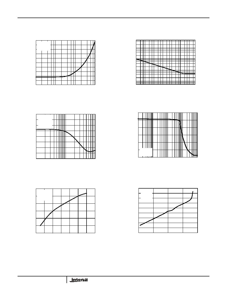
Typical Performance Curves
FIGURE 1. FREQUENCY RESPONSE FOR VARIOUS R
L
FIGURE 2. FREQUENCY RESPONSE FOR VARIOUS C
L
FIGURE 3. OPEN LOOP GAIN AND PHASE vs FREQUENCY
FIGURE 4. CLOSED LOOP OUTPUT IMPEDANCE vs
FREQUENCY
FIGURE 5. PSRR
FIGURE 6. CMRR
GAI
N
(dB)
100K
1M
10M
500M
FREQUENCY (Hz)
100M
V
S
=±6V
A
V
=+1
C
L
=10pF
6
2
-2
-6
-10
8
4
0
-4
-8
-12
R
L
=1k
R
L
=10k
R
L
=100
GAIN (dB)
6
2
-2
-6
-10
8
4
0
-4
-8
100K
1M
10M
500M
FREQUENCY (Hz)
100M
V
S
=±6V
A
V
=+1
R
F
=0
R
L
=10k
-12
C
L
=18pF
C
L
=0pF
C
L
=10pF
10K
100K
100M
FREQUENCY (Hz)
1K
10M
1M
10
20
30
40
50
60
70
80
GA
IN (
d
B)
0
-10
-20
V
S
=±6V
R
L
=10k
C
L
=10pF
PHASE
GAIN
-100
-50
0
50
100
150
200
250
PHASE (°
)
-150
-200
-250
OUTP
UT IM
P
E
DANCE
(
)
70
50
30
10
-10
80
60
40
20
0
100K
1M
10M
FREQUENCY (Hz)
100M
-20
V
S
=±6V
A
V
=+1
10K
100K
100M
FREQUENCY (Hz)
1K
10M
1M
P
S
R
R
(
d
B
)
500M
0
-20
-40
-60
-80
10
-10
-30
-50
-70
-90
PSRR-
PSRR+
V
S
=±6V
CMRR (dB)
-10
-30
-50
-70
-90
-20
-40
-60
-80
1K
100K
10M
FREQUENCY (Hz)
500M
-100
V
S
=±6V
10K
1M
100M
EL9211, EL9212, EL9214
5
FN7007.0
December 22, 2004
FIGURE 7. CHANNEL SEPARATION FOR EL9212/EL9214
FIGURE 8. VOLTAGE NOISE vs FREQUENCY
FIGURE 9. THD + NOISE vs FREQUENCY
FIGURE 10. MAXIMUM OUTPUT SWING vs FREQUENCY
FIGURE 11. SMALL SIGNAL OVERSHOOT vs LOAD
CAPACITANCE
FIGURE 12. V
OUT
- V
S
- vs I
SINK
Typical Performance Curves
(Continued)
CHANNE
L
S
E
P
A
RA
TION
-30
-50
-70
-90
-110
-20
-40
-60
-80
-100
100K
1M
10M
FREQUENCY (Hz)
100M
-120
V
S
=±6V
A
V
=+1
R
L
=10k
1K
100K
100M
FREQUENCY (Hz)
100
10M
1M
10
100
1000
VO
L
T
A
G
E NOI
SE (nV/
Hz)
1
10K
500M
0.022
0.0225
0.023
0.0235
0.024
0.0245
0.025
0.0255
0.026
1K
10K
100K
FREQUENCY (Hz)
THD+N
(%)
V
S
=±6V
A
V
=+1
R
F
=0
V
OPP
=1V
R
L
=50
0
2
4
6
8
10
12
10K
100K
1M
10M
100M
MAX O
U
TPUT S
W
ING
(V
OP-P
)
V
S
=±6V
A
V
=+1
R
L
=10k
FREQUENCY (Hz)
20
30
40
50
60
70
80
0
20
40
60
80
100
120
140
LOAD CAPACITANCE (pF)
OVE
R
S
H
OOT
(%
)
V
S
=±6V
A
V
=+1
R
L
=10k
V
IN
=±50mV
0
0.5
1
1.5
2
2.5
3
3.5
4
4.5
0
0.05
0.1
0.15
0.2
I
SINK
(A)
V
OU
T
-
V
S
- (V)
V
S
=±6V
R
F
=6k
V
IN
+=6V
EL9211, EL9212, EL9214