HIP6017
210
TM
HIP6017
Advanced PWM and Dual Linear Power
Control
The HIP6017 provides the power control and protection for
three output voltages in high-performance microprocessor
and computer applications. The IC integrates a PWM
controller, a linear regulator and a linear controller as well as
the monitoring and protection functions into a single 28 lead
SOIC package. The PWM controller regulates the
microprocessor core voltage with a synchronous-rectified
buck converter. The linear controller regulates power for the
GTL bus and the linear regulator provides power for the
clock driver circuits.
The HIP6017 includes an Intel-compatible, TTL 5-input
digital-to-analog converter (DAC) that adjusts the core PWM
output voltage from 2.1V
DC
to 3.5V
DC
in 0.1V increments
and from 1.8V
DC
to 2.05V
DC
in 0.05V steps. The precision
reference and voltage-mode control provide
�
1% static
regulation. The linear regulator uses an internal pass device
to provide 2.5V
�
2.5%. The linear controller drives an
external N-Channel MOSFET to provide 1.5V
�
2.5%.
The HIP6017 monitors all the output voltages. A single
Power Good signal is issued when the core is within
�
10% of
the DAC setting and the other levels are above their under-
voltage levels. Additional built-in over-voltage protection for
the core output uses the lower MOSFET to prevent output
voltages above 115% of the DAC setting. The PWM over-
current function monitors the output current by using the
voltage drop across the upper MOSFET's r
DS(ON)
, thus
eliminating the need for a current sensing resistor.
Pinout
HIP6017 (SOIC)
TOP VIEW
Features
� Provides 3 Regulated Voltages
- Microprocessor Core, Clock and GTL Power
� Drives N-Channel MOSFETs
� Operates from +3.3V, +5V and +12V Inputs
� Simple Single-Loop PWM Control Design
- Voltage-Mode Control
� Fast Transient Response
- High-Bandwidth Error Amplifier
- Full 0% to 100% Duty Ratios
� Excellent Output Voltage Regulation
- Core PWM Output:
�
1% Over Temperature
- Other Outputs:
�
2.5% Over Temperature
� TTL-Compatible 5-Bit Digital-to-Analog Core Output
Voltage Selection
- Wide Range . . . . . . . . . . . . . . . . . . . 1.8V
DC
to 3.5V
DC
- 0.1V Steps . . . . . . . . . . . . . . . . . . . . 2.1V
DC
to 3.5V
DC
- 0.05V Steps . . . . . . . . . . . . . . . . . . 1.8V
DC
to 2.05V
DC
� Power-Good Output Voltage Monitor
� Microprocessor Core Voltage Protection Against Shorted
MOSFET
� Over-Voltage and Over-Current Fault Monitors
- Does Not Require Extra Current Sensing Element,
Uses MOSFET's r
DS(ON)
� Small Converter Size
- Constant Frequency Operation
- 200kHz Free-Running Oscillator; Programmable from
50kHz to over 1MHz
Applications
� Full Motherboard Power Regulation for Computers
� Low-Voltage Distributed Power Supplies
NC
NC
VID4
VID3
V33
NC
SS
FAULT/RT
FB2
VCC
PGND
LGATE1
PHASE1
GATE3
COMP1
GND
VOUT2
VIN2
UGATE1
28
27
26
25
24
23
22
21
20
19
18
17
16
15
1
2
3
4
5
6
7
8
9
10
11
12
13
14
PGOOD
VID2
GND2
VSEN1
FB3
VID1
VID0
OCSET1
FB1
Ordering Information
PART NUMBER
TEMP. RANGE
(
o
C)
PACKAGE
PKG. NO.
HIP6017CB
0 to 70
28 Ld SOIC
M28.3
HIP6017EVAL1
Evaluation Board
Data Sheet
April 1999
FN4496.1
CAUTION: These devices are sensitive to electrostatic discharge; follow proper IC Handling Procedures.
1-888-INTERSIL or 321-724-7143
|
Intersil (and design) is a trademark of Intersil Americas Inc.
Copyright � Intersil Americas Inc. 2002. All Rights Reserved
2-
211
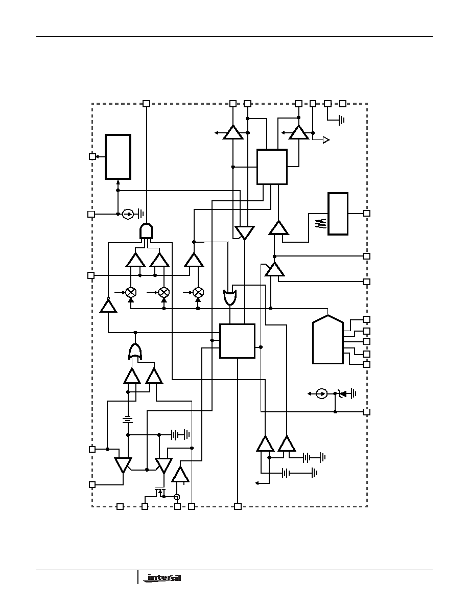
Block Diagram
0.23A
115%
110%
90%
INHIBIT
PWM
COMP
ERROR
AMP
VCC
PGOOD
PWM
GND
VSEN1
OCSET1
VID0
VID1
VID2
VID3
FB1
COMP1
DACOUT
UGATE1
PHASE1
200
�
A
11
�
A
4V
+
-
+
-
+
-
+
-
VID4
LGATE1
PGND
VOUT2
GATE3
FB3
INHIBIT
RT
0.3V
+
-
+
-
+
-
+
-
1.26V
+
-
POWER-ON
RESET (POR)
OSCILLATOR
+
-
GATE
CONTROL
VCC
VCC
VCC
SS
LOWER
DRIVE
UPPER
+
-
+
-
UNDER-
VOLTAGE
FB2
LINEAR
OV
LUV
OC1
OC2
+
-
TTL D/A
CONVERTER
(DAC)
VIN2
FAULT
SOFT-
START
& FAULT
LOGIC
DRIVE
V33
+
-
+
2.5V
-
4.3V
+
-
+
VIN2
FIGURE 1.
GND2
H
I
P
601
7
212
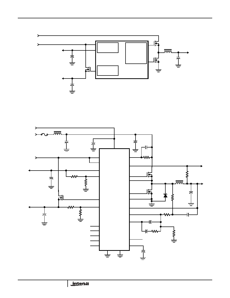
Simplified Power System Diagram
Typical Application
PWM1
+5V
IN
V
OUT1
V
OUT2
V
OUT3
LINEAR
LINEAR
HIP6017
REGULATOR
CONTROLLER
CONTROLLER
+3.3V
IN
FIGURE 2.
+3.3V
IN
VID1
VID2
VID3
VID4
SS
GND2
VCC
+5V
IN
VID0
+12V
IN
V
OUT1
PGND
VSEN1
PGOOD
LGATE1
UGATE1
OCSET1
PHASE1
Q1
Q2
POWERGOOD
FB1
COMP1
1.8V TO 3.5V
DRIVE3
FB3
VOUT2
C
OUT2
1.5V
2.5V
C
OUT3
C
IN
C
OUT1
Q3
CR1
L
OUT1
HIP6017
V
OUT3
V
OUT2
FAULT/RT
FB2
C
SS
VIN2
V33
GND
L
IN
FIGURE 3.
HIP6017
213
Absolute Maximum Ratings
Thermal Information
Supply Voltage, V
CC
. . . . . . . . . . . . . . . . . . . . . . . . . . . . . . . . .+15V
PGOOD, RT, FAULT, and GATE Voltage . . GND - 0.3V to V
CC
+ 0.3V
Input, Output or I/O Voltage. . . . . . . . . . . . . . . . . . GND -0.3V to 7V
Operating Conditions
Supply Voltage, V
CC
. . . . . . . . . . . . . . . . . . . . . . . . . . . +12V
�
10%
Ambient Temperature Range. . . . . . . . . . . . . . . . . . . . . 0
o
C to 70
o
C
Junction Temperature Range . . . . . . . . . . . . . . . . . . . 0
o
C to 125
o
C
Thermal Resistance (Typical, Note 1)
JA
(
o
C/W)
SOIC Package . . . . . . . . . . . . . . . . . . . . . . . . . . . .
60
SOIC Package (with 3 in
2
of copper) . . . . . . . . . . .
50
Maximum Junction Temperature (Plastic Package) . . . . . . . .150
o
C
Maximum Storage Temperature Range . . . . . . . . . -65
o
C to 150
o
C
Maximum Lead Temperature (Soldering 10s) . . . . . . . . . . . . . 300
o
C
(SOIC - Lead Tips Only)
CAUTION: Stresses above those listed in "Absolute Maximum Ratings" may cause permanent damage to the device. This is a stress only rating and operation of the
device at these or any other conditions above those indicated in the operational sections of this specification is not implied.
NOTE:
1.
JA
is measured with the component mounted on an evaluation PC board in free air.
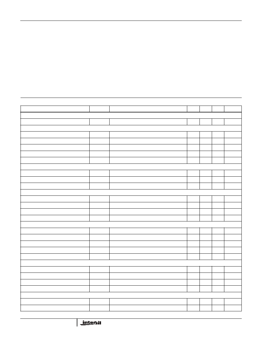
Electrical Specifications
Recommended Operating Conditions, Unless Otherwise Noted. Refer to Figures 1, 2 and 3
PARAMETER
SYMBOL
TEST CONDITIONS
MIN
TYP
MAX
UNITS
VCC SUPPLY CURRENT
Nominal Supply
I
CC
UGATE1, DRIVE3, LGATE1, and VOUT4 Open
-
10
-
mA
POWER-ON RESET
Rising VCC Threshold
V
OCSET
= 4.5V
8.6
-
10.4
V
Falling VCC Threshold
V
OCSET
= 4.5V
8.2
-
10.2
V
Rising VIN2 Under-Voltage Threshold
2.45
2.55
2.65
V
VIN2 Under-Voltage Hystersis
-
500
-
mV
Rising V
OCSET1
Threshold
-
1.25
-
V
OSCILLATOR
Free Running Frequency
RT = OPEN
185
200
215
kHz
Total Variation
6k
< RT to GND < 200k
-15
-
+15
%
Ramp Amplitude
V
OSC
RT = Open
-
1.9
-
V
P-P
REFERENCE AND DAC
DAC(VID0-VID4) Input Low Voltage
-
-
0.8
V
DAC(VID0-VID4) Input High Voltage
2.0
-
-
V
DACOUT Voltage Accuracy
-1.0
-
+1.0
%
Reference Voltage (Pin FB2 and FB3)
1.240
1.265 1.290
V
LINEAR REGULATOR
Regulation
10mA < I
VOUT2
< 150mA
-2.5
-
+2.5
%
Under Voltage Level
FB2
UV
FB2 Rising
-
75
87
%
Under Voltage Hysteresis
-
6
-
%
Over Current Protection
180
230
-
mA
Over Current Protection During Start-Up
560
700
-
mA
LINEAR CONTROLLER
Regulation
VSEN3 = DRIVE3, 0 < I
DRIVE3
< 20mA
-2.5
-
+2.5
%
Under Voltage Level
FB3
UV
FB3 Rising
-
75
87
%
Under Voltage Hysteresis
-
6
-
%
Output Drive Current
I
DRIVE3
VIN2 - V
DRIVE3
> 0.6V
20
40
-
mA
PWM CONTROLLER ERROR AMPLIFIER
DC Gain
-
88
-
dB
Gain-Bandwidth Product
GBWP
-
15
-
MHz
HIP6017
214
Functional Pin Descriptions
VSEN1 (Pin 22)
This pin is connected to the PWM converter's output voltage.
The PGOOD and OVP comparator circuits use this signal to
report output voltage status and for over-voltage protection.
OCSET1 (Pin 23)
Connect a resistor (R
OCSET
) from this pin to the drain of the
respective upper MOSFET. R
OCSET
, an internal 200
�
A
current source (I
OCSET
), and the upper MOSFET on-
resistance (r
DS(ON)
) set the converter over-current (OC) trip
point according to the following equation:
An over-current trip cycles the soft-start function. Sustaining
an over-current for 2 soft-start intervals shuts down the IC.
Additionally, OCSET1 is an output for the inverted FAULT
signal (FAULT). If a fault condition causes FAULT to go high,
OCSET1 will be simultaneously pulled to ground though an
internal MOS device (typical r
DS(ON)
= 100
).
Slew Rate
SR
COMP = 10pF
-
6
-
V/
�
s
PWM CONTROLLER GATE DRIVER
Upper Drive Source
I
UGATE
VCC = 12V, V
UGATE1
= 6V
-
1
-
A
Upper Drive Sink
R
UGATE
V
UGATE1-PHASE1
= 1V
-
1.7
3.5
Lower Drive Source
I
LGATE
VCC = 12V, V
LGATE1
= 1V
-
1
-
A
Lower Drive Sink
R
LGATE
V
LGATE1
= 1V
-
1.4
3.0
PROTECTION
V
OUT1
Over-Voltage Trip
VSEN1 Rising
112
115
118
%
FAULT Sourcing Current
I
OVP
V
FAULT/RT
= 10V
10
14
-
mA
OCSET1 Current Source
I
OCSET
V
OCSET
= 4.5V
DC
170
200
230
�
A
Soft-Start Current
I
SS
-
11
-
�
A
Chip Shutdown Soft-Start Threshold
-
-
1.0
V
POWER GOOD
V
OUT1
Upper Threshold
VSEN1 Rising
108
-
110
%
V
OUT1
Under-Voltage (Lower Threshold)
VSEN1 Rising
92
-
94
%
V
OUT1
Hysteresis (VSEN1/DACOUT)
Upper/Lower Threshold
-
2
-
%
PGOOD Voltage Low
V
PGOOD
I
PGOOD
= -4mA
-
-
0.5
V
Electrical Specifications
Recommended Operating Conditions, Unless Otherwise Noted. Refer to Figures 1, 2 and 3 (Continued)
PARAMETER
SYMBOL
TEST CONDITIONS
MIN
TYP
MAX
UNITS
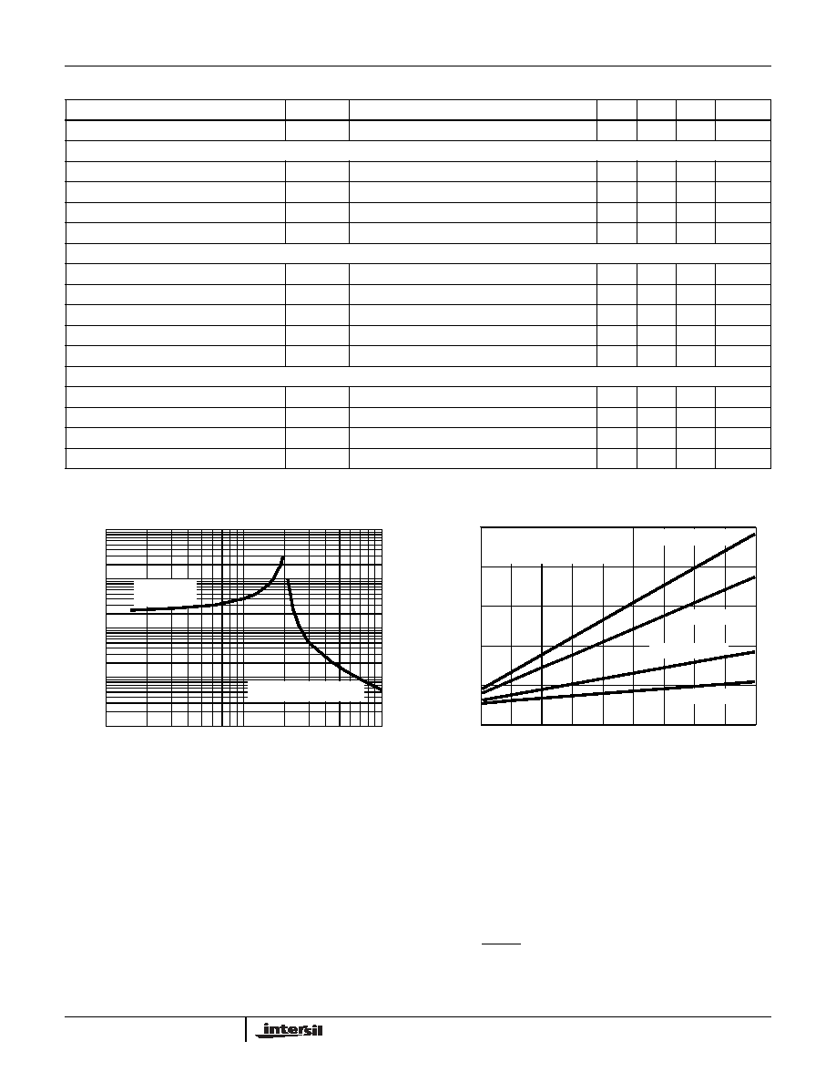
Typical Performance Curves
FIGURE 4. R
T
RESISTANCE vs FREQUENCY
FIGURE 5. BIAS SUPPLY CURRENT vs FREQUENCY
10
100
1000
SWITCHING FREQUENCY (kHz)
RE
S
I
S
T
ANCE
(
k
)
10
100
1000
R
T
PULLUP
TO +12V
R
T
PULLDOWN TO V
SS
100 200
300
400
500
600
700
800
900 1000
0
20
40
60
80
100
SWITCHING FREQUENCY (kHz)
I
CC
(m
A
)
C
UGATE1
= C
LGATE1
= C
GATE
C
GATE
= 4800pF
C
GATE
= 3600pF
C
GATE
= 1500pF
C
GATE
= 660pF
V
VCC
= 12V, V
IN
= 5V
I
PEAK
I
OCSET
xR
OCSET
r
DS ON
(
)
-------------------------------------------------
=
HIP6017