1
TM
HIP6502B
Multiple Linear Power Controller with
ACPI Control Interface
The HIP6502B complements either an HIP6020 or an
HIP6021 in ACPI-compliant designs for microprocessor and
computer applications. The IC integrates four linear
controllers/regulators, switching, monitoring and control
functions into a 20-pin SOIC package. One linear controller
generates the 3.3V
DUAL
/3.3V
SB
voltage plane from the ATX
supply's 5VSB output, powering the south bridge and the
PCI slots through an external pass transistor during sleep
states (S3, S4/S5). A second transistor is used to switch in
the ATX 3.3V output for operation during S0 and S1/S2
(active) operating states. Two linear controllers/regulators
supply at choice either or both of the computer system's
2.5V or 3.3V memory power through external pass
transistors in active states. During sleep states, integrated
pass transistors supply the sleep power. Another controller
powers up the 5V
DUAL
plane by switching in the ATX 5V
output in active states, and the ATX 5VSB in sleep states.
One internal regulator outputs a dedicated, noise-free 2.5V
clock chip supply. The HIP6502B's operating mode (active
outputs or sleep outputs) is selectable through two digital
control pins, S3 and S5. Enabling sleep state support on the
5V
DUAL
output is offered through the EN5VDL pin. In active
state, the 3.3V
DUAL
and 3.3V
MEM
linear regulators use
external N-channel pass MOSFETs to connect the outputs
directly to the 3.3V input supplied by an ATX (or equivalent)
power supply, for minimal losses. In sleep state, power
delivery on both outputs is transferred to NPN transistors -
external to the controller on the 3.3V
DUAL
, internal on the
3.3V
MEM
. Active state regulation on the 2.5V
MEM
output is
performed through an external NPN transistor. In sleep
state, conduction on this output is transferred to an internal
pass transistor. The 5V
DUAL
output is powered through two
external MOS transistors. In sleep states, a PMOS (or PNP)
transistor conducts the current from the ATX 5VSB output;
while in active state, current flow is transferred to an NMOS
transistor connected to the ATX 5V output. The operation of
the 5V
DUAL
output is dictated not only by the status of the
S3 and S5 pins, but that of the EN5VDL pin as well. The
3.3V
DUAL
/3.3V
SB
output is active for as long as the ATX
5VSB voltage is applied to the chip. The 2.5V
CLK
output is
only active during S0 and S1/S2, and uses the 3V3 pin as
input source for its internal pass element.
Features
� Provides 5 ACPI-Controlled Voltages
- 5V
DUAL
USB/Keyboard/Mouse (Active/Sleep)
- 3.3V
DUAL
/3.3V
SB
PCI/Auxiliary/LAN (Active/Sleep)
- 2.5V
MEM
RDRAM (Active/Sleep)
- 3.3V
MEM
SDRAM (Active/Sleep)
- 2.5V
CLK
Clock/Processor Terminations (Active Only)
� Excellent Output Voltage Regulation
- 3.3V
DUAL
/3.3V
SB
Output:
�
2.0% Over Temperature;
Sleep State Only
- 2.5V
MEM
and 3.3V
MEM
Output:
�
2.0% Over
Temperature; Both Operational States (3.3V
MEM
in
Sleep Only)
- 2.5V
CLK
Output:
�
2.0% Over Temperature
� Small Size
- Very Low External Component Count
� Dual Memory Voltage Support Via MSEL Pin
- 2.5V for RDRAM Memory
- 3.3V for SDRAM Memory
- Both 2.5V and 3.3V for Flexible Systems
� Under-Voltage Monitoring of All Outputs with Centralized
FAULT Reporting and Temperature Shutdown
Applications
� Motherboard Power Regulation for ACPI-Compliant
Computers
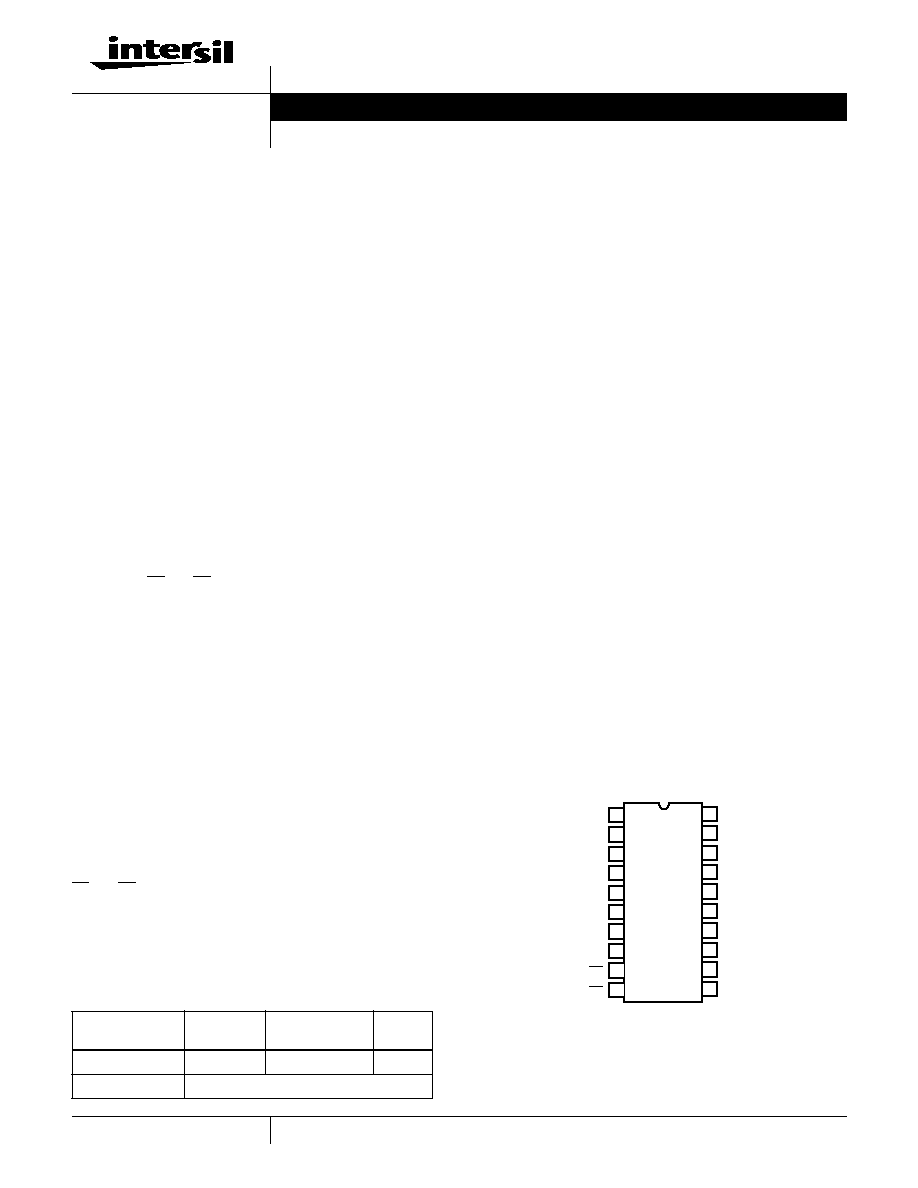
Pinout
HIP6502B
(SOIC)
TOP VIEW
Ordering Information
PART NUMBER
TEMP.
RANGE (
o
C)
PACKAGE
PKG.
NO.
HIP6502BCB
0 to 70
20 Ld SOIC
M20.3
HIP6502BEVAL1
Evaluation Board
14
15
16
17
18
19
20
7
6
5
4
3
2
1
5VSB
VSEN1
VCLK
3V3DLSB
3V3DL
VSEN2
MSEL
5V
5VDLSB
12V
DLA
SS
3V3
DRV2
EN5VDL
5VDL
13
8
11
12
10
9
S3
S5
FAULT
GND
Data Sheet
May 2000
File Number
4871
CAUTION: These devices are sensitive to electrostatic discharge; follow proper IC Handling Procedures.
1-888-INTERSIL or 321-724-7143
|
Intersil and Design is a trademark of Intersil Corporation.
|
Copyright
�
Intersil Corporation 2000
2
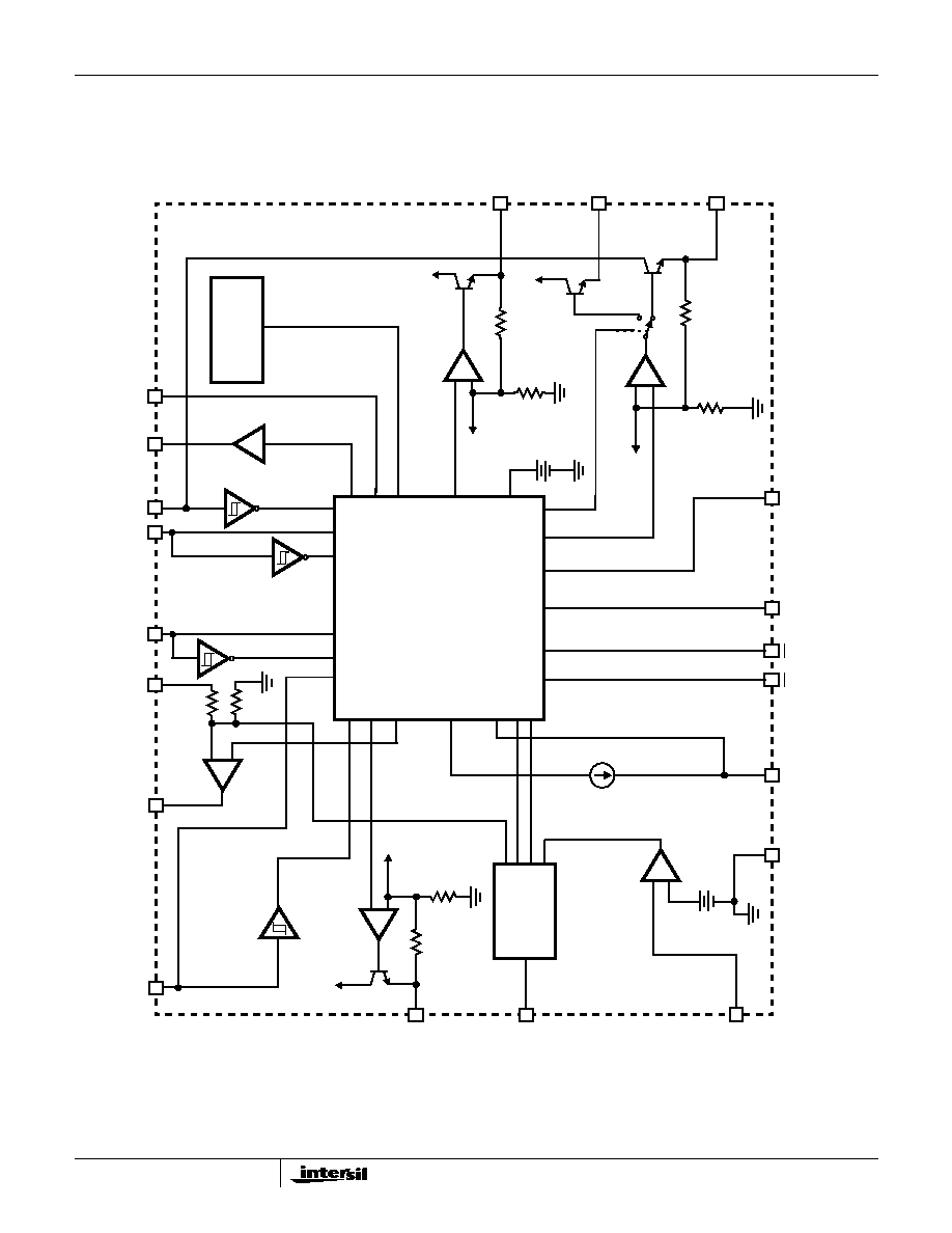
Block Diagram
S5
5VSB
+
-
GND
4.4V/3.2V
EA2
5VSB POR
SS
12V
5VDLSB
+
-
3V3DL
FAULT
UV DETECTOR
TO UV
DETECTOR
MSEL
5VDL
EA4
3V3DLSB
+
-
UV COMPARATOR
3.75V
DLA
VSEN2
DRV2
VSEN1
MONITOR AND CONTROL
10.8V/9.8V
12V MONITOR
+
-
1.265V
TEMPERATURE
MONITOR
(TMON)
+
-
TO
VCLK
TO 3V3
UV DETECTOR
EA3
+
-
TO UV
TO 5VSB
DETECTOR
EA3
S3
EN5VDL
+
-
3V3
5V
10
�
A
TO 5V
FIGURE 1.
3V3 MONITOR
2.97V/2.8V
5V MONITOR
4.5V/4.25V
HIP6502B

3
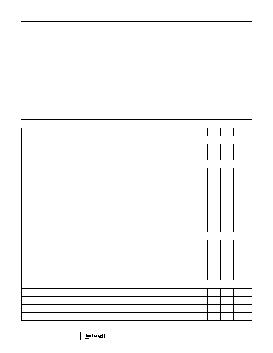
Simplified Power System Diagram
Typical Application
+5V
SB
Q3
2.5V
MEM
LINEAR
HIP6502B
CONTROLLER
+3.3V
IN
+12V
IN
SX
EN5VDL
+5V
IN
3.3V
DUAL
/3.3V
SB
5V
DUAL
CONTROL
LOGIC
Q1
Q4
Q5
Q2
LINEAR
CONTROLLER
FAULT
SHUTDOWN
V
CLK
LINEAR
REGULATOR
LINEAR
REGULATOR
2.5V
3.3V
5V
2
MSEL
Q6
3.3V
MEM
FIGURE 2.
3.3V
2.5V
GND
5VSB
+3.3V
IN
+5V
SB
VSEN2
DRV2
VSEN1
C
OUT2
12V
+12V
IN
V
OUT2
2.5V
MEM
Q1
SLP_S3
S3
V
OUT3
3.3V
DUAL
/3.3V
SB
C
OUT3
+5V
IN
C
OUT5
V
OUT5
5V
DUAL
3V3DL
3V3DLSB
Q2
Q3
Q4
Q5
DLA
5VDLSB
FAULT
5VDL
SS
VCLK
MSEL
EN5VDL
SHUTDOWN
FAULT
V
OUT1
3.3V
MEM
V
OUT4
2.5V
CLK
C
OUT1
C
OUT4
SLP_S5
EN5VDL
S5
MSEL
C
SS
3V3
5V
Q6
FIGURE 3.
HIP6502B
HIP6502B
4
Absolute Maximum Ratings
Thermal Information
Supply Voltage, V
5VSB
. . . . . . . . . . . . . . . . . . . . . . . . . . . . . . +7.0V
12V. . . . . . . . . . . . . . . . . . . . . . . . . . . . . . . . . GND - 0.3V to +14.5V
DLA, DRV2. . . . . . . . . . . . . . . . . . . . . . . .GND - 0.3V to V
12V
+0.3V
All Other Pins . . . . . . . . . . . . . . . . . . . . .GND - 0.3V to 5VSB + 0.3V
ESD Classification . . . . . . . . . . . . . . . . . . . . . . . . . . . . . . . . . Class 3
Recommended Operating Conditions
Supply Voltage, V
5VSB
. . . . . . . . . . . . . . . . . . . . . . . . . . . +5V
�
5%
Lowest 5VSB Supply Voltage Guaranteeing Parameters . . . . +4.5V
Digital Inputs, V
SX
, V
EN5VDL
, V
MSEL
. . . . . . . . . . . . . . . 0 to +5.5V
Ambient Temperature Range . . . . . . . . . . . . . . . . . . . . . 0
o
C to 70
o
C
Junction Temperature Range . . . . . . . . . . . . . . . . . . . . 0
o
C to 125
o
C
Thermal Resistance (Typical, Note 1)
JA
(
o
C/W)
SOIC Package. . . . . . . . . . . . . . . . . . . . . . . . . . . . .
87
Maximum Junction Temperature (Plastic Package) . . . . . . . .150
o
C
Maximum Storage Temperature Range . . . . . . . . . . -65
o
C to 150
o
C
Maximum Lead Temperature (Soldering 10s) . . . . . . . . . . . . .300
o
C
(SOIC - Lead Tips Only)
CAUTION: Stresses above those listed in "Absolute Maximum Ratings" may cause permanent damage to the device. This is a stress only rating and operation of the
device at these or any other conditions above those indicated in the operational sections of this specification is not implied.
NOTE:
1.
JA
is measured with the component mounted on a low effective thermal conductivity test board in free air. See Tech Brief TB379 for details.
Electrical Specifications
Recommended Operating Conditions, Unless Otherwise Noted Refer to Figures 1, 2 and 3
PARAMETER
SYMBOL
TEST CONDITIONS
MIN
TYP
MAX
UNITS
VCC SUPPLY CURRENT
Nominal Supply Current
I
5VSB
-
30
-
mA
Shutdown Supply Current
I
5VSB(OFF)
V
SS
= 0.8V
-
14
-
mA
POWER-ON RESET, SOFT-START, AND VOLTAGE MONITORS
Rising 5VSB POR Threshold
-
-
4.5
V
5VSB POR Hysteresis
-
1.0
-
V
Rising 12V Threshold
-
-
10.8
V
12V Hysteresis
-
1.0
-
V
Rising 3V3 and 5V Thresholds
-
90
-
%
3V3 and 5V Hysteresis
-
5
-
%
Soft-Start Current
I
SS
-
10
-
�
A
Shutdown Voltage Threshold
V
SD
-
-
0.8
V
3.3V
MEM
LINEAR REGULATOR (V
OUT1
)
Sleep State Regulation
-
-
2.0
%
VSEN1 Nominal Voltage Level
V
VSEN1
MSEL > 1.8V
-
3.3
-
V
VSEN1 Undervoltage Rising Threshold
-
2.739
-
V
VSEN1 Undervoltage Hysteresis
-
99
-
mV
VSEN1 Output Current
I
VSEN1
5VSB = 5V
250
300
-
mA
2.5V
MEM
LINEAR REGULATOR (V
OUT2
)
Regulation
-
-
2.0
%
VSEN2 Nominal Voltage Level
V
VSEN2
MSEL < 2.0V
-
2.5
-
V
VSEN2 Undervoltage Rising Threshold
-
2.075
-
V
VSEN2 Output Current
I
VSEN2
5VSB = 5V
250
300
-
mA
HIP6502B
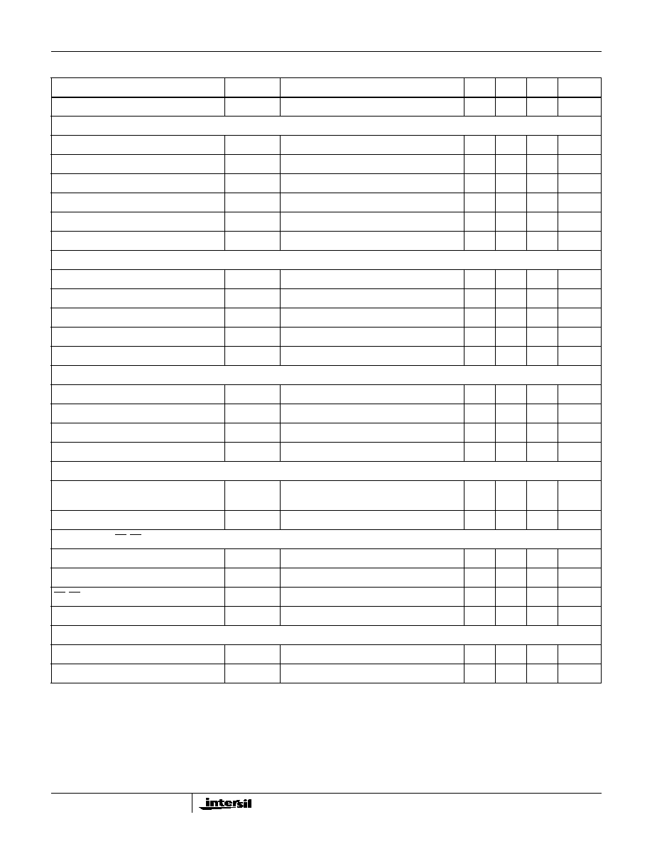
5
DRV2 Output Drive Current
I
DRV2
5VSB = 5V
220
-
-
mA
3.3V
DUAL
/3.3V
SB
LINEAR REGULATOR (V
OUT3
)
Sleep State Regulation
-
-
2.0
%
3V3DL Nominal Voltage Level
V
3V3DL
-
3.3
-
V
3V3DL Undervoltage Rising Threshold
-
2.739
-
V
3V3DL Undervoltage Hysteresis
-
99
-
mV
3V3DLSB Output Drive Current
I
3V3DLSB
5VSB = 5V
5
10
-
mA
DLA Output Impedance
-
90
-
2.5V
CLK
LINEAR REGULATOR (V
OUT4
)
Regulation
-
-
2.0
%
VCLK Nominal Voltage Level
V
VCLK
-
2.5
-
V
VCLK Undervoltage Rising Threshold
-
2.075
-
V
VCLK Undervoltage Hysteresis
-
75
-
mV
VCLK Output Current (Note 2)
I
VCLK
V
3V3
= 3.3V
500
800
-
mA
5V
DUAL
SWITCH CONTROLLER (V
OUT5
)
5VDL Undervoltage Rising Threshold
-
4.150
-
V
5VDL Undervoltage Hysteresis
-
150
-
mV
5VDLSB Output Drive Current
I
5VDLSB
5VDLSB = 4V, 5VSB = 5V
-20
-
-40
mA
5VDLSB Pull-Up Impedance to 5VSB
-
350
-
TIMING INTERVALS
Active State Assessment Past Input UV
Thresholds (Note 3)
20
25
30
ms
Active-to-Sleep Control Input Delay
-
200
-
�
s
CONTROL I/O (S3, S5, EN5VDL, MSEL, FAULT)
High Level Input Threshold
-
-
2.2
V
Low Level Input Threshold
0.8
-
-
V
S3, S5 Internal Pull-up Impedance to 5VSB
-
50
-
k
FAULT Output Impedance
FAULT = high
-
100
-
TEMPERATURE MONITOR
Fault-Level Threshold (Note 4)
125
-
-
o
C
Shutdown-Level Threshold (Note 4)
-
155
-
o
C
NOTES:
2. At Ambient Temperatures Less Than 50
o
C.
3. Guaranteed by Correlation.
4. Guaranteed by Design.
Electrical Specifications
Recommended Operating Conditions, Unless Otherwise Noted Refer to Figures 1, 2 and 3 (Continued)
PARAMETER
SYMBOL
TEST CONDITIONS
MIN
TYP
MAX
UNITS
HIP6502B