 | ÐлекÑÑоннÑй компоненÑ: FN6094 | СкаÑаÑÑ:  PDF PDF  ZIP ZIP |
Äîêóìåíòàöèÿ è îïèñàíèÿ www.docs.chipfind.ru
1
®
FN6094.3
ISL83699
Ultra Low ON-Resistance, Low Voltage,
Single Supply, Quad SPDT (Dual DPDT)
Analog Switch
The Intersil ISL83699 device is a low ON-resistance, low
voltage, bidirectional, Quad SPDT (Dual DPDT) analog
switch designed to operate from a single +1.65V to +3.6V
supply. Targeted applications include battery powered
equipment that benefit from low on-resistance (0.26
), and
fast switching speeds (t
ON
= 10ns, t
OFF
= 7ns). The digital
logic input is 1.8V logic-compatible when using a single +3V
supply.
Cell phones, for example, often face ASIC functionality
limitations. The number of analog input or GPIO pins may be
limited and digital geometries are not well suited to analog
switch performance. This family of parts may be used to
"mux-in" additional functionality while reducing ASIC design
risk. The ISL83699 is offered in small form factor packages,
alleviating board space limitations.
The ISL83699 consists of four SPDT switches. It is configured
as a dual double-pole/double-throw (DPDT) device with two
logic control inputs that control two SPDT switches each. The
configuration can be used as a dual differential 2-to-1
multiplexer/demultiplexer. The ISL83699 is pin compatible
with the STG3699.
Related Literature
· Technical Brief TB363 "Guidelines for Handling and
Processing Moisture Sensitive Surface Mount Devices
(SMDs)"
· Application Note AN557 "Recommended Test Procedures
for Analog Switches"
Features
·
Pb-Free Available as an Option (RoHS Compliant)
(see Ordering Info)
· Drop in Replacement for the STG3699
· ON Resistance (R
ON
)
- V+ = +3.0V . . . . . . . . . . . . . . . . . . . . . . . . . . . . . 0.26
- V+ = +1.8V . . . . . . . . . . . . . . . . . . . . . . . . . . . . . 0.45
· R
ON
Matching between Channels . . . . . . . . . . . . . . . .0.04
· R
ON
Flatness Across Signal Range . . . . . . . . . . . . . . .0.06
· Single Supply Operation. . . . . . . . . . . . . . . . +1.65V to +3.6V
· Low Power Consumption (PD). . . . . . . . . . . . . . . . . . <0.2µW
· Fast Switching Action
- t
ON
. . . . . . . . . . . . . . . . . . . . . . . . . . . . . . . . . . . . 10ns
- t
OFF
. . . . . . . . . . . . . . . . . . . . . . . . . . . . . . . . . . . . 7ns
· Guaranteed Break-Before-Make
· 1.8V Logic Compatible (+3V supply)
· Available in 16 lead 3x3 QFN and 16 lead TSSOP
· ESD HBM Rating
- COM Pins . . . . . . . . . . . . . . . . . . . . . . . . . . . . . . . . 9kV
- All Other Pins . . . . . . . . . . . . . . . . . . . . . . . . . . . . . 4kV
Applications
· Battery Powered, Handheld, and Portable Equipment
- Cellular/Mobile Phones
- Pagers
- Laptops, Notebooks, Palmtops
· Portable Test and Measurement
· Medical Equipment
· Audio and Video Switching
TABLE 1. FEATURES AT A GLANCE
ISL83699
Number of Switches
4
SW
Quad SPDT (Dual DPDT)
3.0V R
ON
0.26
3.0V t
ON
/t
OFF
10ns/7ns
1.8V R
ON
0.45
1.8V t
ON
/t
OFF
18ns/10ns
Packages
16 Ld 3x3 QFN, 16 Ld TSSOP
Data Sheet
November 5, 2004
CAUTION: These devices are sensitive to electrostatic discharge; follow proper IC Handling Procedures.
1-888-INTERSIL or 321-724-7143
|
Intersil (and design) is a registered trademark of Intersil Americas Inc.
Copyright Intersil Americas Inc. 2004. All Rights Reserved
All other trademarks mentioned are the property of their respective owners.
2
FN6094.3
November 5, 2004
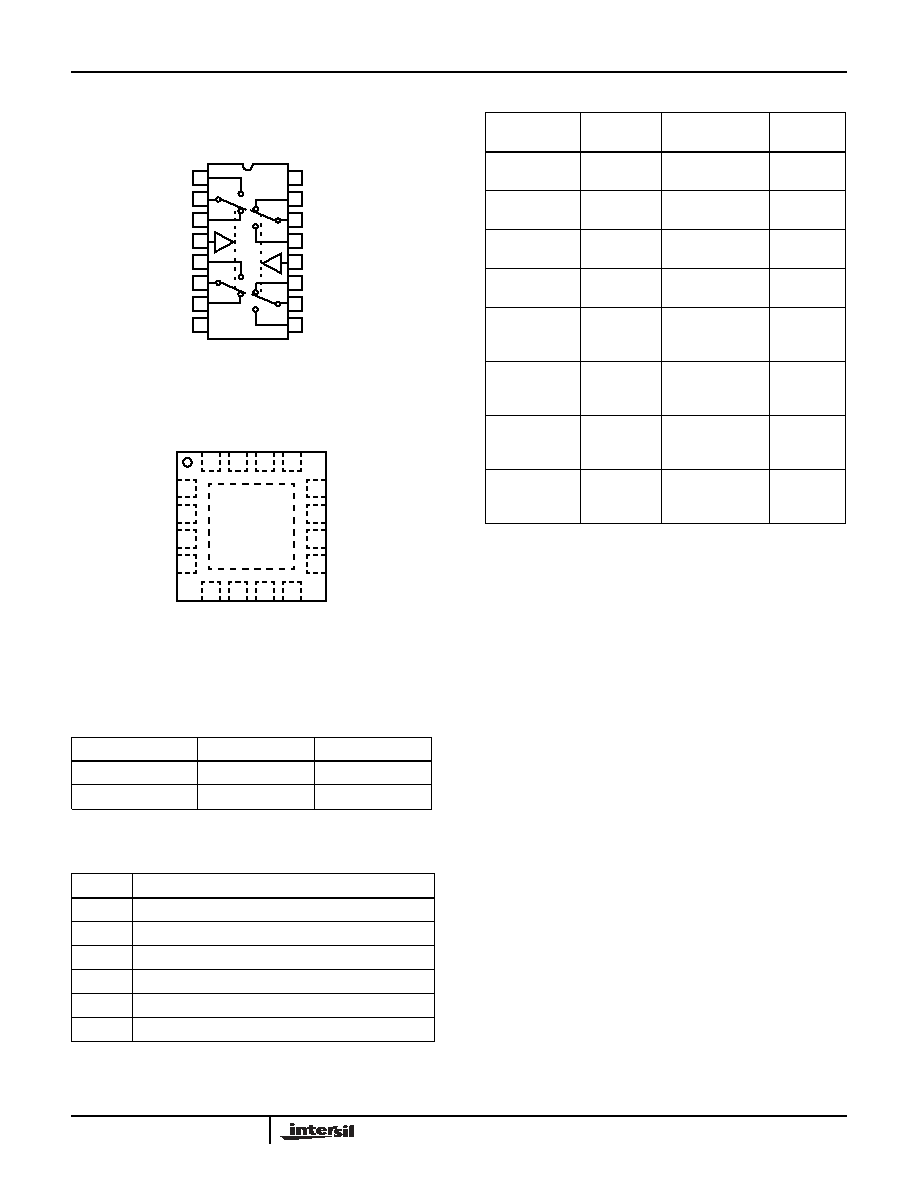
Pinouts
(Note 1)
ISL83699 (TSSOP)
TOP VIEW
ISL83699 (3x3 QFN)
TOP VIEW
NOTE:
1. Switches Shown for Logic "0" Input.
Truth Table
LOGIC
NC SW
NO SW
0
ON
OFF
1
OFF
ON
NOTE: Logic "0"
0.5V. Logic "1"
1.4V with a 3V supply.
Pin Descriptions
PIN
FUNCTION
V+
System Power Supply Input (+1.65V to +3.6V)
GND
Ground Connection
IN
Digital Control Input
COM
Analog Switch Common Pin
NO
Analog Switch Normally Open Pin
NC
Analog Switch Normally Closed Pin
14
15
16
9
13
12
11
10
1
2
3
4
5
7
6
8
NO1
COM1
NC1
IN1-2
NO2
COM2
GND
NC2
V+
COM4
NO4
IN3-4
NC3
COM3
NO3
NC4
NC1
IN1-2
NO2
COM2
CO
M
1
NO
1
V+
NC
4
COM4
NO4
IN3-4
NC3
NC2
GND
NO3
COM3
1
3
4
15
16
14
13
2
12
10
9
11
6
5
7
8
Ordering Information
PART NO.
(BRAND)
TEMP.
RANGE (°C)
PACKAGE
PKG.
DWG. #
ISL83699IR
(83699IR)
-40 to 85
16 Ld 3x3 QFN
L16.3x3
ISL83699IR-T
(83699IR)
-40 to 85
16 Ld 3x3 QFN
Tape and Reel
L16.3x3
ISL83699IV
(83699IV)
-40 to 85
16 Ld TSSO
P
M16.173
ISL83699IV-T
(83699IV)
-40 to 85
16 Ld TSSOP
Tape and Reel
M16.173
ISL83699IRZ
(83699IR)
(See Note)
-40 to 85
16 Ld 3x3 QFN
(Pb-free)
L16.3x3
ISL83699IRZ-T
(83699IR)
(See Note)
-40 to 85
1
6 Ld 3x3 QFN
Tape and Reel
(Pb-free)
L16.3x3
ISL83699IVZ
(83699IV)
(See Note)
-40 to 85
16 Ld TSSO
P
(Pb-free)
M16.173
ISL83699IVZ-T
(83699IV)
(See Note)
-40 to 85
16 Ld TSSO
P
Tape and Reel
(Pb-free)
M16.173
NOTE: Intersil Pb-free products employ special Pb-free material sets;
molding compounds/die attach materials and 100% matte tin plate
termination finish, which are RoHS compliant and compatible with
both SnPb and Pb-free soldering operations. Intersil Pb-free products
are MSL classified at Pb-free peak reflow temperatures that meet or
exceed the Pb-free requirements of IPC/JEDEC J STD-020C.
ISL83699
3
FN6094.3
November 5, 2004
Absolute Maximum Ratings
Thermal Information
V+ to GND . . . . . . . . . . . . . . . . . . . . . . . . . . . . . . . . . . . -0.3 to 4.7V
Input Voltages
NO, NC, IN (Note 2) . . . . . . . . . . . . . . . . . . . -0.3 to ((V+) + 0.3V)
Output Voltages
COM (Note 2) . . . . . . . . . . . . . . . . . . . . . . . . -0.3 to ((V+) + 0.3V)
Continuous Current NO, NC, or COM . . . . . . . . . . . . . . . . .
±
300mA
Peak Current NO, NC, or COM
(Pulsed 1ms, 10% Duty Cycle, Max) . . . . . . . . . . . . . . . .
±
500mA
ESD Rating:
HBM COM
X
. . . . . . . . . . . . . . . . . . . . . . . . . . . . . . . . . . . . . .>9kV
HBM NO
X
, NC
X
, IN
X
, V+, GND . . . . . . . . . . . . . . . . . . . . . . .>4kV
MM COM
X
. . . . . . . . . . . . . . . . . . . . . . . . . . . . . . . . . . . . . .>500V
MM NO
X
, NC
X
, IN
X
, V+, GND . . . . . . . . . . . . . . . . . . . . . . .>300V
CDM . . . . . . . . . . . . . . . . . . . . . . . . . . . . . . . . . . . . . . . . . .>1000V
Thermal Resistance (Typical, Note 3)
JA
(°C/W)
16 Ld 3x3 QFN Package . . . . . . . . . . . . . . . . . . . . .
75
16 Ld TSSOP Package . . . . . . . . . . . . . . . . . . . . . .
150
Maximum Junction Temperature (Plastic Package) . . . . . . . 150°C
Maximum Storage Temperature Range. . . . . . . . . . . . . -65°C to 150°C
Maximum Lead Temperature (Soldering 10s) . . . . . . . . . . . . 300°C
(Lead Tips Only)
Operating Conditions
Temperature Range
ISL83699IX . . . . . . . . . . . . . . . . . . . . . . . . . . . . . . . . -40°C to 85°C
CAUTION: Stresses above those listed in "Absolute Maximum Ratings" may cause permanent damage to the device. This is a stress only rating and operation of the
device at these or any other conditions above those indicated in the operational sections of this specification is not implied.
NOTES:
2. Signals on NC, NO, IN, or COM exceeding V+ or GND are clamped by internal diodes. Limit forward diode current to maximum current ratings.
3.
JA
is measured with the component mounted on a high effective thermal conductivity test board in free air. See Tech Brief TB379 for details.
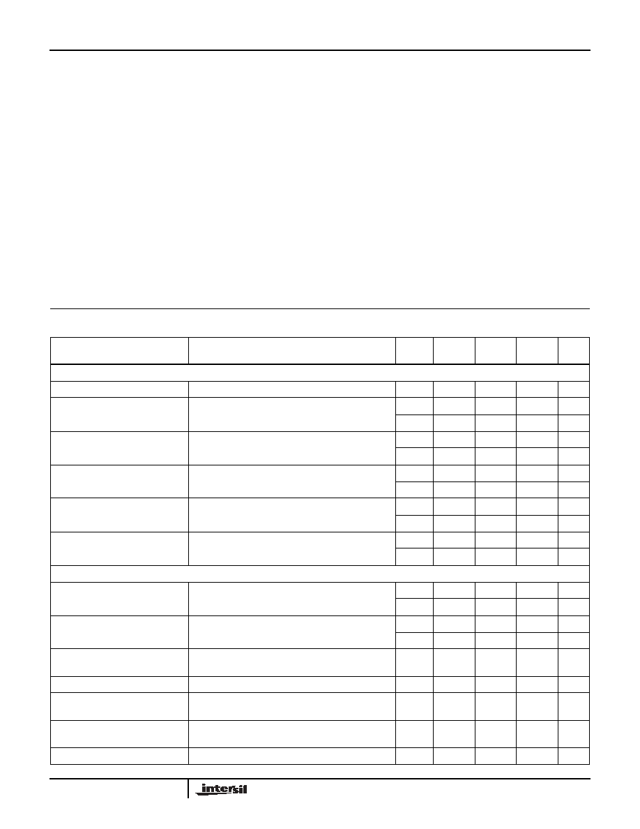
Electrical Specifications - 3V Supply
Test Conditions: V+ = +2.7V to +3.3V, GND = 0V, V
INH
= 1.4V, V
INL
= 0.5V (Notes 4, 6),
Unless Otherwise Specified
PARAMETER
TEST CONDITIONS
TEMP
(°C)
(NOTE 5)
MIN
TYP
(NOTE 5)
MAX
UNITS
ANALOG SWITCH CHARACTERISTICS
Analog Signal Range, V
ANALOG
Full
0
-
V+
V
ON Resistance, R
ON
V+ = 2.7V, I
COM
= 100mA, V
NO
or V
NC
= 0V to V+,
(See Figure 5)
25
-
0.3
0.45
Full
-
-
0.6
R
ON
Matching Between Channels,
R
ON
V+ = 2.7V, I
COM
= 100mA, V
NO
or V
NC
= Voltage at
max R
ON
, (Note 9)
25
-
0.04
0.08
Full
-
-
0.09
R
ON
Flatness, R
FLAT(ON)
V+ = 2.7V, I
COM
= 100mA, V
NO
or V
NC
= 0V to V+,
(Note 7)
25
-
0.06
0.15
Full
-
-
0.15
NO or NC OFF Leakage Current,
I
NO(OFF)
or I
NC(OFF)
V+ = 3.3V, V
COM
= 0.3V, 3V, V
NO
or V
NC
= 3V, 0.3V
25
-3
-
3
nA
Full
-20
-
20
nA
COM ON Leakage Current,
I
COM(ON)
V
+
= 3.3V, V
COM
= 0.3V, 3V, or V
NO
or V
NC
= 0.3V,
3V, or Floating
25
-4
-
4
nA
Full
-45
-
45
nA
DYNAMIC CHARACTERISTICS
Turn-ON Time, t
ON
V+ = 2.7V, V
NO
or V
NC
= 1.5V, R
L
= 50
, C
L
= 35pF,
(See Figure 1, Note 8)
25
-
11
17
ns
Full
-
-
20
ns
Turn-OFF Time, t
OFF
V+ = 2.7V, V
NO
or V
NC
= 1.5V, R
L
= 50
, C
L
= 35pF,
(See Figure 1, Note 8)
25
-
8
14
ns
Full
-
-
17
ns
Break-Before-Make Time Delay, t
D
V+ = 3.3V, V
NO
or V
NC
= 1.5V, R
L
= 50
, C
L
= 35pF,
(See Figure 3, Note 8)
Full
2
3
-
ns
Charge Injection, Q
C
L
= 1.0nF, V
G
= 0V, R
G
= 0
, (See Figure 2)
25
-
-82
-
pC
OFF Isolation
R
L
= 50
, C
L
= 5pF, f = 100kHz, V
COM
= 1V
RMS
,
(See Figure 4)
25
-
68
-
dB
Crosstalk (Channel-to-Channel)
R
L
= 50
, C
L
= 5pF, f = 100kHz, V
COM
= 1V
RMS
,
(See Figure 6)
25
-
-98
-
dB
Total Harmonic Distortion
f = 20Hz to 20kHz, V
COM
= 2V
P-P
, R
L
= 600
25
-
0.003
-
%
ISL83699
4
FN6094.3
November 5, 2004
NO or NC OFF Capacitance, C
OFF
f = 1MHz, V
NO
or V
NC
= V
COM
= 0V, (See Figure 7)
25
-
106
-
pF
COM ON Capacitance, C
COM(ON)
f = 1MHz, V
NO
or V
NC
= V
COM
= 0V, (See Figure 7)
25
-
212
-
pF
POWER SUPPLY CHARACTERISTICS
Power Supply Range
Full
1.65
3.6
V
Positive Supply Current, I+
V+ = 3.6V, V
IN
= 0V or V+
25
-
-
50
nA
Full
-
-
750
nA
DIGITAL INPUT CHARACTERISTICS
Input Voltage Low, V
INL
Full
-
-
0.5
V
Input Voltage High, V
INH
Full
1.4
-
-
V
Input Current, I
INH
, I
INL
V+ = 3.6V, V
IN
= 0V or V+ (Note 8)
Full
-0.5
-
0.5
µ
A
NOTES:
4. V
IN
= input voltage to perform proper function.
5. The algebraic convention, whereby the most negative value is a minimum and the most positive a maximum, is used in this data sheet.
6. Parts are 100% tested at +25°C. Limits across the full temperature range are guaranteed by design and correlation.
7. Flatness is defined as the difference between maximum and minimum value of on-resistance over the specified analog signal range.
8. Guaranteed but not tested.
9. R
ON
matching between channels is calculated by subtracting the channel with the highest max Ron value from the channel with lowest max Ron
value, between NC1 and NC2, NC3 and NC4 or between NO1 and NO2, NO3 and NO4.
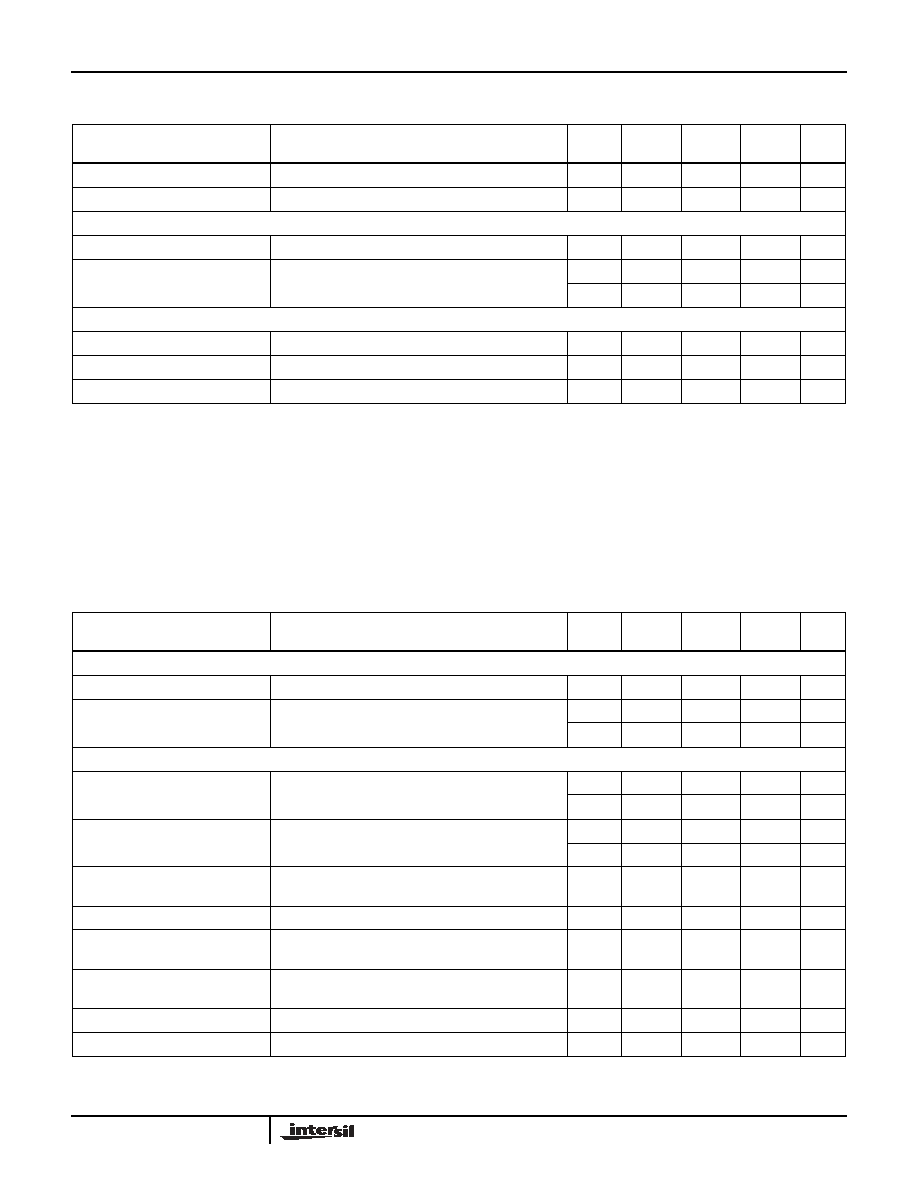
Electrical Specifications - 1.8V Supply
Test Conditions: V+ = +1.65V to +2V, GND = 0V, V
INH
= 1.0V, V
INL
= 0.4V (Notes 4, 6),
Unless Otherwise Specified
PARAMETER
TEST CONDITIONS
TEMP
(°C)
(NOTE 5)
MIN
TYP
(NOTE 5)
MAX
UNITS
ANALOG SWITCH CHARACTERISTICS
Analog Signal Range, V
ANALOG
Full
0
-
V+
V
ON Resistance, R
ON
V+ = 1.8V, I
COM
= 100mA, V
NO
or V
NC
= 0V to V+,
(See Figure 5)
25
-
0.45
0.8
Full
-
-
0.85
DYNAMIC CHARACTERISTICS
Turn-ON Time, t
ON
V+ = 1.65V, V
NO
or V
NC
= 1.0V, R
L
= 50
, C
L
= 35pF,
(See Figure 1, Note 8)
25
-
18
23
ns
Full
-
-
25
ns
Turn-OFF Time, t
OFF
V+ = 1.65V, V
NO
or V
NC
= 1.0V, R
L
= 50
, C
L
= 35pF,
(See Figure 1, Note 8)
25
-
10
15
ns
Full
-
-
18
ns
Break-Before-Make Time Delay, t
D
V+ = 2.0V, V
NO
or V
NC
= 1.0V, R
L
= 50
, C
L
= 35pF,
(See Figure 3, Note 8)
Full
2
5
-
ns
Charge Injection, Q
C
L
= 1.0nF, V
G
= 0V, R
G
= 0
, (See Figure 2)
25
-
-44
-
pC
OFF Isolation
R
L
= 50
, C
L
= 5pF, f = 100kHz, V
COM
= 1V
RMS
,
(See Figure 4)
25
-
68
-
dB
Crosstalk (Channel-to-Channel)
R
L
= 50
, C
L
= 5pF, f = 100kHz, V
COM
= 1V
RMS
,
(See Figure 6)
25
-
-98
-
dB
NO or NC OFF Capacitance, C
OFF
f = 1MHz, V
NO
or V
NC
= V
COM
= 0V, (See Figure 7)
25
-
106
-
pF
COM ON Capacitance, C
COM(ON)
f = 1MHz, V
NO
or V
NC
= V
COM
= 0V, (See Figure 7)
25
-
212
-
pF
Electrical Specifications - 3V Supply
Test Conditions: V+ = +2.7V to +3.3V, GND = 0V, V
INH
= 1.4V, V
INL
= 0.5V (Notes 4, 6),
Unless Otherwise Specified (Continued)
PARAMETER
TEST CONDITIONS
TEMP
(°C)
(NOTE 5)
MIN
TYP
(NOTE 5)
MAX
UNITS
ISL83699
5
FN6094.3
November 5, 2004
DIGITAL INPUT CHARACTERISTICS
Input Voltage Low, V
INL
Full
-
-
0.4
V
Input Voltage High, V
INH
Full
1.0
-
-
V
Input Current, I
INH
, I
INL
V+ = 2.0V, V
IN
= 0V or V+ (Note 8)
Full
-0.5
-
0.5
µ
A
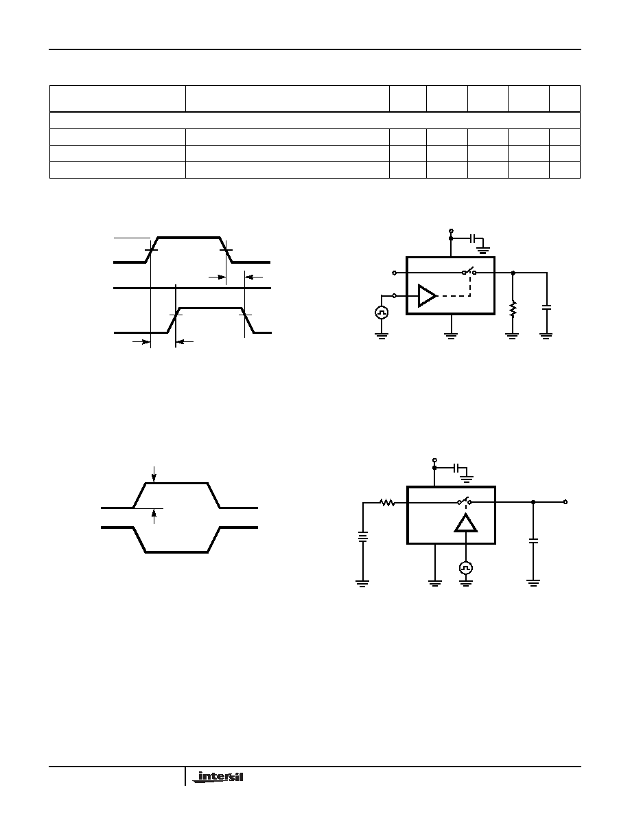
Test Circuits and Waveforms
Logic input waveform is inverted for switches that have the opposite
logic sense.
FIGURE 1A. MEASUREMENT POINTS
Repeat test for all switches. C
L
includes fixture and stray
capacitance.
FIGURE 1B. TEST CIRCUIT
FIGURE 1. SWITCHING TIMES
FIGURE 2A. MEASUREMENT POINTS
FIGURE 2B. TEST CIRCUIT
FIGURE 2. CHARGE INJECTION
Electrical Specifications - 1.8V Supply
Test Conditions: V+ = +1.65V to +2V, GND = 0V, V
INH
= 1.0V, V
INL
= 0.4V (Notes 4, 6),
Unless Otherwise Specified (Continued)
PARAMETER
TEST CONDITIONS
TEMP
(°C)
(NOTE 5)
MIN
TYP
(NOTE 5)
MAX
UNITS
50%
t
r
< 5ns
t
f
< 5ns
t
OFF
90%
V+
0V
V
NO
0V
t
ON
LOGIC
INPUT
SWITCH
INPUT
SWITCH
OUTPUT
90%
V
OUT
V
OUT
V(NO or NC)
R
L
R
L
R
ON
(
)
+
------------------------------
=
SWITCH
INPUT
LOGIC
INPUT
V
OUT
R
L
C
L
COM
NO or NC
IN
50
35pF
GND
V+
C
V
OUT
V
OUT
ON
OFF
ON
Q =
V
OUT
x C
L
SWITCH
OUTPUT
LOGIC
INPUT
V+
0V
C
L
V
OUT
R
G
V
G
GND
COM
NO or NC
V+
C
LOGIC
INPUT
IN
ISL83699