 | ÐлекÑÑоннÑй компоненÑ: FN9028 | СкаÑаÑÑ:  PDF PDF  ZIP ZIP |
Äîêóìåíòàöèÿ è îïèñàíèÿ www.docs.chipfind.ru
1
®
FN9028.1
ISL6160
InfiniBand +12V Bulk and +5V Auxiliary
Power Controller
The ISL6160 is designed to address the unique power
requirements of the InfiniBand (IB) industry initiative
providing independent power control of both the VB(bulk)
(+12V) and the VA(auxiliary) (+5V) power rails for a single
port. This device can be implemented in both IB Class I (non
isolated) and Class II (isolated) Power Topology applications.
The ISL6160, along with an N-Channel power MOSFET and
a minimal number of passive components provides soft
starting ramps of both the VB and VA voltages for an IB
module. It also provides accurate and consistent current
regulated outputs for a determined period of time before
latch-off in the presence of overcurrent (OC) conditions.
In addition the ISL6160 provides the enable signal to the on
module DC-DC converter either upon module insertion to
chassis or from a wake event request.
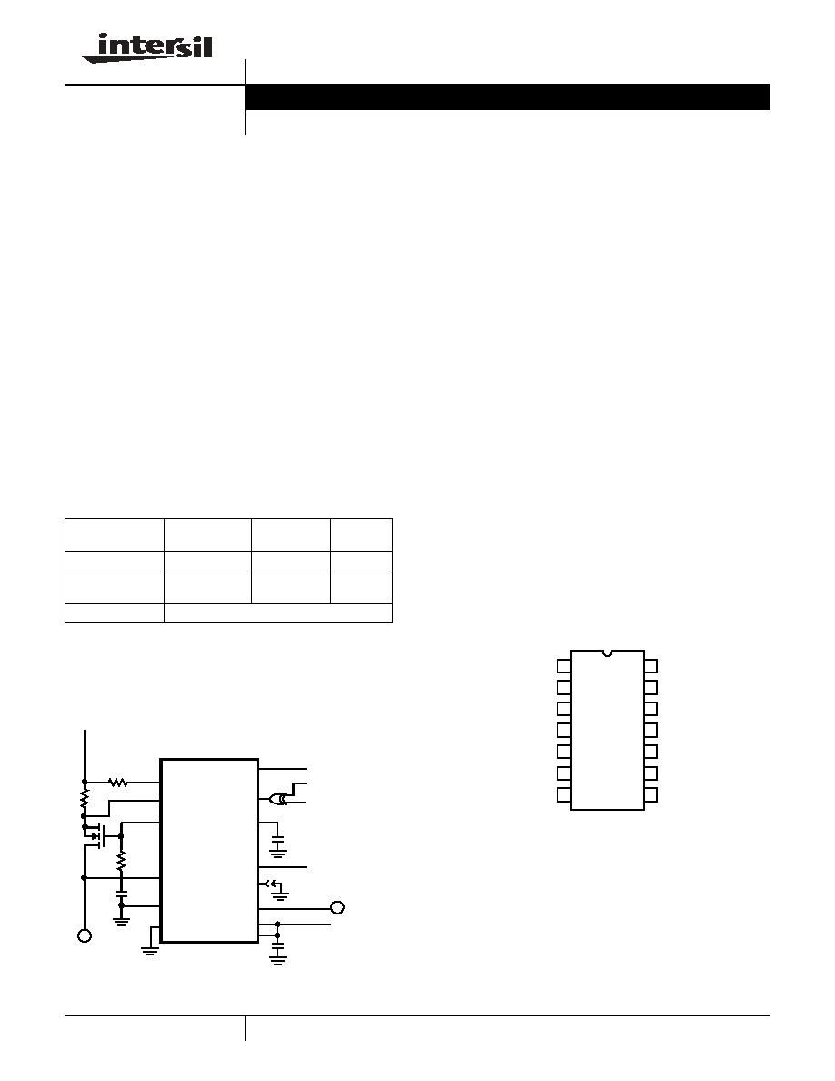
See Figure 1 for typical application usage.
Features
· VB Programmable Overcurrent Protection Regulation
Level for 25W and 50W Ports
· Internal Charge Pump Allows the Use of an N-Channel
MOSFET for VB Control
· VB Adjustable Turn-On Ramp
· Soft Start Overcurrent Protection During Turn-On
· Two Levels of VB Overcurrent Detection and Protection
· VA and VB Undervoltage Lock-Outs
· 0.125
Integrated Power N-Channel MOSFET VA Switch
· Accurate VA Current Sensing and Limiting (1A)
· Timed Current Regulation Period (VB Optional)
· VA Controlled Turn-On Ramp Time
· 1
µ
s Response Time to VB Secondary Rail Dead Short
·
Pb-free available
Applications
· InfiniBand VB and VA Voltage Control
· -48V and 5V Telecom
Pinout
ISL6160
(14 LEAD SOIC)
TOP VIEW
Ordering Information
PART NUMBER
TEMP. RANGE
(
o
C)
PACKAGE
PKG.
DWG. #
ISL6160CB
-40 to 85
14 Ld SOIC
M14.15
ISL6160CBZA
(See Note)
-40 to 85
14 Ld SOIC
(Pb-free)
M14.15
ISL6160EVAL2
IB Class I Power Topology Evaluation Platform
*Add "-T" suffix to part number for tape and reel packaging.
NOTE: Intersil Pb-free products employ special Pb-free material sets; molding
compounds/die attach materials and 100% matte tin plate termination finish, which
is compatible with both SnPb and Pb-free soldering operations. Intersil Pb-free
products are MSL classified at Pb-free peak reflow temperatures that meet or
exceed the Pb-free requirements of IPC/JEDEC J Std-020B.
FIGURE 1. TYPICAL APPLICATION USAGE
+
VB(ulk)
DC-DC EN
VA_FLTn
VA_ENn
VB_ON
VA_IN
VA_Out
ISET
ISEN
GATE
VB_IN
VB_Ret
+ VA(ux)
(OPT.)
VA_Ret
LOCAL PWR EN
VBxEN_L
VB SECONDARY RAIL TO DC-DC
TO DC-DC
CTIM
(OPT.)
GATE
VB_Ret
VB_IN
CTIM
DC-DC ENABLE
ISET
VA_FLTn
1
2
3
4
5
6
7
14
13
12
11
10
9
8
ISEN
VA_OUT
VA_ENn
VA_IN
NC
VA_Ret
VB_ON
Data Sheet
July 2004
CAUTION: These devices are sensitive to electrostatic discharge; follow proper IC Handling Procedures.
1-888-INTERSIL or 321-724-7143
|
Intersil (and design) is a registered trademark of Intersil Americas Inc.
Copyright © Intersil Americas Inc. 2001, 2004. All Rights Reserved
All other trademarks mentioned are the property of their respective owners.
2
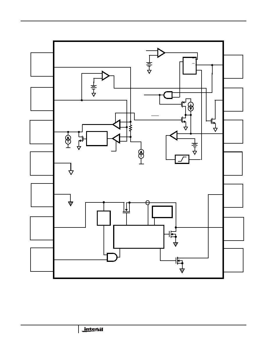
Simplified Block Diagram
VA_FLTn
VA_OUT
NC
+
-
ISET
ISEN
GATE
VB_RET
VB_IN
CTIM
DC-DC EN
VB_ON
CLIM
WOCLIM
ENABLE
OC
10
µA
FALLING
EDGE
DELAY
18V
+
-
V
REF
+
-
1.86V
12V
+
-
R
R
S
QN
Q
ENABLE
POR
VB
8V
RISING
EDGE
PULSE
+
-
+
-
UV
18V
20
µA
7.5K
+
-
+
-
20
µA
Q-PUMP
VA CURRENT AND TEMP.
POR
MONITORING, GATE AND
OUTPUT CONTROL
LOGIC
VA_RET
VA_IN
VA_ENn
ISL6160
3
Pin Descriptions
PIN NO.
DESIGNATOR
FUNCTION
DESCRIPTION
1
ISET
Current Set
Connect to the low side of the current sense resistor through the current limiting set resistor.
This pin functions as the current regulation level voltage programming pin.
CR Vth = R
ISET
X 20
µ
A
2
ISEN
Current Sense
Connect to the more positive end of sense resistor to measure the voltage drop across this
resistor.
3
GATE
External FET Gate
Drive Pin
Connect to the gate of the external N-Channel MOSFET. A capacitor from this node to
ground sets the turn-on ramp. At turn-on this capacitor will be charged to VB +5V by a 10
µ
A
current source.
4
VB_Ret
VB Chip Return
Bulk voltage ground
5
VA_Ret
VA Chip Return
Auxiliary voltage ground
6
VA_IN
VA Bias, Controlled
Supply Input,
Undervoltage Lock-Out
VA_IN provides the chip with +5V bias voltage. At VA < 2.5V, VA control functionality is
disabled, FAULT latch is cleared and floating and VA_OUT is held low.
7
VA_ENn
VA enable / disable
Connected to VA_Ret through the IB connector, VA is asserted on module when VA_ENn
is low. Cycle to reset after latch-off. POR also resets latch.
8
NC
NC
9
VA_OUT
Controlled Supply
Output
Upon an OC condition VA_OUT is current limited to 1A. Current limit response time is within
200
µ
s. VA_Out will remain in current limit for ~10mS before being latched off.
10
VA_ FLTn
Over Current Fault
Indicator
Over current fault indicator. VA_FLTn floats and is disabled until VA >2.5V. This output is
pulled low after the OC time-out period has expired and stays latched until module is
removed.
11
VB_IN
VB / Chip Supply
+12V Chip Supply.
12
CTIM
VB Current Regulation
Period
Connect a capacitor from this pin to ground. This capacitor determines the time delay
between an overcurrent event and chip output shutdown (current limit time-out). The
duration of current limit time-out (in seconds) = 93k
x C
TIM
(Farads).
13
DC-DC
ENABLE
VB_In Power Good
and DC-DC Enable
Signal
Indicates that the VB voltage on ISEN pin is within specification and enables the DC-DC
converter. DC-DC ENABLE is driven by an open drain N-Channel MOSFET and is pulled
low when VB Secondary rail (V
ISEN
) is not within specification.
14
VB_ON
VB Sequencer Enable
Control Signal
VB_ON is used to control and reset the VB supply to IB module. VB is asserted on, when
VB_ON pin is driven high or is open. After a latch-off VB is reset by a low level signal applied
to this pin. This input has 20
µ
A pull-up capability.
ISL6160
4
Absolute Maximum Ratings
Thermal Information
VB . . . . . . . . . . . . . . . . . . . . . . . . . . . . . . . . . . . . . . . . . . . . . +17.0V
GATE . . . . . . . . . . . . . . . . . . . . . . . . . . . . . . . . . . . . -0.3V to VB+8V
ISEN, PGOOD, VB_On, ISET . . . . . . . . . . . . . . . -0.3V to VB+ 0.3V
VA . . . . . . . . . . . . . . . . . . . . . . . . . . . . . . . . . . . . . . . . . . . . . . . 6.0V
VA_ENn, VA_FLTn . . . . . . . . . . . . . . . . . . . . . . . . . . . . . . -0.3V to 6V
VA_OUT. . . . . . . . . . . . . . . . . . . . . . . . . . . . . GND-0.3V to VA+0.3V
VA_Output Current . . . . . . . . . . . . . . . . . . . .Short Circuit Protected
ESD Classification . . . . . . . . . . . . . . . . . . . . . . . . . . . . . . 3kV (HBM)
Operating Conditions
VB Supply Voltage Range . . . . . . . . . . . . . . . . . . . . . . +10V to +14V
VA Supply Voltage Range . . . . . . . . . . . . . . . . . . . . . +4.5V to +5.5V
Temperature Range (T
A
) . . . . . . . . . . . . . . . . . . . . . . -40
o
C to 85
o
C
Thermal Resistance (Typical, Note 1)
JA
(
o
C/W)
SOIC Package . . . . . . . . . . . . . . . . . . . . . . . . . . . . .
90
Maximum Junction Temperature . . . . . . . . . . . . . . . . . . . . . . . 150
o
C
Maximum Storage Temperature Range . . . . . . . . . . -65
o
C to 150
o
C
Maximum Lead Temperature (Soldering 10s) . . . . . . . . . . . . . 300
o
C
(SOIC - Lead Tips Only)
CAUTION: Stresses above those listed in "Absolute Maximum Ratings" may cause permanent damage to the device. This is a stress only rating and operation of the
device at these or any other conditions above those indicated in the operational sections of this specification is not implied.
NOTES:
1. NOTE #1
JA
is measured with the component mounted on a low effective thermal conductivity test board in free air. See Tech
Brief TB379 for details.
2. All voltages are relative to GND, unless otherwise specified.
Electrical Specifications
Nominal VB = +12V, VA = +5V, T
A
= T
J
= -40
o
C - 85
o
C, Unless Otherwise Specified
PARAMETER
SYMBOL
TEST CONDITIONS
MIN
TYP
MAX
UNIT
S
+12V (VB) BULK SUPPLY CONTROL
ISET Current Source
I
ISET
18.5
20
21.5
µ
A
Current Limit Amp Offset Voltage
V
ISET
- V
ISEN
-4
0
4
mV
Severe Overcurrent Threshold
SOC_Vth
Above set current regulation voltage threshold
-
150
-
mV
Full Temp 25W VB Current Regulation
25W_ilim_ft
R
ISET
= 2.8k
1%, R
SENSE
= 20m
1%
2.2
2.8
3.4
A
Full Temp 50W VB Current Regulation
50W_ilim_ft
R
ISET
= 2.8k
1%, R
SENSE
= 10m
1%
4.5
5.6
6.7
A
Limited Temp 25W VB Current Regulation
25W_ilim_lt
R
ISET
= 2.8k
1%, R
SENSE
= 20m
1%,
T
J
= 15
o
C - 45
o
C
2.6
2.8
3.0
A
Limited Temp 50W VB Current Regulation
50W_ilim_lt
R
ISET
= 2.8k
1%, R
SENSE
= 10m
1%,
T
J
= 15
o
C - 45
o
C
5.2
5.6
6.0
A
GATE PARAMETERS
GATE Response Time to Severe
Overcurrent
Tr_gate_soc
V
RSENSE =
(150mV + CR Vth) to
V
GATE
to
10.8V
-
100
-
nS
GATE Response Time to Overcurrent
Tr_gate_oc
V
GATE
to 10.8V
-
600
-
ns
GATE Turn-On Current
I
GATE
V
GATE
to = 6V
8.4
10
11.6
µ
A
GATE Pull-Down Current
Igte_4v_oc
Overcurrent
45
75
-
mA
GATE Pull-Down Current
Igte_4V_soc
Severe Overcurrent
-
0.8
-
A
GATE High Voltage
Vgate_h
GATE Voltage
VB+4.5V VB+5V
-
V
VB PARAMETERS
IC Supply Current
I
VB
-
3
5
mA
VB POR Rising Threshold
VB
POR_L2H
VB Low to High
7.8
8.4
9
V
VB POR Falling Threshold
VB
POR_H2L
VB High to Low
7.5
8.1
8.7
V
VB POR Threshold Hysteresis
VB
POR_HYS
VB
POR_L2H -
VB
POR_H2L
0.1
0.3
0.6
V
DC-DC Enable Undervoltage Threshold
DCen
UV_VTH
9.2
9.6
10
V
VB_On Rising Threshold
PWR_Vth
1.4
1.7
2.0
V
VB_On Hysteresis
PWR_hys
-
170
-
mV
VB_On Pull-Up Voltage
PWRN_V
VB_On Pin Open
2.7
3.2
-
V
VB_On Pull-Up Current
PWRN_I
9
17
25
µ
A
ISL6160
5
ISL6160 Description and Operation
The ISL6160 is the first power supply sequencer for the
emerging InfiniBand module (IM) hot swap application. This IC
controls both the +12V VB(ulk) and +5V VA(ux) supplies
providing soft start during hot insertion and overcurrent (OC)
protection during operation.
For VB control and protection, the ISL6160 features include an
accurate current detecting comparator, current limiting for the
range of both 25W and 50W capable power ports, a current
regulated time delay to latch off and soft start turn-on ramp.
These features are all programmable with a minimum of
external passive components. The ISL6160 also includes
severe overcurrent protection that immediately shuts down the
MOSFET switch should there be a shorted IM load.
The VB_ON pin provides on-off control of the external VB
switch once VB_IN > 9V. Driving this pin high causes the gate
pin to charge the external gate capacitor with a 10uA current
setting the soft start ramp rate. Large capacitive loads can thus
be safely turned on with no inrush current spiking nor disruption
of the voltage supply rail.
The VB load current passes through an external current sense
resistor. When the voltage across the sense resistor exceeds
the user programmed ISET voltage threshold, the controller
enters current regulation (CR). The regulated current level is
fixed by the R
ISET
and R
SENSE
resistors. See Table 1 for
R
ISET
programming resistor value and the resulting nominal
CR threshold voltage.
During CR, the CTIM pin starts charging the time-out capacitor
with a 20
µ
A current source and the controller enters the delay
time to latch-off period. This feature allows transient currents
that exceed the designed limit to pass without immediately
CTIM PARAMETERS
C
TIM
Charging Current
C
TIM
_ichg0
V
CTIM
= 0V
16
20
23
µ
A
C
TIM
Fault Pull-Up Current
C
TIM
_ichg6
V
CTIM
= 6V
5
8
11
mA
Current Limit Time-Out Threshold Voltage
C
TIM
_Vth
CTIM Voltage
1.3
1.8
2.3
V
+5V AUXILIARY SUPPLY CONTROL
VA Integrated Switch On Resistance
r
DS(ON)
V
IN
= 5V, I
OUT
= 0.4A, T
A
= T
J
= 25
o
C
-
0.125
0.150
T
A
= T
J
= 85
o
C
-
0.160
0.200
Disabled Output Voltage
V
OUT_DIS
V
IN
= 5V, Switch Disabled, No Load
-
300
450
mV
V
OUT
Rising Rate
t_vout_rt
R
L
= 10
,
C
L
= 0.1
µ
F, 10%-90%
-
8
-
V/mS
Slow V
OUT
turn-off rate
Toff_svout
R
L
= 10
,
C
L
= 0.1
µ
F, 90%-10%
-
8
-
V/mS
Fast V
OUT
turn-off rate
Toff_fvout
R
L
= 10
,
C
L
= 0.1
µ
F, 90%-10%
-
4
-
V/uS
CURRENT CONTROL
Current Limit
Ilim
0.75
1
1.25
A
OC Regulation Settling Time
Tsett_ocr
R
L
= 5
,
C
L
= 0.1
µ
F to Within 10% of CR
-
1.5
-
ms
Severe OC Regulation Settling Time
Tsett_socr
R
L
< 1
,
C
L
= 0.1
µ
F to Within 10% of CR
-
100
-
µ
s
Over Current Latch-off Time
t
OC_loff
-
12
ms
I/O PARAMETERS
Fault Output Voltage
Vfault_hi
I
OUT
= 10mA
-
-
0.3
V
ENABLE High Threshold
Ven_vih
V
IN
= 5.5V
2.0
-
-
V
ENABLE Low Threshold
Ven_vil
V
IN
= 4.5V
-
-
0.8
V
ENABLE Input Current
Ien_i
ENABLE = 0V to 5V, V
IN
= 5V, T
J
> 25
o
C
-0.5
-
0.5
µ
A
BIAS PARAMETERS
Enabled VA_Iin Current
I
en_VA
Switches Closed, VA_Out = OPEN, T
J
>0
o
C
-
120
200
µ
A
Disabled VA_Iin Current
I
dis_VA
Switches Open, VA_Out = OPEN
-
1
5
µ
A
Undervoltage Lockout Threshold
V
UVLO
VIN Rising, Switch Enabled
1.7
2.25
2.5
V
UV Hysteresis
UV
HYS
50
100
-
mV
Electrical Specifications
Nominal VB = +12V, VA = +5V, T
A
= T
J
= -40
o
C - 85
o
C, Unless Otherwise Specified (Continued)
PARAMETER
SYMBOL
TEST CONDITIONS
MIN
TYP
MAX
UNIT
S
TABLE 1.
NOMINAL REGULATION LEVEL
(R
SENSE
= 0.020
)
R
ISET
RESISTOR
NOMINAL
OC Vth
CURRENT (A)
POWER (W)
1.0k
20mV
1
12
2.8k
56mV
2.8
33.6
3.48k
70mV
3.5
42
5.6k
112mV
5.6
67.2
NOTE: Nominal Vth = R
ISET
x 20
µ
A.
ISL6160