 | –≠–ª–µ–∫—Ç—Ä–æ–Ω–Ω—ã–π –∫–æ–º–ø–æ–Ω–µ–Ω—Ç: FRE260H | –°–∫–∞—á–∞—Ç—å:  PDF PDF  ZIP ZIP |
4-1
FRE260D, FRE260R,
FRE260H
31A, 200V, 0.080 Ohm, Rad Hard,
N-Channel Power MOSFETs
File Number
3259.1
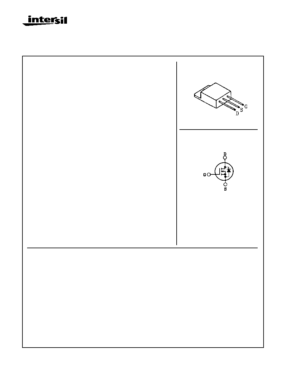
Package
TO-258AA
Symbol
Features
∑ 31A, 200V, RDS(on) = 0.080
∑ Second Generation Rad Hard MOSFET Results From New Design Concepts
∑ Gamma
- Meets Pre-Rad Specifications to 100KRAD(Si)
- Defined End Point Specs at 300KRAD(Si) and 1000KRAD(Si)
- Performance Permits Limited Use to 3000KRAD(Si)
∑ Gamma Dot
- Survives 3E9 RAD(Si)/sec at 80% BVDSS Typically
- Survives 2E12 Typically If Current Limited to IDM
∑ Photo Current
- 18.0nA Per-RAD(Si)/sec Typically
∑ Neutron
- Pre-RAD Specifications for 1E13 Neutrons/cm
2
- Usable to 1E14 Neutrons/cm
2
Description
The Intersil has designed a series of SECOND GENERATION hardened power
MOSFETs of both N and P channel enhancement types with ratings from 100V to
500V, 1A to 60A, and on resistance as low as 25m
. Total dose hardness is
offered at 100K RAD(Si) and 1000KRAD(Si) with neutron hardness ranging from
1E13 for 500V product to 1E14 for 100V product. Dose rate hardness (GAMMA
DOT) exists for rates to 1E9 without current limiting and 2E12 with current limiting.
This MOSFET is an enhancement-mode silicon-gate power field effect transistor of
the vertical DMOS (VDMOS) structure. It is specially designed and processed to
exhibit minimal characteristic changes to total dose (GAMMA) and neutron (n
o
)
exposures. Design and processing efforts are also directed to enhance survival to
heavy ion (SEU) and/or dose rate (GAMMA DOT) exposure.
This part may be supplied as a die or in various packages other than shown above.
Reliability screening is available as either non TX (commercial), TX equivalent of
MIL-S-19500, TXV equivalent of MIL-S-19500, or space equivalent of
MIL-S-19500. Contact the Intersil High-Reliability Marketing group for any desired
deviations from the data sheet.
Absolute Maximum Ratings
(TC = +25
o
C) Unless Otherwise Specified
FRE260D, R, H
UNITS
Drain-Source Voltage. . . . . . . . . . . . . . . . . . . . . . . . . . . . . . . . . . . . . . . . . . . . . . . . . . . . . . . VDS
200
V
Drain-Gate Voltage (RGS = 20k
). . . . . . . . . . . . . . . . . . . . . . . . . . . . . . . . . . . . . . . . . . . VDGR
200
V
Continuous Drain Current
TC = +25
o
C . . . . . . . . . . . . . . . . . . . . . . . . . . . . . . . . . . . . . . . . . . . . . . . . . . . . . . . . . . . . . .ID
TC = +100
o
C . . . . . . . . . . . . . . . . . . . . . . . . . . . . . . . . . . . . . . . . . . . . . . . . . . . . . . . . . . . . .ID
31
19
A
A
Pulsed Drain Current . . . . . . . . . . . . . . . . . . . . . . . . . . . . . . . . . . . . . . . . . . . . . . . . . . . . . . . IDM
93
A
Gate-Source Voltage . . . . . . . . . . . . . . . . . . . . . . . . . . . . . . . . . . . . . . . . . . . . . . . . . . . . . . .VGS
±
20
V
Maximum Power Dissipation
TC = +25
o
C . . . . . . . . . . . . . . . . . . . . . . . . . . . . . . . . . . . . . . . . . . . . . . . . . . . . . . . . . . . . . PT
TC = +100
o
C . . . . . . . . . . . . . . . . . . . . . . . . . . . . . . . . . . . . . . . . . . . . . . . . . . . . . . . . . . . . PT
Derated Above +25
o
C . . . . . . . . . . . . . . . . . . . . . . . . . . . . . . . . . . . . . . . . . . . . . . . . . . . . . . .
150
60
1.20
W
W
W/
o
C
Inductive Current, Clamped, L = 100
µ
H, (See Test Figure). . . . . . . . . . . . . . . . . . . . . . . . . . ILM
93
A
Continuous Source Current (Body Diode) . . . . . . . . . . . . . . . . . . . . . . . . . . . . . . . . . . . . . . . . . IS
31
A
Pulsed Source Current (Body Diode) . . . . . . . . . . . . . . . . . . . . . . . . . . . . . . . . . . . . . . . . . . ISM
93
A
Operating And Storage Temperature . . . . . . . . . . . . . . . . . . . . . . . . . . . . . . . . . . . . . TJC, TSTG
-55 to +150
o
C
Lead Temperature (During Soldering)
Distance > 0.063 in. (1.6mm) From Case, 10s Max. . . . . . . . . . . . . . . . . . . . . . . . . . . . . . . TL
300
o
C
June 1998
CAUTION: These devices are sensitive to electrostatic discharge; follow proper IC Handling Procedures.
http://www.intersil.com or 407-727-9207
|
Copyright
©
Intersil Corporation 1999

4-2
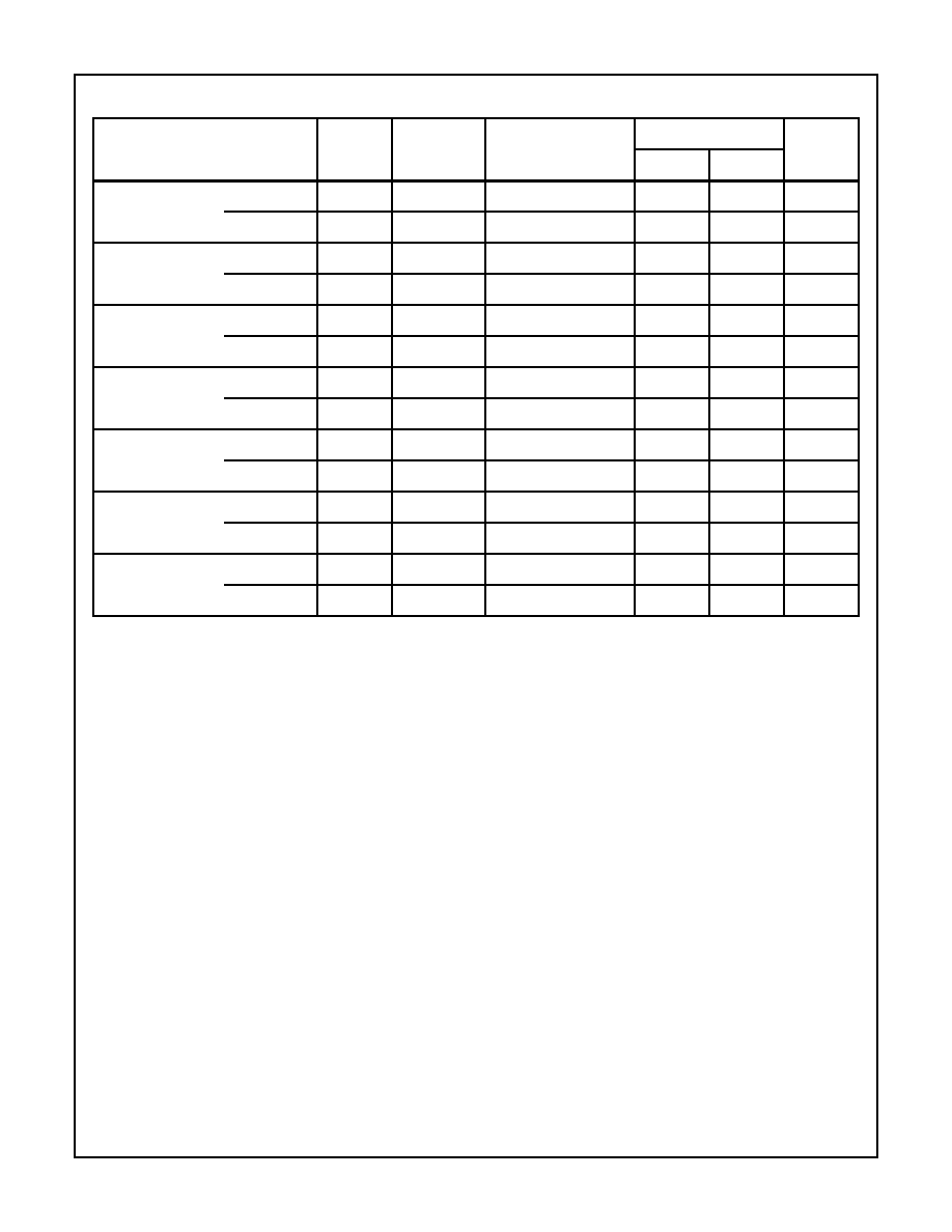
Pre-Radiation Electrical Specifications
TC = +25
o
C, Unless Otherwise Specified
PARAMETER
SYMBOL
TEST CONDITIONS
LIMITS
UNITS
MIN
MAX
Drain-Source Breakdown Volts
BVDSS
VGS = 0, ID = 1mA
200
-
V
Gate-Treshold Volts
VGS(th)
VDS = VGS, ID = 1mA
2.0
4.0
V
Gate-Body Leakage Forward
IGSSF
VGS = +20V
-
100
nA
Gate-Body Leakage Reverse
IGSSR
VGS = -20V
-
100
nA
Zero-Gate Voltage Drain Current
IDSS1
IDSS2
IDSS3
VDS = 200V, VGS = 0
VDS = 160V, VGS = 0
VDS = 160V, VGS = 0,Tc = +125
o
C
-
-
-
1
0.025
0.25
mA
Rated Avalanche Current
IAR
Time = 20
µ
s
-
93
A
Drain-Source On-State Volts
VDS(on)
VGS = 10V, ID = 31A
-
2.60
V
Drain-Source On Resistance
RDS(on)
VGS = 10V, ID = 19A
-
0.080
Turn-On Delay Time
td(on)
VDD = 100V, ID = 31A
Pulse Width = 3
µ
s
Period = 300
µ
s Rg = 10
0 < VGS < 10 (See Test Circuit)
-
100
ns
Rise Time
tr
-
250
Turn-Off Delay Time
td(off)
-
600
Fall Time
tf
-
300
Gate-Charge Threshold
QG(th)
VDD = 100V, ID = 31A
IGS1 = IGS2
0 < Vgs < 20
6
24
ns
Gate-Charge On State
QG(on)
110
440
Gate-Charge Total
QGM
214
856
Plateau Voltage
VGP
3
12
V
Gate-Charge Source
QGS
20
80
nc
Gate-Charge Drain
QGD
46
184
Diode Forward Voltage
VSD
ID = 31A, VGD = 0
0.6
1.8
V
Reverse Recovery Time
TT
I = 31A; di/dt = 100A/
µ
s
-
1200
ns
Junction-To-Case
R
jc
-
-
0.83
o
C/W
Junction-To-Ambient
R
ja
Free Air Operation
-
48
FIGURE 1. RESISTIVE SWITCHING TEST CIRCUIT
FIGURE 2. UNCLAMPED ENERGY TEST CIRCUIT
V
DS
DUT
R
GS
0V
V
GS
= 12V
V
DD
R
L
t
P
V
GS
20V
L
+
-
V
DS
V
DD
DUT
VARY t
P
TO OBTAIN
REQUIRED PEAK I
AS
0V
50
50
50V-150V
I
AS
+
-
ELECTRONIC SWITCH OPENS
WHEN I
AS
IS REACHED
CURRENT
TRANSFORMER
FRE260D, FRE260R, FRE260H
4-3
Post-Radiation Electrical Specifications
TC = +25
o
C, Unless Otherwise Specified
PARAMETER
SYMBOL
TYPE
TEST CONDITIONS
LIMITS
UNITS
MIN
MAX
Drain-Source
Breakdown Volts
(Note 4, 6)
BVDSS
FRE260D, R
VGS = 0, ID = 1mA
200
-
V
(Note 5, 6)
BVDSS
FRE260H
VGS = 0, ID = 1mA
190
-
V
Gate-Source
Threshold Volts
(Note 4, 6)
VGS(th)
FRE260D, R
VGS = VDS, ID = 1mA
2.0
4.0
V
(Note 3, 5, 6)
VGS(th)
FRE260H
VGS = VDS, ID = 1mA
1.5
4.5
V
Gate-Body
Leakage Forward
(Note 4, 6)
IGSSF
FRE260D, R
VGS = 20V, VDS = 0
-
100
nA
(Note 5, 6)
IGSSF
FRE260H
VGS = 20V, VDS = 0
-
200
nA
Gate-Body
Leakage Reverse
(Note 2, 4, 6)
IGSSR
FRE260D, R
VGS = -20V, VDS = 0
-
100
nA
(Note 2, 5, 6)
IGSSR
FRE260H
VGS = -20V, VDS = 0
-
200
nA
Zero-Gate Voltage
Drain Current
(Note 4, 6)
IDSS
FRE260D, R
VGS = 0, VDS = 160V
-
25
µ
A
(Note 5, 6)
IDSS
FRE260H
VGS = 0, VDS = 160V
-
100
µ
A
Drain-Source
On-State Volts
(Note 1, 4, 6)
VDS(on)
FRE260D, R
VGS = 10V, ID = 31A
-
2.60
V
(Note 1, 5, 6)
VDS(on)
FRE260H
VGS = 16V, ID = 31A
-
3.90
V
Drain-Source
On Resistance
(Note 1, 4, 6)
RDS(on)
FRE260D, R
VGS = 10V, ID = 19A
-
0.080
(Note 1, 5, 6)
RDS(on)
FRE260H
VGS = 14V, ID = 19A
-
0.120
NOTES:
1. Pulse test, 300
µ
s max
2. Absolute value
3. Gamma = 300KRAD(Si)
4. Gamma = 10KRAD(Si) for "D", 100KRAD(Si) for "R". Neutron = 1E13
5. Gamma = 1000KRAD(Si). Neutron = 1E13
6. Insitu Gamma bias must be sampled for both VGS = +10V, VDS = 0V and VGS = 0V, VDS = 80% BVDSS
7. Gamma data taken 1/02/90 on TA 17662 devices by GE ASTRO SPACE; EMC/SURVIVABILITY LABORATORY; KING OF PRUSSIA,
PA 19401
8. Single event drain burnout testing by Titus, J.L., et al of NWSC, Crane, IN at Brookhaven Nat. Lab. Dec 11-14, 1989
9. Neutron derivation, INTERSIL Application Note AN-8831, Oct. 1988
FRE260D, FRE260R, FRE260H

4-4
Performance Curves
FRE260D, FRE260R, FRE260H

4-5
FRE260D, FRE260R, FRE260H
Rad Hard Data Packages - Intersil Power Transistors
TXV Equivalent
1. Rad Hard TXV Equivalent - Standard Data Package
A. Certificate of Compliance
B. Assembly Flow Chart
C. Preconditioning - Attributes Data Sheet
D. Group A
- Attributes Data Sheet
E. Group B
- Attributes Data Sheet
F. Group C
- Attributes Data Sheet
G. Group D
- Attributes Data Sheet
2. Rad Hard TXV Equivalent - Optional Data Package
A. Certificate of Compliance
B. Assembly Flow Chart
C. Preconditioning - Attributes Data Sheet
- Precondition Lot Traveler
- Pre and Post Burn-In Read and Record
Data
D. Group A
- Attributes Data Sheet
- Group A Lot Traveler
E. Group B
- Attributes Data Sheet
- Group B Lot Traveler
- Pre and Post Read and Record Data for
Intermittent Operating Life (Subgroup B3)
- Bond Strength Data (Subgroup B3)
- Pre and Post High Temperature Operating
Life Read and Record Data (Subgroup B6)
F. Group C
- Attributes Data Sheet
- Group C Lot Traveler
- Pre and Post Read and Record Data for
Intermittent Operating Life (Subgroup C6)
- Bond Strength Data (Subgroup C6)
G. Group D
- Attributes Data Sheet
- Group D Lot Traveler
- Pre and Post RAD Read and Record Data
Class S - Equivalents
1. Rad Hard "S" Equivalent - Standard Data Package
A. Certificate of Compliance
B. Serialization Records
C. Assembly Flow Chart
D. SEM Photos and Report
E.
Preconditioning Attributes Data Sheet
Hi-Rel Lot Traveler
HTRB - Hi Temp Gate Stress Post Reverse
Bias Data and Delta Data
HTRB - Hi Temp Drain Stress Post Reverse
Bias Delta Data
F. Group A
- Attributes Data Sheet
G. Group B
- Attributes Data Sheet
H. Group C
- Attributes Data Sheet
I. Group D
- Attributes Data Sheet
2. Rad Hard Max. "S" Equivalent - Optional Data Package
A. Certificate of Compliance
B. Serialization Records
C. Assembly Flow Chart
D. SEM Photos and Report
E. Preconditioning - Attributes Data Sheet
- Hi-Rel Lot Traveler
- HTRB - Hi Temp Gate Stress Post
Reverse Bias Data and Delta Data
- HTRB - Hi Temp Drain Stress Post
Reverse Bias Delta Data
- X-Ray and X-Ray Report
F. Group A
- Attributes Data Sheet
- Hi-Rel Lot Traveler
- Subgroups A2, A3, A4, A5 and A7 Data
G. Group B
- Attributes Data Sheet
- Hi-Rel Lot Traveler
- Subgroups B1, B3, B4, B5 and B6 Data
H. Group C
- Attributes Data Sheet
- Hi-Rel Lot Traveler
- Subgroups C1, C2, C3 and C6 Data
I. Group D
- Attributes Data Sheet
- Hi-Rel Lot Traveler
- Pre and Post Radiation Data