 | –≠–ª–µ–∫—Ç—Ä–æ–Ω–Ω—ã–π –∫–æ–º–ø–æ–Ω–µ–Ω—Ç: FRF450H | –°–∫–∞—á–∞—Ç—å:  PDF PDF  ZIP ZIP |

4-1
FRF450D, FRF450R,
FRF450H
9A, 500V, 0.615 Ohm, Rad Hard,
N-Channel Power MOSFETs
File Number
3237.1
Package
TO-254AA
Symbol
CAUTION: Beryllia Warning per MIL-S-19500
refer to package specifications.
Features
∑ 9A, 500V, RDS(on) = 0.615
∑ Second Generation Rad Hard MOSFET Results From New Design Concepts
∑ Gamma
- Meets Pre-Rad Specifications to 100KRAD(Si)
- Defined End Point Specs at 300KRAD(Si) and 1000KRAD(Si)
- Performance Permits Limited Use to 3000KRAD(Si)
∑ Gamma Dot
- Survives 3E9RAD(Si)/sec at 80% BVDSS Typically
- Survives 2E12 Typically If Current Limited to IDM
∑ Photo Current
- 30.0nA Per-RAD(Si)/sec Typically
∑ Neutron
- Pre-RAD Specifications for 3E12 Neutrons/cm
2
- Usable to 3E13 Neutrons/cm
2
Description
The Intersil has designed a series of SECOND GENERATION hardened power
MOSFETs of both N and P channel enhancement types with ratings from 100V to
500V, 1A to 60A, and on resistance as low as 25m
. Total dose hardness is
offered at 100K RAD(Si) and 1000KRAD(Si) with neutron hardness ranging from
1E13n/cm
2
for 500V product to 1E14n/cm
2
for 100V product. Dose rate hardness
(GAMMA DOT) exists for rates to 1E9 without current limiting and 2E12 with cur-
rent limiting.
This MOSFET is an enhancement-mode silicon-gate power field effect transistor of
the vertical DMOS (VDMOS) structure. It is specially designed and processed to
exhibit minimal characteristic changes to total dose (GAMMA) and neutron (n
o
)
exposures. Design and processing efforts are also directed to enhance survival to
heavy ion (SEE) and/or dose rate (GAMMA DOT) exposure.
This part may be supplied as a die or in various packages other than shown above.
Reliability screening is available as either non TX (commercial), TX equivalent of
MIL-S-19500, TXV equivalent of MIL-S-19500, or space equivalent of
MIL-S-19500. Contact the Intersil High-Reliability Marketing group for any desired
deviations from the data sheet.
Absolute Maximum Ratings
(TC = +25
o
C) Unless Otherwise Specified
FRF450D, R, H
UNITS
Drain-Source Voltage. . . . . . . . . . . . . . . . . . . . . . . . . . . . . . . . . . . . . . . . . . . . . . . . . . . . . . . VDS
500
V
Drain-Gate Voltage (RGS = 20k
). . . . . . . . . . . . . . . . . . . . . . . . . . . . . . . . . . . . . . . . . . . VDGR
500
V
Continuous Drain Current
TC = +25
o
C . . . . . . . . . . . . . . . . . . . . . . . . . . . . . . . . . . . . . . . . . . . . . . . . . . . . . . . . . . . . . .ID
TC = +100
o
C . . . . . . . . . . . . . . . . . . . . . . . . . . . . . . . . . . . . . . . . . . . . . . . . . . . . . . . . . . . . .ID
9
6
A
A
Pulsed Drain Current . . . . . . . . . . . . . . . . . . . . . . . . . . . . . . . . . . . . . . . . . . . . . . . . . . . . . . . IDM
27
A
Gate-Source Voltage . . . . . . . . . . . . . . . . . . . . . . . . . . . . . . . . . . . . . . . . . . . . . . . . . . . . . . .VGS
±
20
V
Maximum Power Dissipation
TC = +25
o
C . . . . . . . . . . . . . . . . . . . . . . . . . . . . . . . . . . . . . . . . . . . . . . . . . . . . . . . . . . . . . PT
TC = +100
o
C . . . . . . . . . . . . . . . . . . . . . . . . . . . . . . . . . . . . . . . . . . . . . . . . . . . . . . . . . . . . PT
Derated Above +25
o
C . . . . . . . . . . . . . . . . . . . . . . . . . . . . . . . . . . . . . . . . . . . . . . . . . . . . . . .
125
50
1.00
W
W
W/
o
C
Inductive Current, Clamped, L = 100
µ
H, (See Test Figure). . . . . . . . . . . . . . . . . . . . . . . . . . ILM
27
A
Continuous Source Current (Body Diode) . . . . . . . . . . . . . . . . . . . . . . . . . . . . . . . . . . . . . . . . . IS
9
A
Pulsed Source Current (Body Diode) . . . . . . . . . . . . . . . . . . . . . . . . . . . . . . . . . . . . . . . . . . ISM
27
A
Operating And Storage Temperature . . . . . . . . . . . . . . . . . . . . . . . . . . . . . . . . . . . . . TJC, TSTG
-55 to +150
o
C
Lead Temperature (During Soldering)
Distance > 0.063 in. (1.6mm) From Case, 10s Max. . . . . . . . . . . . . . . . . . . . . . . . . . . . . . . TL
300
o
C
June 1998
CAUTION: These devices are sensitive to electrostatic discharge; follow proper IC Handling Procedures.
http://www.intersil.com or 407-727-9207
|
Copyright
©
Intersil Corporation 1999

4-2
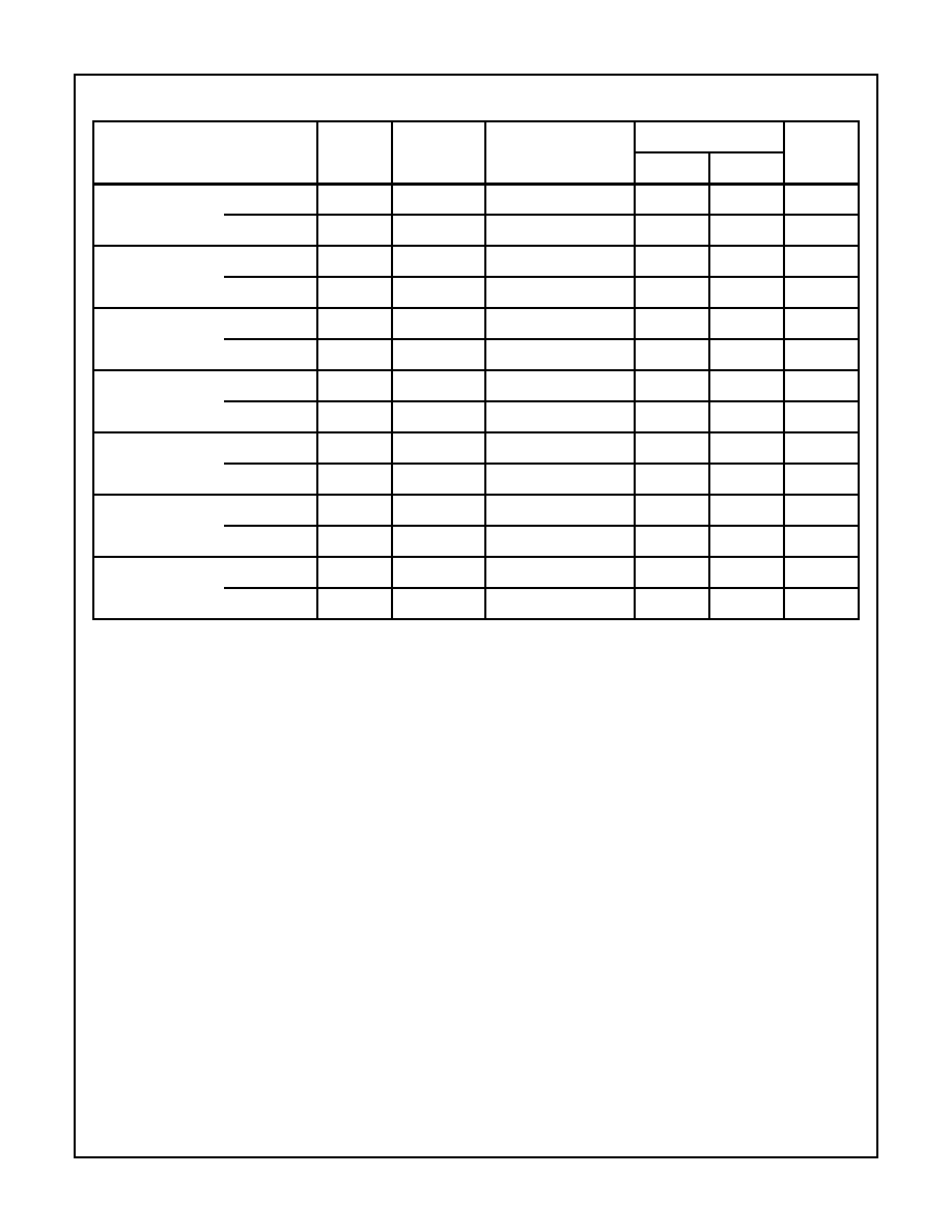
Pre-Radiation Electrical Specifications
TC = +25
o
C, Unless Otherwise Specified
PARAMETER
SYMBOL
TEST CONDITIONS
LIMITS
UNITS
MIN
MAX
Drain-Source Breakdown Volts
BVDSS
VGS = 0, ID = 1mA
500
-
V
Gate-Threshold Volts
VGS(th)
VDS = VGS, ID = 1mA
2.0
4.0
V
Gate-Body Leakage Forward
IGSSF
VGS = +20V
-
100
nA
Gate-Body Leakage Reverse
IGSSR
VGS = -20V
-
100
nA
Zero-Gate Voltage
Drain Current
IDSS1
IDSS2
IDSS3
VDS = 500V, VGS = 0
VDS = 400V, VGS = 0
VDS = 400V, VGS = 0, TC = +125
o
C
-
-
-
1
0.025
0.25
mA
Rated Avalanche Current
IAR
Time = 20
µ
s
-
27
A
Drain-Source On-State Volts
VDS(on)
VGS = 10V, ID = 9A
-
5.81
V
Drain-Source On Resistance
RDS(on)
VGS = 10V, ID = 6A
-
0.615
Turn-On Delay Time
td(on)
VDD = 250V, ID = 9A
-
148
ns
Rise Time
tr
Pulse Width = 3
µ
s
-
196
Turn-Off Delay Time
td(off)
Period = 300
µ
s, Rg = 25
-
800
Fall Time
tf
0
VGS
10 (See Test Circuit)
-
180
Gate-Charge Threshold
QG(th)
VDD = 250V, ID = 9A
IGS1 = IGS2
0
VGS
20
4
16
nc
Gate-Charge On State
QG(on)
66
264
Gate-Charge Total
QGM
121
486
Plateau Voltage
VGP
3
12
V
Gate-Charge Source
QGS
14
56
nc
Gate-Charge Drain
QGD
31
126
Diode Forward Voltage
VSD
ID = 9A, VGD = 0
0.6
1.8
V
Reverse Recovery Time
TT
I = 9A; di/dt = 100A/
µ
s
-
3000
ns
Junction-To-Case
R
jc
-
1.0
o
C/W
Junction-To-Ambient
R
ja
Free Air Operation
-
48
FIGURE 1. RESISTIVE SWITCHING TEST CIRCUIT
FIGURE 2. UNCLAMPED ENERGY TEST CIRCUIT
V
DS
DUT
R
GS
0V
V
GS
= 12V
V
DD
R
L
t
P
V
GS
20V
L
+
-
V
DS
V
DD
DUT
VARY t
P
TO OBTAIN
REQUIRED PEAK I
AS
0V
50
50
50V-150V
I
AS
+
-
ELECTRONIC SWITCH OPENS
WHEN I
AS
IS REACHED
CURRENT
TRANSFORMER
FRF450D, FRF450R, FRF450H
4-3
Post-Radiation Electrical Specifications
TC = +25
o
C, Unless Otherwise Specified
PARAMETER
SYMBOL
TYPE
TEST CONDITIONS
LIMITS
UNITS
MIN
MAX
Drain-Source
Breakdown Volts
(Note 4, 6)
BVDSS
FRF450D, R
VGS = 0, ID = 1mA
500
-
V
(Note 5, 6)
BVDSS
FRF450H
VGS = 0, ID = 1mA
475
-
V
Gate-Source
Threshold Volts
(Note 4, 6)
VGS(th)
FRF450D, R
VGS = VDS, ID = 1mA
2.0
4.0
V
(Note 3, 5, 6)
VGS(th)
FRF450H
VGS = VDS, ID = 1mA
1.5
4.5
V
Gate-Body
Leakage Forward
(Note 4, 6)
IGSSF
FRF450D, R
VGS = 20V, VDS = 0
-
100
nA
(Note 5, 6)
IGSSF
FRF450H
VGS = 20V, VDS = 0
-
200
nA
Gate-Body
Leakage Reverse
(Note 2, 4, 6)
IGSSR
FRF450D, R
VGS = -20V, VDS = 0
-
100
nA
(Note 2, 5, 6)
IGSSR
FRF450H
VGS = -20V, VDS = 0
-
200
nA
Zero-Gate Voltage
Drain Current
(Note 4, 6)
IDSS
FRF450D, R
VGS = 0, VDS = 400V
-
25
µ
A
(Note 5, 6)
IDSS
FRF450H
VGS = 0, VDS = 400V
-
100
µ
A
Drain-Source
On-State Volts
(Note 1, 4, 6)
VDS(on)
FRF450D, R
VGS = 10V, ID = 9A
-
5.81
V
(Note 1, 5, 6)
VDS(on)
FRF450H
VGS = 16V, ID = 9A
-
8.30
V
Drain-Source
On Resistance
(Note 1, 4, 6)
RDS(on)
FRF450D, R
VGS = 10V, ID = 6A
-
0.615
(Note 1, 5, 6)
RDS(on)
FRF450H
VGS = 14V, ID = 6A
-
0.879
NOTES:
1. Pulse test, 300
µ
s max
2. Absolute value
3. Gamma = 300KRAD(Si)
4. Gamma = 10KRAD(Si) for "D", 100KRAD(Si) for "R". Neutron = 3E12
5. Gamma = 1000KRAD(Si). Neutron = 3E12
6. Insitu Gamma bias must be sampled for both VGS = +10V, VDS = 0V and VGS = 0V, VDS = 80% BVDSS
7. Gamma data taken 12/18/89 on TA 17655 devices by GE ASTRO SPACE; EMC/SURVIVABILITY LABORATORY; KING OF PRUSSIA,
PA 19401
8. Single event drain burnout testing by Titus, J.L., et al of NWSC, Crane, IN at Brookhaven Nat. Lab. Dec 11-14, 1989
9. Neutron derivation, INTERSIL Application note AN-8831, Oct. 1988
FRF450D, FRF450R, FRF450H
4-4
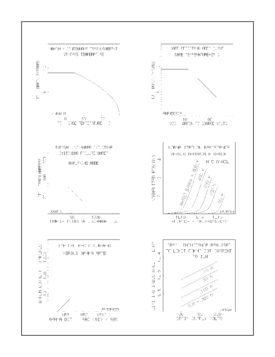
Typical Performance Characteristics
FRF450D, FRF450R, FRF450H

4-5
FRF450D, FRF450R, FRF450H
Rad Hard Data Packages - Intersil Power Transistors
TXV Equivalent
1. Rad Hard TXV Equivalent - Standard Data Package
A. Certificate of Compliance
B. Assembly Flow Chart
C. Preconditioning - Attributes Data Sheet
D. Group A
- Attributes Data Sheet
E. Group B
- Attributes Data Sheet
F. Group C
- Attributes Data Sheet
G. Group D
- Attributes Data Sheet
2. Rad Hard TXV Equivalent - Optional Data Package
A. Certificate of Compliance
B. Assembly Flow Chart
C. Preconditioning - Attributes Data Sheet
- Precondition Lot Traveler
- Pre and Post Burn-In Read and Record
Data
D. Group A
- Attributes Data Sheet
- Group A Lot Traveler
E. Group B
- Attributes Data Sheet
- Group B Lot Traveler
- Pre and Post Read and Record Data for
Intermittent Operating Life (Subgroup B3)
- Bond Strength Data (Subgroup B3)
- Pre and Post High Temperature Operating
Life Read and Record Data (Subgroup B6)
F. Group C
- Attributes Data Sheet
- Group C Lot Traveler
- Pre and Post Read and Record Data for
Intermittent Operating Life (Subgroup C6)
- Bond Strength Data (Subgroup C6)
G. Group D
- Attributes Data Sheet
- Group D Lot Traveler
- Pre and Post RAD Read and Record Data
Class S - Equivalents
1. Rad Hard "S" Equivalent - Standard Data Package
A. Certificate of Compliance
B. Serialization Records
C. Assembly Flow Chart
D. SEM Photos and Report
E.
Preconditioning Attributes Data Sheet
Hi-Rel Lot Traveler
HTRB - Hi Temp Gate Stress Post Reverse
Bias Data and Delta Data
HTRB - Hi Temp Drain Stress Post Reverse
Bias Delta Data
F. Group A
- Attributes Data Sheet
G. Group B
- Attributes Data Sheet
H. Group C
- Attributes Data Sheet
I. Group D
- Attributes Data Sheet
2. Rad Hard Max. "S" Equivalent - Optional Data Package
A. Certificate of Compliance
B. Serialization Records
C. Assembly Flow Chart
D. SEM Photos and Report
E. Preconditioning - Attributes Data Sheet
- Hi-Rel Lot Traveler
- HTRB - Hi Temp Gate Stress Post
Reverse Bias Data and Delta Data
- HTRB - Hi Temp Drain Stress Post
Reverse Bias Delta Data
- X-Ray and X-Ray Report
F. Group A
- Attributes Data Sheet
- Hi-Rel Lot Traveler
- Subgroups A2, A3, A4, A5 and A7 Data
G. Group B
- Attributes Data Sheet
- Hi-Rel Lot Traveler
- Subgroups B1, B3, B4, B5 and B6 Data
H. Group C
- Attributes Data Sheet
- Hi-Rel Lot Traveler
- Subgroups C1, C2, C3 and C6 Data
I. Group D
- Attributes Data Sheet
- Hi-Rel Lot Traveler
- Pre and Post Radiation Data