 | ÐлекÑÑоннÑй компоненÑ: FRX130D1 | СкаÑаÑÑ:  PDF PDF  ZIP ZIP |
Äîêóìåíòàöèÿ è îïèñàíèÿ www.docs.chipfind.ru
1
FRX130D, FRX130R,
FRX130H
Radiation Hardened
N-Channel Power MOSFETs
April 1998
Features
· 6A, 100V, r
DS(ON)
=
0.180
· Second Generation Rad Hard MOSFET Results From
New Design Concepts
· Gamma
- Meets Pre-RAD Specifications to 100K RAD (Si)
- Defined End-Point Specs at 300K RAD (Si) and
1000K RAD (Si)
- Performance Permits Limited Use to 3000K RAD (Si)
· Dose Rate
- Typically Survives 3E9 RAD (Si)/s at 80% BV
DSS
- Typically Survives 2E12 if Current Limited to I
DM
· Photo Current
- 1.50nA Per-RAD (Si)/s Typically
· Neutron
- Maintain Pre-RAD Specifications
for 3E13 Neutrons/cm
2
- Usable to 3E14 Neutrons/cm
2
Description
The Intersil has designed a series of SECOND GENERA-
TION hardened power MOSFETs of both N-Channel and
P-Channel enhancement types with ratings from 100V to
500V, 1A to 60A, and on resistance as low as 25m
. Total
dose hardness is offered at 100K RAD (Si) and 1000K RAD
(Si) with neutron hardness ranging from 1E13n/cm
2
for
500V product to 1E14n/cm
2
for 100V product. Dose rate
hardness (GAMMA DOT) exists for rates to 1E9 without
current limiting and 2E12 with current limiting.
This MOSFET is an enhancement-mode silicon-gate power
field effect transistor of the vertical DMOS (VDMOS) struc-
ture. It is specially designed and processed to exhibit mini-
mal characteristic changes to total dose (GAMMA) and
neutron (n
o
) exposures. Design and processing efforts are
also directed to enhance survival to heavy ion (SEU) and/or
dose rate (GAMMA DOT) exposure.
This part may be supplied as a die or in various packages
other than shown above. Reliability screening is available
as either non TX (commercial), TX equivalent of MIL-S-
19500, TXV equivalent of MIL-S-19500, or space equiva-
lent of MIL-S-19500. Contact the Intersil High-Reliability
Marketing group for any desired deviations from the data
sheet.
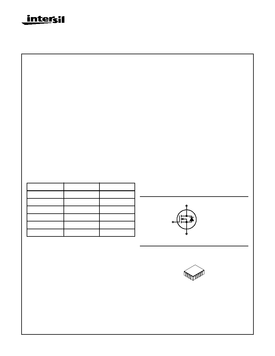
Symbol
Package
18 LEAD CLCC
Ordering Information
PART NUMBER
PACKAGE
BRAND
FRX130D1
18 Ld CLCC
FRX130D1
FRX130D3
18 Ld CLCC
FRX130D3
FRX130R1
18 Ld CLCC
FRX130R1
FRX130R3
18 Ld CLCC
FRX130R3
FRX130R4
18 Ld CLCC
FRX130R4
FRX130H4
18 Ld CLCC
FRX130H4
D
G
S
File Number
3144.3
CAUTION: These devices are sensitive to electrostatic discharge; follow proper IC Handling Procedures.
http://www.intersil.com or 407-727-9207
|
Copyright
©
Intersil Corporation 1999
2
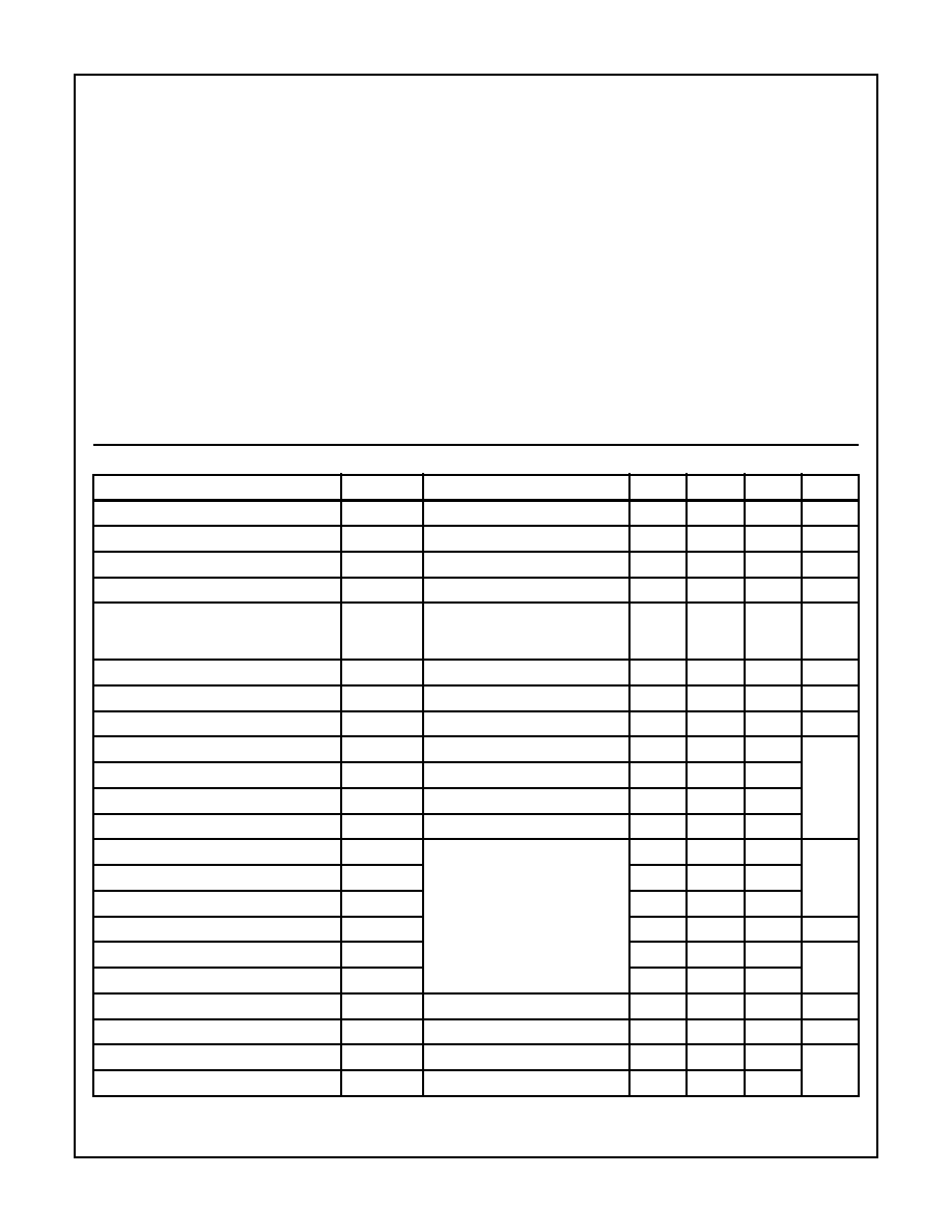
Absolute Maximum Ratings
T
C
= 25
o
C, Unless Otherwise Specified
FRX130D, R, H
UNITS
Drain to Source Voltage . . . . . . . . . . . . . . . . . . . . . . . . . . . . . . . . . . . . . . . . . . . . . . . . . . . . .V
DS
100
V
Drain to Gate Voltage (R
GS
= 20k
) . . . . . . . . . . . . . . . . . . . . . . . . . . . . . . . . . . . . . . . . . V
DGR
100
V
Continuous Drain Current. . . . . . . . . . . . . . . . . . . . . . . . . . . . . . . . . . . . . . . . . . . . . . . . . . . . . I
D
6
A
T
C
= 100
o
C . . . . . . . . . . . . . . . . . . . . . . . . . . . . . . . . . . . . . . . . . . . . . . . . . . . . . . . . . . . . . . I
D
4
A
Pulsed Drain Current . . . . . . . . . . . . . . . . . . . . . . . . . . . . . . . . . . . . . . . . . . . . . . . . . . . . . . . I
DM
18
A
Gate to Source Voltage . . . . . . . . . . . . . . . . . . . . . . . . . . . . . . . . . . . . . . . . . . . . . . . . . . . . .V
GS
±
20
V
Maximum Power Dissipation . . . . . . . . . . . . . . . . . . . . . . . . . . . . . . . . . . . . . . . . . . . . . . . . . . P
T
11.4
W
T
C
= 100
o
C . . . . . . . . . . . . . . . . . . . . . . . . . . . . . . . . . . . . . . . . . . . . . . . . . . . . . . . . . . . . . . P
T
4.5
W
Linear Derating Factor . . . . . . . . . . . . . . . . . . . . . . . . . . . . . . . . . . . . . . . . . . . . . . . . . . . . . . .
0.09
W/
o
C
Single Pulsed Avalanche Current, L = 100
µ
H, (See Test Figure). . . . . . . . . . . . . . . . . . . . . . I
AS
18
A
Continuous Source Current (Body Diode) . . . . . . . . . . . . . . . . . . . . . . . . . . . . . . . . . . . . . . . . I
S
6
A
Pulsed Source Current (Body Diode) . . . . . . . . . . . . . . . . . . . . . . . . . . . . . . . . . . . . . . . . . . . I
SM
18
A
Operating and Storage Temperature . . . . . . . . . . . . . . . . . . . . . . . . . . . . . . . . . . . . . .T
JC
, T
STG
-55 to 150
o
C
Lead Temperature (During Soldering) . . . . . . . . . . . . . . . . . . . . . . . . . . . . . . . . . . . . . . . . . . . T
L
(Distance >0.063in (1.6mm) from Case, 10s Max)
300
o
C
CAUTION: Stresses above those listed in "Absolute Maximum Ratings" may cause permanent damage to the device. This is a stress only rating and operation
of the device at these or any other conditions above those indicated in the operational sections of this specification is not implied.
Electrical Specifications
T
C
= 25
o
C, Unless Otherwise Specified
PARAMETER
SYMBOL
TEST CONDITIONS
MIN
TYP
MAX
UNITS
Drain to Source Breakdown Voltage
BV
DSS
I
D
= 1mA, V
GS
= 0V
100
-
-
V
Gate Threshold Voltage
V
GS(TH)
I
D
= 1mA, V
DS
= V
GS
2.0
4.0
V
Gate-Body Leakage Forward
I
GSSF
V
GS
= +20V
-
100
nA
Gate-Body Leakage Reverse
I
GSSR
V
GS
= -20V
-
100
nA
Zero Gate Voltage Drain Current
I
DSS1
I
DSS2
I
DSS3
V
DS
= 100V, V
GS
= 0
V
DS
= 80V, V
GS
= 0
V
DS
= 80V, V
GS
= 0, T
C
= 125
o
C
-
-
-
-
1
0.025
0.25
µ
A
Rated Avalanche Current
I
AR
Time = 20
µ
s
-
-
18
A
Drain to Source On-State Volts
V
DS(ON)
V
GS
= 10V, I
D
= 6A
-
-
1.130
V
Drain to Source On Resistance
r
DS(ON)
V
GS
= 10V, I
D
= 4A
-
-
0.180
Turn-On Delay Time
t
d(ON)
V
DD
= 50V, I
D
= 6A
-
-
30
ns
Rise Time
t
r
Pulse Width = 3
µ
s
-
-
100
Turn-Off Delay Time
t
d(OFF)
Period = 300
µ
s, Rg = 25
-
-
200
Fall Time
t
f
0
V
GS
10 (See Test Circuit)
-
-
100
Gate-Charge Threshold
Q
g(TH)
V
DD
= 50V, ID = 6A
I
GS1
= I
GS2
0
V
GS
20
1
-
4
nc
Gate-Charge On State
Q
g(ON)
17
-
70
Gate-Charge Total
Q
gM
32
-
128
Plateau Voltage
V
GP
3
-
12
V
Gate-Charge Source
Q
gS
3
-
14
nc
Gate-Charge Drain
Q
gD
8
-
32
Diode Forward Voltage
V
SD
I
D
= 6A, V
GD
= 0
0.6
-
1.8
V
Reverse Recovery Time
t
rr
I = 6A; di/dt = 100A/
µ
s
-
-
400
ns
Junction To Case
R
JC
-
-
11
o
C/W
Junction To Ambient
R
JA
Free Air Operation
-
-
250
FRX130D, FRX130R, FRX130H
3
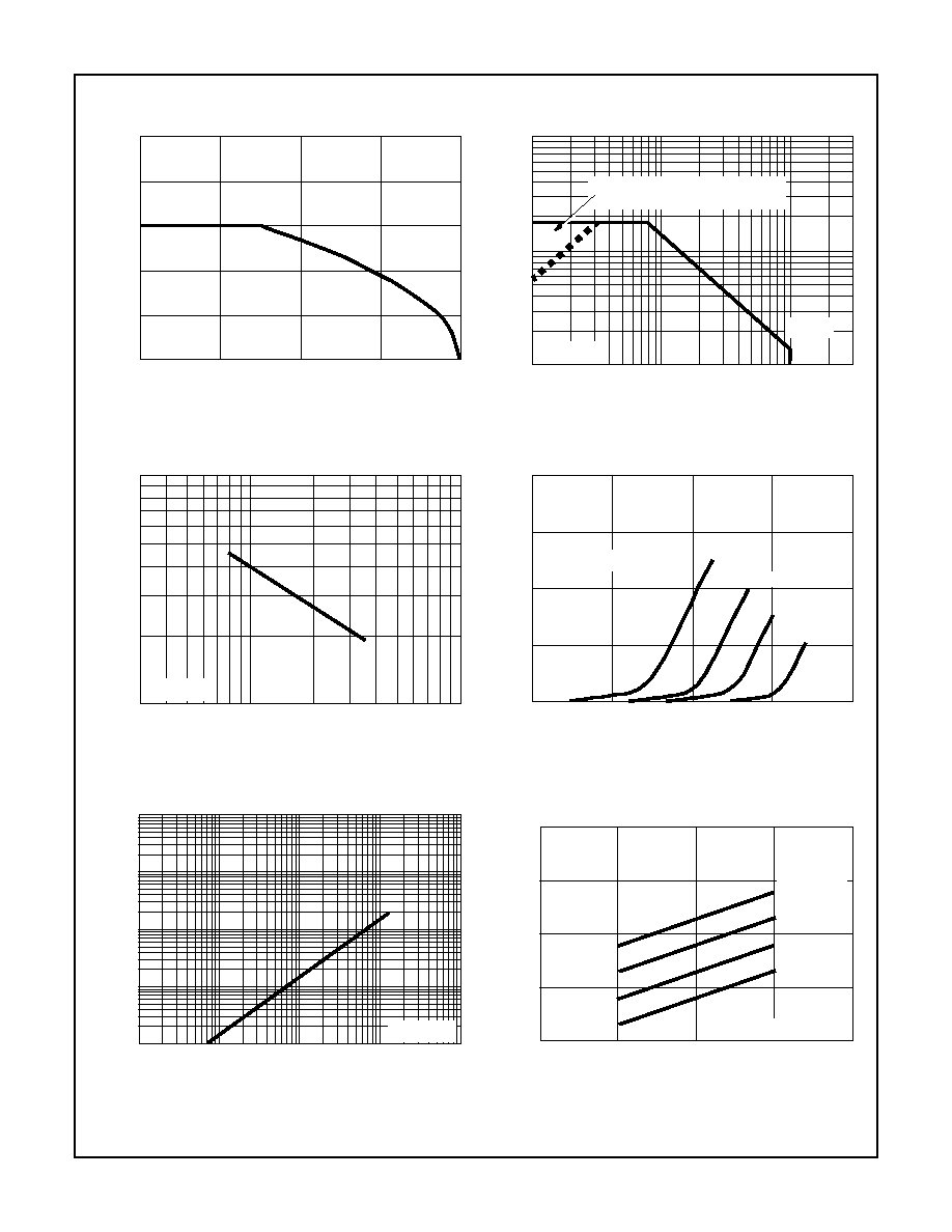
Typical Performance Curves
Unless Otherwise Specified
FIGURE 1. MAXIMUM CONTINUOUS DRAIN CURRENT vs
CASE TEMPERATURE
FIGURE 2. SAFE OPERATING AREA CURVE CASE
TEMPERATURE = 25
o
C
FIGURE 3. TYPICAL UNCLAMPED INDUCTIVE SWITCHING
FAILURE ONSET AVALANCHE MODE
FIGURE 4. NORMALIZED ON-RESISTANCE vs NEUTRON
FLUENCE N-CHANNEL
FIGURE 5. TYPICAL PHOTO CURRENT vs GAMMA RATE
FIGURE 6. DRAIN INDUCTANCE REQUIRED TO LIMIT GAMMA
DOT CURRENT TO I
LM
CASE TEMPERATURE (T
C
)
0
50
100
ID
, DRAIN (A)
FRX130
2
4
6
8
VDS DRAIN-TO-SOURCE (V)
50
100
ID
, DRAIN (A)
10
OPERATION IN THIS AREA
IS LIMITED BY r
DS(ON)
10ms
FRX130
TIME OF INDUCTIVE DISCHARGE (
µ
s)
100
500
ID
, DRAIN (A)
30
20
50
80
FRX130
1E13
1E14
1E15
FLUENCE - NEUTRONS/cm
2
4
3
2
NORMALIZED r
DS(ON)
50V
100V
500V
RATED BVDSS
200V
1E8
1E9
1E10
GAMMA DOT - RAD (Si)/s
100
10
1
DRAIN CURRENT (A)
FRX130
30
100
300
DRAIN SUPPLY (V)
1E-4
1E-5
1E-6
LIMITING INDUCT
ANCE (H)
ILM = 300A
ILM = 100A
ILM = 30A
ILM = 10A
GAMMA DOT
FRX130D, FRX130R, FRX130H
4
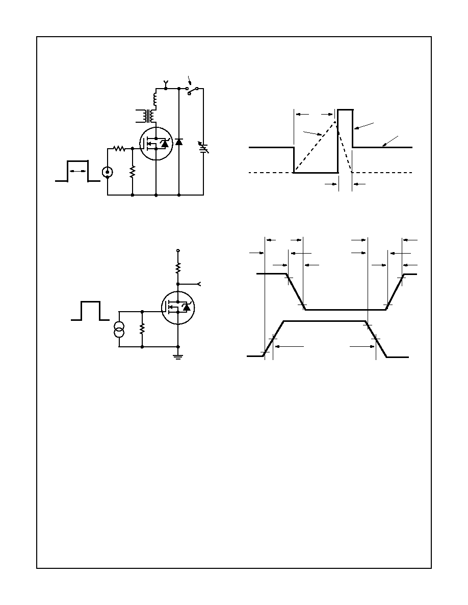
Test Circuits and Waveforms
FIGURE 7. UNCLAMPED ENERGY TEST CIRCUIT
FIGURE 8. UNCLAMPED ENERGY WAVEFORMS
FIGURE 9. RESISTIVE SWITCHING TEST CIRCUIT
FIGURE 10. RESISTIVE SWITCHING WAVEFORMS
t
P
V
GS
20V
L
+
-
V
DS
V
DD
DUT
VARY t
P
TO OBTAIN
REQUIRED PEAK I
AS
0V
50
50
50V-150V
I
AS
+
-
ELECTRONIC SWITCH OPENS
WHEN I
AS
IS REACHED
CURRENT
TRANSFORMER
V
DD
V
DS
BV
DSS
t
P
I
AS
t
AV
V
DS
DUT
R
GS
0V
V
GS
= 12V
V
DD
R
L
t
D(ON)
t
R
90%
10%
V
DS
90%
10%
t
F
t
D(OFF)
t
OFF
90%
50%
50%
10%
PULSE WIDTH
V
GS
t
ON
FRX130D, FRX130R, FRX130H
5
All Intersil semiconductor products are manufactured, assembled and tested under ISO9000 quality systems certification.
Intersil products are sold by description only. Intersil Corporation reserves the right to make changes in circuit design and/or specifications at any time without notice.
Accordingly, the reader is cautioned to verify that data sheets are current before placing orders. Information furnished by Intersil is believed to be accurate and reli-
able. However, no responsibility is assumed by Intersil or its subsidiaries for its use; nor for any infringements of patents or other rights of third parties which may
result from its use. No license is granted by implication or otherwise under any patent or patent rights of Intersil or its subsidiaries.
For information regarding Intersil Corporation and its products, see web site http://www.intersil.com
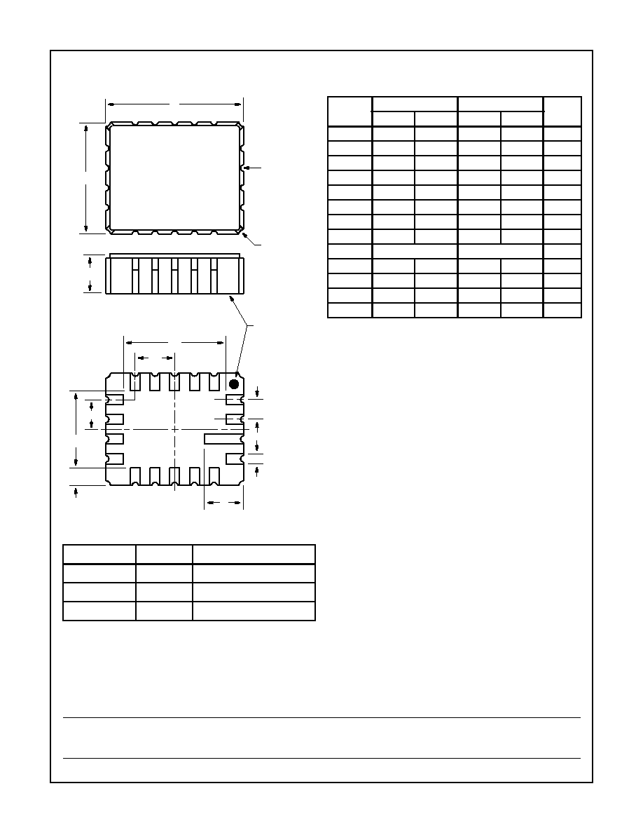
FRX130D, FRX130R, FRX130H
18 Pin CLCC
18 PIN CERAMIC LEADLESS CHIP CARRIER
ELEMENT
PAD
PINS CONNECTED
GATE
A
5
DRAIN
B
1, 2, 3, 4, 16, 17, 18
SOURCE
C
6, 7, 8, 9, 10, 11, 12, 13, 14, 15
E
D
R
1
R
A
D
2
D
1
E
2
E
1
e
b
L
1
2
L
1
SEATING
PLANE
SYMBOL
INCHES
MILLIMETERS
NOTES
MIN
MAX
MIN
MAX
A
0.092
0.112
2.34
2.84
-
b
0.020
0.030
0.51
0.76
-
D
0.275
0.295
6.99
7.49
-
D
1
0.175
0.215
4.45
5.46
-
D
2
0.070
0.080
1.78
2.03
-
E
0.340
0.360
8.64
9.14
-
E
1
0.240
0.280
6.10
7.11
-
E
2
0.095
0.105
2.42
2.66
-
e
0.050 BSC
1.27 BSC
-
L
0.085
0.115
2.16
2.92
-
L
1
0.035
0.055
0.89
1.39
-
R
0.007
0.017
0.18
0.43
4
R
1
0.003
0.013
0.08
0.33
4
NOTES:
1. No current JEDEC outline for this package.
2. All exposed metallized areas shall be plated with a minimum of 50
microinches of gold over nickel unless otherwise stated.
3. Metallized castellations shall be connected to the seating plane
and extend upward toward top of package.
4. Corner shape (notch, radius, square, etc.) may vary at the manu-
facturer's option.
5. Unless otherwise specified, a minimum clearance of 0.010 inches
(0.25mm) shall be maintained between all metallized areas.
6. Controlling dimension: Inch.
7. Revision 1 dated 6-93.