 | ÐлекÑÑоннÑй компоненÑ: FSJ055R1 | СкаÑаÑÑ:  PDF PDF  ZIP ZIP |
Äîêóìåíòàöèÿ è îïèñàíèÿ www.docs.chipfind.ru
1
FSJ055D, FSJ055R
70A, 60V, 0.012 Ohm, Radiation Hardened,
SEGR Resistant, N-Channel Power
MOSFETs
The Discrete Products Operation of Intersil has developed a
series of Radiation Hardened MOSFETs specifically
designed for commercial and military space applications.
Enhanced Power MOSFET immunity to Single Event Effects
(SEE), Single Event Gate Rupture (SEGR) in particular, is
combined with 100K RADS of total dose hardness to provide
devices which are ideally suited to harsh space
environments. The dose rate and neutron tolerance
necessary for military applications have not been sacrificed.
The Intersil portfolio of SEGR resistant radiation hardened
MOSFETs includes N-Channel and P-Channel devices in a
variety of voltage, current and on-resistance ratings.
Numerous packaging options are also available.
This MOSFET is an enhancement-mode silicon-gate power
field-effect transistor of the vertical DMOS (VDMOS)
structure. It is specially designed and processed to be
radiation tolerant. The MOSFET is well suited for
applications exposed to radiation environments such as
switching regulation, switching converters, motor drives,
relay drivers and drivers for high-power bipolar switching
transistors requiring high speed and low gate drive power.
This type can be operated directly from integrated circuits.
Reliability screening is available as either commercial, TXV
equivalent of MIL-S-19500, or Space equivalent of
MIL-S-19500. Contact Intersil for any desired deviations
from the data sheet.
Features
· 70A, 60V, r
DS(ON)
= 0.012
· Total Dose
- Meets Pre-RAD Specifications to 100K RAD (Si)
· Single Event
- Safe Operating Area Curve for Single Event Effects
- SEE Immunity for LET of 36MeV/mg/cm
2
with
V
DS
up to 80% of Rated Breakdown and
V
GS
of 10V Off-Bias
· Dose Rate
- Typically Survives 3E9 RAD (Si)/s at 80% BV
DSS
- Typically Survives 2E12 if Current Limited to I
DM
· Photo Current
- 6.0nA Per-RAD(Si)/s Typically
· Neutron
- Maintain Pre-RAD Specifications for
3E13 Neutrons/cm
2
- Usable to 3E14 Neutrons/cm
2
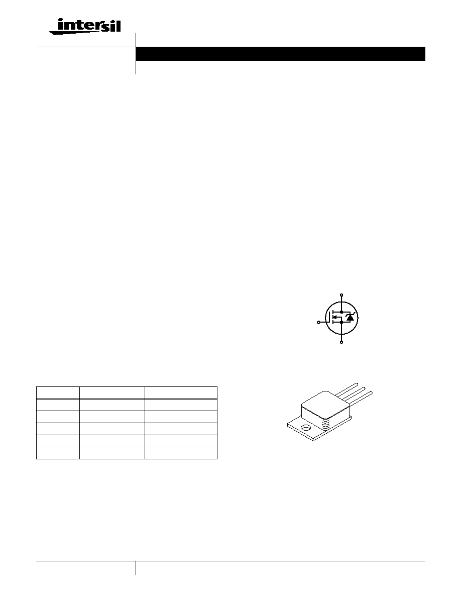
Symbol
Packaging
TO-254AA
Ordering Information
RAD LEVEL
SCREENING LEVEL
PART NUMBER/BRAND
10K
Commercial
FSJ055D1
10K
TXV
FSJ055D3
100K
Commercial
FSJ055R1
100K
TXV
FSJ055R3
100K
Space
FSJ055R4
D
G
S
CAUTION: Beryllia Warning per MIL-S-19500
refer to package specifications.
S
G
D
Data Sheet
October 1999
File Number
4250.5
CAUTION: These devices are sensitive to electrostatic discharge; follow proper IC Handling Procedures.
1-888-INTERSIL or 407-727-9207
|
Copyright
©
Intersil Corporation 1999
2
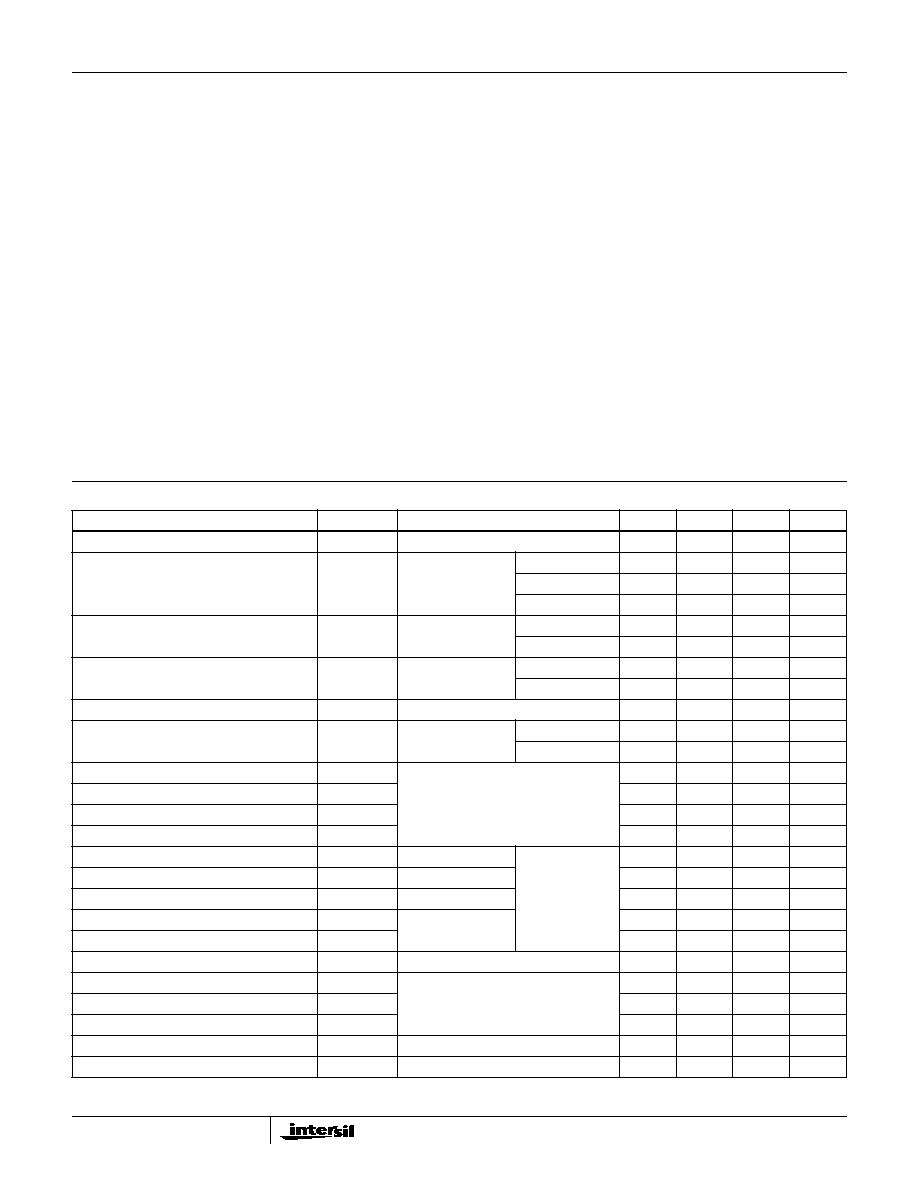
Absolute Maximum Ratings
T
C
= 25
o
C, Unless Otherwise Specified
FSJ055D, FSJ055R
UNITS
Drain to Source Voltage . . . . . . . . . . . . . . . . . . . . . . . . . . . . . . . . . . . . . . . . . . . . . . . . . . . . . . . .V
DS
60
V
Drain to Gate Voltage (R
GS
= 20k
) . . . . . . . . . . . . . . . . . . . . . . . . . . . . . . . . . . . . . . . . . . . . V
DGR
60
V
Continuous Drain Current
T
C
= 25
o
C . . . . . . . . . . . . . . . . . . . . . . . . . . . . . . . . . . . . . . . . . . . . . . . . . . . . . . . . . . . . . . . . . I
D
70
A
T
C
= 100
o
C . . . . . . . . . . . . . . . . . . . . . . . . . . . . . . . . . . . . . . . . . . . . . . . . . . . . . . . . . . . . . . . . I
D
54
A
Pulsed Drain Current . . . . . . . . . . . . . . . . . . . . . . . . . . . . . . . . . . . . . . . . . . . . . . . . . . . . . . . . . . I
DM
200
A
Gate to Source Voltage . . . . . . . . . . . . . . . . . . . . . . . . . . . . . . . . . . . . . . . . . . . . . . . . . . . . . . . .V
GS
±
20
V
Maximum Power Dissipation
T
C
= 25
o
C . . . . . . . . . . . . . . . . . . . . . . . . . . . . . . . . . . . . . . . . . . . . . . . . . . . . . . . . . . . . . . . . . P
T
125
W
T
C
= 100
o
C . . . . . . . . . . . . . . . . . . . . . . . . . . . . . . . . . . . . . . . . . . . . . . . . . . . . . . . . . . . . . . . . P
T
50
W
Linear Derating Factor . . . . . . . . . . . . . . . . . . . . . . . . . . . . . . . . . . . . . . . . . . . . . . . . . . . . . . . . . .
1.20
W/
o
C
Single Pulsed Avalanche Current, L = 100
µ
H, (See Test Figure) . . . . . . . . . . . . . . . . . . . . . . . . I
AS
200
A
Continuous Source Current (Body Diode) . . . . . . . . . . . . . . . . . . . . . . . . . . . . . . . . . . . . . . . . . . . I
S
70
A
Pulsed Source Current (Body Diode). . . . . . . . . . . . . . . . . . . . . . . . . . . . . . . . . . . . . . . . . . . . . . I
SM
200
A
Operating and Storage Temperature . . . . . . . . . . . . . . . . . . . . . . . . . . . . . . . . . . . . . . . . . .T
J
, T
STG
-55 to 150
o
C
Lead Temperature (During Soldering) . . . . . . . . . . . . . . . . . . . . . . . . . . . . . . . . . . . . . . . . . . . . . . T
L
(Distance >0.063 in. (1.6mm) from Case, 10s Max)
300
o
C
CAUTION: Stresses above those listed in "Absolute Maximum Ratings" may cause permanent damage to the device. This is a stress only rating and operation of the
device at these or any other conditions above those indicated in the operational sections of this specification is not implied.
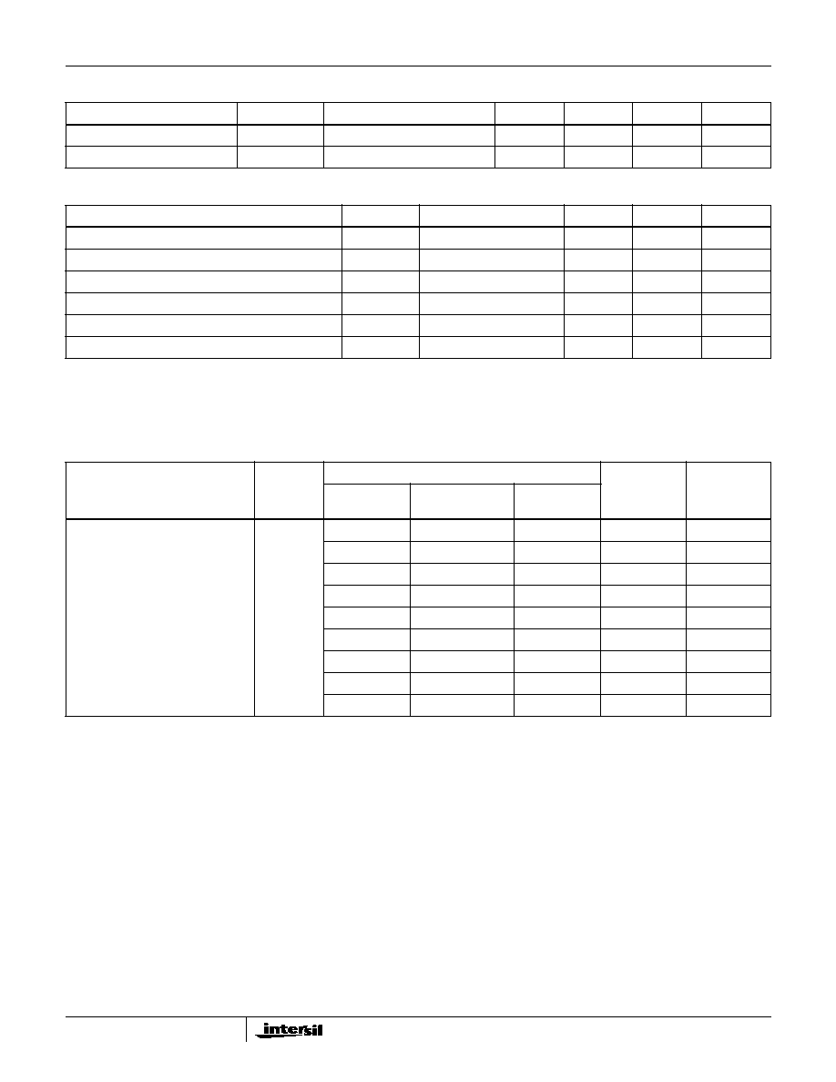
Electrical Specifications
T
C
= 25
o
C, Unless Otherwise Specified
PARAMETER
SYMBOL
TEST CONDITIONS
MIN
TYP
MAX
UNITS
Drain to Source Breakdown Voltage
BV
DSS
I
D
= 1mA, V
GS
= 0V
60
-
-
V
Gate Threshold Voltage
V
GS(TH)
V
GS
= V
DS
,
I
D
= 1mA
T
C
= -55
o
C
-
-
5.0
V
T
C
= 25
o
C
1.5
-
4.0
V
T
C
= 125
o
C
0.5
-
-
V
Zero Gate Voltage Drain Current
I
DSS
V
DS
= 48V,
V
GS
= 0V
T
C
= 25
o
C
-
-
25
µ
A
T
C
= 125
o
C
-
-
250
µ
A
Gate to Source Leakage Current
I
GSS
V
GS
=
±
20V
T
C
= 25
o
C
-
-
100
nA
T
C
= 125
o
C
-
-
200
nA
Drain to Source On-State Voltage
V
DS(ON)
V
GS
= 12V, I
D
= 70A
-
-
0.88
V
Drain to Source On Resistance
r
DS(ON)12
I
D
= 54A,
V
GS
= 12V
T
C
= 25
o
C
-
0.008
0.012
T
C
= 125
o
C
-
-
0.022
Turn-On Delay Time
t
D(ON)
V
DD
= 30V, I
D
= 70A,
R
L
= 0.43
, V
GS
12V,
R
GS
= 2.35
-
-
40
ns
Rise Time
t
r
-
-
200
ns
Turn-Off Delay Time
t
d(OFF)
-
-
70
ns
Fall Time
t
f
-
-
40
ns
Total Gate Charge
Q
g(TOT)
V
GS
= 0V to 20V
V
DD
= 30V,
I
D
= 70A
-
-
280
nC
Gate Charge at 12V
Q
g(12)
V
GS
= 0V to 12V
-
150
170
nC
Threshold Gate Charge
Q
g(TH)
V
GS
= 0V to 2V
-
-
12
nC
Gate Charge Source
Q
gs
-
35
43
nC
Gate Charge Drain
Q
gd
-
59
81
nC
Plateau Voltage
V
(PLATEAU)
I
D
= 70A, V
DS
= 15V
-
7
-
V
Input Capacitance
C
ISS
V
DS
= 25V, V
GS
= 0V,
f = 1MHz
-
4850
-
pF
Output Capacitance
C
OSS
-
2200
-
pF
Reverse Transfer Capacitance
C
RSS
-
425
-
pF
Thermal Resistance Junction to Case
R
JC
-
-
0.83
o
C/W
Thermal Resistance Junction to Ambient
R
JA
-
-
40
o
C/W
FSJ055D, FSJ055R
3
Source to Drain Diode Specifications
PARAMETER
SYMBOL
TEST CONDITIONS
MIN
TYP
MAX
UNITS
Forward Voltage
V
SD
I
SD
= 70A
0.6
-
1.8
V
Reverse Recovery Time
t
rr
I
SD
= 70A, dI
SD
/dt = 100A/
µ
s
-
-
250
ns
Electrical Specifications up to 100K RAD
T
C
= 25
o
C, Unless Otherwise Specified
PARAMETER
SYMBOL
TEST CONDITIONS
MIN
MAX
UNITS
Drain to Source Breakdown Volts
(Note 3)
BV
DSS
V
GS
= 0, I
D
= 1mA
60
-
V
Gate to Source Threshold Volts
(Note 3)
V
GS(TH)
V
GS
= V
DS
, I
D
= 1mA
1.5
4.0
V
Gate to Body Leakage
(Notes 2, 3)
I
GSS
V
GS
=
±
20V, V
DS
= 0V
-
100
nA
Zero Gate Leakage
(Note 3)
I
DSS
V
GS
= 0, V
DS
= 48V
-
25
µ
A
Drain to Source On-State Volts
(Notes 1, 3)
V
DS(ON)
V
GS
= 12V, I
D
= 70A
-
0.88
V
Drain to Source On Resistance
(Notes 1, 3)
r
DS(ON)12
V
GS
= 12V, I
D
= 54A
-
0.012
NOTES:
1. Pulse test, 300
µ
s Max.
2. Absolute value.
3. Insitu Gamma bias must be sampled for both V
GS
= 12V, V
DS
= 0V and V
GS
= 0V, V
DS
= 80% BV
DSS
.
Single Event Effects (SEB, SEGR)
(Note 4)
TEST
SYMBOL
ENVIRONMENT (NOTE 5)
APPLIED V
GS
BIAS (V)
(NOTE 6)
MAXIMUM
V
DS
BIAS (V)
ION
SPECIES
TYPICAL LET
(MeV/mg/cm)
TYPICAL
RANGE (
µ
)
Single Event Effects Safe
Operating Area
SEESOA
Ni
26
43
-20
60
Br
37
36
-10
60
Br
37
36
-15
48
Br
37
36
-20
36
I
60
31
0
60
I
60
31
-5
48
I
60
31
-10
36
I
60
31
-15
24
I
60
31
-20
12
NOTES:
4. Testing conducted at Brookhaven National Labs; sponsored by Naval Surface Warfare Center (NSWC), Crane, IN.
5. Fluence = 1E5 ions/cm
2
(typical), T = 25
o
C.
6. Does not exhibit Single Event Burnout (SEB) or Single Event Gate Rupture (SEGR).
FSJ055D, FSJ055R
4
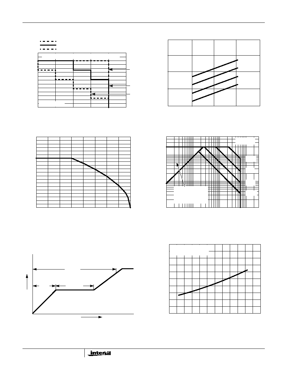
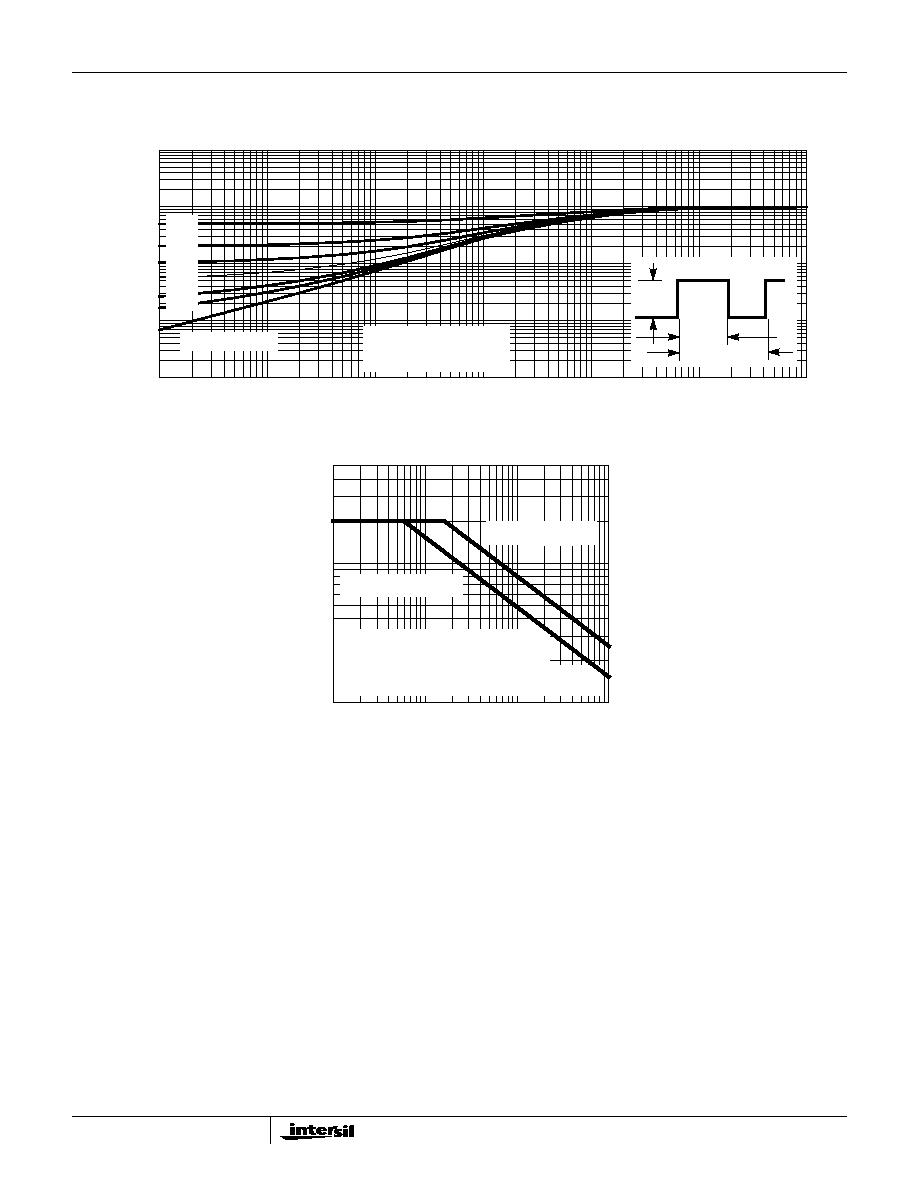
Typical Performance Curves
FIGURE 1. SINGLE EVENT EFFECTS SAFE OPERATING AREA
FIGURE 2. DRAIN INDUCTANCE REQUIRED TO LIMIT
GAMMA DOT CURRENT TO I
AS
FIGURE 3. MAXIMUM CONTINUOUS DRAIN CURRENT vs
TEMPERATURE
FIGURE 4. FORWARD BIAS SAFE OPERATING AREA
FIGURE 5. BASIC GATE CHARGE WAVEFORM
FIGURE 6. NORMALIZED r
DS(ON)
vs JUNCTION TEMPERATURE
LET = 37MeV/mg/cm
2
, RANGE = 36
µ
LET = 26MeV/mg/cm
2
, RANGE = 43
µ
LET = 60MeV/mg/cm
2
, RANGE = 31
µ
40
0
0
-10
-15
-20
-25
-5
V
GS
(V)
V
DS
(V)
10
20
30
50
60
70
TEMP = 25
o
C
FLUENCE = 1E5 IONS/cm
2
(TYPICAL)
1
2
3
1 -
2 -
3 -
300
100
10
LIMITING INDUCT
ANCE (HENR
Y)
DRAIN SUPPLY (V)
1000
ILM = 10A
300A
1E
-4
1E
-5
1E
-6
30
100A
30A
1E
-7
1E
-3
I
D
, DRAIN (A)
T
C
, CASE TEMPERATURE (
o
C)
150
100
50
0
-50
0
20
40
30
10
100
90
80
70
60
50
100
10
1
1
I
D
, DRAIN CURRENT (A)
V
DS
, DRAIN TO SOURCE VOLTAGE (V)
10
100
0.1
300
500
OPERATION IN THIS
AREA MAY BE
LIMITED BY r
DS(ON)
100ms
1ms
100
µ
s
10ms
T
C
= 25
o
C
CHARGE
Q
GD
Q
G
V
G
Q
GS
12V
2.5
2.0
1.5
1.0
0.5
0.0
-80
-40
0
40
80
120
160
T
J
, JUNCTION TEMPERATURE (
o
C)
r
DS(ON)
, NORMALIZED DRAIN T
O
SOURCE
ON RESIST
ANCE
250ms PULSE TEST
V
GS
= 12V, I
D
= 54A
FSJ055D, FSJ055R
5
FIGURE 7. NORMALIZED MAXIMUM TRANSIENT THERMAL RESPONSE
FIGURE 8. UNCLAMPED INDUCTIVE SWITCHING
Typical Performance Curves
(Continued)
NORMALIZED
1
0.1
0.01
10
-5
10
-4
10
-3
10
-2
10
-1
10
0
10
1
t, RECTANGULAR PULSE DURATION (s)
THERMAL RESPONSE (Z
JC
)
0.001
10
P
DM
t
1
t
2
NOTES:
DUTY FACTOR: D = t
1
/t
2
PEAK T
J
= P
DM
x Z
JC
+ T
C
SINGLE PULSE
0.05
0.5
0.02
0.1
0.01
0.2
100
10
0.01
0.1
1
t
AV
, TIME IN AVALANCHE (ms)
I
AS
,
A
V
ALANCHE CURRENT (A)
10
500
STARTING T
J
= 25
o
C
STARTING T
J
= 150
o
C
t
AV
= (L) (I
AS
) / (1.3 RATED BV
DSS
- V
DD
)
IF R = 0
IF R
0
t
AV
= (L/R) ln [(I
AS
*R) / (1.3 RATED BV
DSS
- V
DD
) + 1]
FSJ055D, FSJ055R