1
TM
File Number
4756.1
CAUTION: These devices are sensitive to electrostatic discharge; follow proper ESD Handling Procedures.
1-888-INTERSIL or 321-724-7143
|
Intersil and Design is a trademark of Intersil Corporation.
|
Copyright
©
Intersil Corporation 2000
FSTJ9055D, FSTJ9055R
Radiation Hardened, SEGR Resistant
P-Channel Power MOSFETs
The Discrete Products Operation of Intersil has developed a
series of Radiation Hardened MOSFETs specifically
designed for commercial and military space applications.
Immunity to Single Event Effects (SEE) is combined with
100K RADs of total dose hardness to provide devices which
are ideally suited to harsh space environments. The dose
rate and neutron tolerance necessary for military
applications have not been sacrificed.
The Intersil portfolio of SEGR resistant radiation hardened
MOSFETs includes N-Channel and P-Channel devices in a
variety of voltage, current and on-resistance ratings.
Numerous packaging options are also available.
This MOSFET is an enhancement-mode silicon-gate power
field-effect transistor of the vertical DMOS (VDMOS)
structure. It is specially designed and processed to be
radiation tolerant. The MOSFET is well suited for
applications exposed to radiation environments such as
switching regulation, switching converters, motor drives,
relay drivers and drivers for high-power bipolar switching
transistors requiring high speed and low gate drive power.
This type can be operated directly from integrated circuits.
Reliability screening is available as either commercial, TXV
equivalent of MIL-S-19500, or Space equivalent of
MIL-S-19500. Contact Intersil for any desired deviations
from the data sheet.
Formerly available as type TA17750T.
Features
∑ 62A, -60V, r
DS(ON)
= 0.023
∑ Total Dose
- Meets Pre-RAD Specifications to 100K RAD (Si)
∑ Single Event
- Safe Operating Area Curve for Single Event Effects
- SEE Immunity for LET of 36MeV/mg/cm
2
with
V
DS
up to 80% of Rated Breakdown and
V
GS
of 10V Off-Bias
∑ Dose Rate
- Typically Survives 3E9 RAD (Si)/s at 80% BV
DSS
- Typically Survives 2E12 if Current Limited to I
DM
∑ Photo Current
- 6nA Per-RAD(Si)/s Typically
∑ Neutron
- Maintain Pre-RAD Specifications for 3E13
Neutrons/cm
2
- Usable to 3E14 Neutrons/cm
2
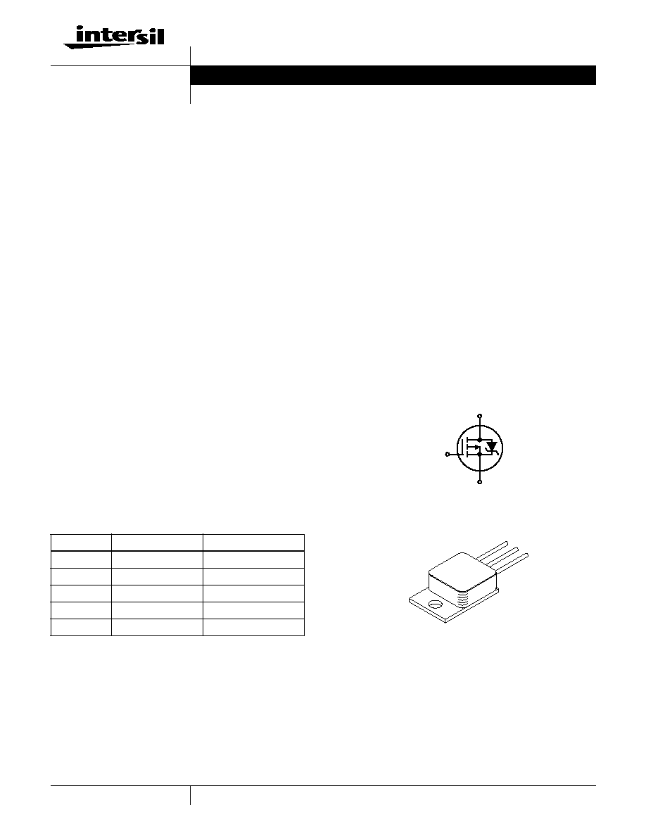
Symbol
Packaging
TO-254AA
Ordering Information
RAD LEVEL
SCREENING LEVEL
PART NUMBER/BRAND
10K
Commercial
FSTJ9055D1
10K
TXV
FSTJ9055D3
100K
Commercial
FSTJ9055R1
100K
TXV
FSTJ9055R3
100K
Space
FSTJ9055R4
G
D
S
CAUTION: Beryllia Warning per MIL-S-19500
refer to package specifications.
Data Sheet
June 2000
2
Absolute Maximum Ratings
T
C
= 25
o
C, Unless Otherwise Specified
FSTJ9055D, FSTJ9055R
UNITS
Drain to Source Voltage . . . . . . . . . . . . . . . . . . . . . . . . . . . . . . . . . . . . . . . . . . . . . . . . . . . . . . . .V
DS
-60
V
Drain to Gate Voltage (R
GS
= 20k
) . . . . . . . . . . . . . . . . . . . . . . . . . . . . . . . . . . . . . . . . . . . . V
DGR
-60
V
Continuous Drain Current
T
C
= 25
o
C . . . . . . . . . . . . . . . . . . . . . . . . . . . . . . . . . . . . . . . . . . . . . . . . . . . . . . . . . . . . . . . . . I
D
62
A
T
C
= 100
o
C . . . . . . . . . . . . . . . . . . . . . . . . . . . . . . . . . . . . . . . . . . . . . . . . . . . . . . . . . . . . . . . . I
D
39
A
Pulsed Drain Current . . . . . . . . . . . . . . . . . . . . . . . . . . . . . . . . . . . . . . . . . . . . . . . . . . . . . . . . . . I
DM
186
A
Gate to Source Voltage . . . . . . . . . . . . . . . . . . . . . . . . . . . . . . . . . . . . . . . . . . . . . . . . . . . . . . . .V
GS
±
20
V
Maximum Power Dissipation
T
C
= 25
o
C . . . . . . . . . . . . . . . . . . . . . . . . . . . . . . . . . . . . . . . . . . . . . . . . . . . . . . . . . . . . . . . . . P
T
125
W
T
C
= 100
o
C . . . . . . . . . . . . . . . . . . . . . . . . . . . . . . . . . . . . . . . . . . . . . . . . . . . . . . . . . . . . . . . . P
T
50
W
Linear Derating Factor . . . . . . . . . . . . . . . . . . . . . . . . . . . . . . . . . . . . . . . . . . . . . . . . . . . . . . . . . .
1.20
W/
o
C
Single Pulsed Avalanche Current, L = 100
µ
H, (See Test Figure) . . . . . . . . . . . . . . . . . . . . . . . . I
AS
186
A
Continuous Source Current (Body Diode) . . . . . . . . . . . . . . . . . . . . . . . . . . . . . . . . . . . . . . . . . . . I
S
62
A
Pulsed Source Current (Body Diode). . . . . . . . . . . . . . . . . . . . . . . . . . . . . . . . . . . . . . . . . . . . . . I
SM
186
A
Operating and Storage Temperature . . . . . . . . . . . . . . . . . . . . . . . . . . . . . . . . . . . . . . . . . . T
J
, T
STG
-55 to 150
o
C
Lead Temperature (During Soldering) . . . . . . . . . . . . . . . . . . . . . . . . . . . . . . . . . . . . . . . . . . . . . . T
L
(Distance >0.063in (1.6mm) from Case, 10s Max)
300
o
C
CAUTION: Stresses above those listed in "Absolute Maximum Ratings" may cause permanent damage to the device. This is a stress only rating and operation of the
device at these or any other conditions above those indicated in the operational sections of this specification is not implied.
Electrical Specifications
T
C
= 25
o
C, Unless Otherwise Specified
PARAMETER
SYMBOL
TEST CONDITIONS
MIN
TYP
MAX
UNITS
Drain to Source Breakdown Voltage
BV
DSS
I
D
= 1mA, V
GS
= 0V
-60
-
-
V
Gate Threshold Voltage
V
GS(TH)
V
GS
= V
DS
,
I
D
= 1mA
T
C
= -55
o
C
-
-
-7.0
V
T
C
= 25
o
C
-2.0
-
-6.0
V
T
C
= 125
o
C
-1.0
-
-
V
Zero Gate Voltage Drain Current
I
DSS
V
DS
= -48V,
V
GS
= 0V
T
C
= 25
o
C
-
-
25
µ
A
T
C
= 125
o
C
-
-
250
µ
A
Gate to Source Leakage Current
I
GSS
V
GS
=
±
20V
T
C
= 25
o
C
-
-
100
nA
T
C
= 125
o
C
-
200
nA
Drain to Source On-State Voltage
V
DS(ON)
V
GS
= -12V, I
D
= 62A
-
-
-1.55
V
Drain to Source On Resistance
r
DS(ON)12
I
D
= 39A,
V
GS
= -12V
T
C
= 25
o
C
-
0.016
0.023
T
C
= 125
o
C
-
-
0.035
Turn-On Delay Time
t
d(ON)
V
DD
= -30V, I
D
= 62A,
R
L
= 0.48
, V
GS
= -12V,
R
GS
= 2.35
-
-
50
ns
Rise Time
t
r
-
-
120
ns
Turn-Off Delay Time
t
d(OFF)
-
-
100
ns
Fall Time
t
f
-
-
40
ns
Total Gate Charge
Q
g(TOT)
V
GS
= 0V to -20V
V
DD
= -30V,
I
D
= 62A
-
-
330
nC
Gate Charge at 12V
Q
g(12)
V
GS
= 0V to -12V
-
160
190
nC
Threshold Gate Charge
Q
g(TH)
V
GS
= 0V to -2V
-
-
18
nC
Gate Charge Source
Q
gs
-
51
71
nC
Gate Charge Drain
Q
gd
-
31
46
nC
Plateau Voltage
V
(PLATEAU)
I
D
= 62A, V
DS
= -15V
-
-6
-
V
Input Capacitance
C
ISS
V
DS
= -25V, V
GS
= 0V,
f = 1MHz
-
7100
-
pF
Output Capacitance
C
OSS
-
2130
-
pF
Reverse Transfer Capacitance
C
RSS
-
370
-
pF
Thermal Resistance Junction to Case
R
JC
-
-
0.83
o
C/W
FSTJ9055D, FSTJ9055R

3
Source to Drain Diode Specifications
PARAMETER
SYMBOL
TEST CONDITIONS
MIN
TYP
MAX
UNITS
Forward Voltage
V
SD
I
SD
= 62A
-0.6
-
-1.8
V
Reverse Recovery Time
t
rr
I
SD
= 59A, dI
SD
/dt = 100A/
µ
s
-
-
110
ns
Electrical Specifications up to 100K RAD
T
C
= 25
o
C, Unless Otherwise Specified
PARAMETER
SYMBOL
TEST CONDITIONS
MIN
MAX
UNITS
Drain to Source Breakdown Volts
(Note 3)
BV
DSS
V
GS
= 0, I
D
= 1mA
-60
-
V
Gate to Source Threshold Volts
(Note 3)
V
GS(TH)
V
GS
= V
DS
, I
D
= 1mA
-2.0
-6.0
V
Gate to Body Leakage
(Notes 2, 3)
I
GSS
V
GS
=
±
20V, V
DS
= 0V
-
100
nA
Zero Gate Leakage
(Note 3)
I
DSS
V
GS
= 0, V
DS
= -48V
-
25
µ
A
Drain to Source On-State Volts
(Notes 1, 3)
V
DS(ON)
V
GS
= -12V, I
D
= 62A
-
-1.55
V
Drain to Source On Resistance
(Notes 1, 3)
r
DS(ON)12
V
GS
= -12V, I
D
= 39A
-
0.023
NOTES:
1. Pulse test, 300
µ
s Max.
2. Absolute value.
3. Insitu Gamma bias must be sampled for both V
GS
= -12V, V
DS
= 0V and V
GS
= 0V, V
DS
= 80% BV
DSS
.
Single Event Effects (SEB, SEGR)
Note 4
TEST
SYMBOL
ENVIRONMENT (NOTE 5)
APPLIED
V
GS
BIAS
(V)
(NOTE 6)
MAXIMUM
V
DS
BIAS (V)
ION
SPECIES
TYPICAL LET
(MeV/mg/cm)
TYPICAL
RANGE (
µ
)
Single Event Effects Safe Operating Area
SEESOA
Ni
26
43
20
-60
Br
37
36
10
-60
Br
37
36
15
-36
Br
37
36
20
-24
NOTES:
4. Testing conducted at Brookhaven National Labs; witnessed by Naval Surface Warfare Center (NSWC), Crane, IN.
5. Fluence = 1E5 ions/cm
2
(typical), T
C
= 25
o
C.
6. Does not exhibit Single Event Burnout (SEB) or Single Event Gate Rupture (SEGR).
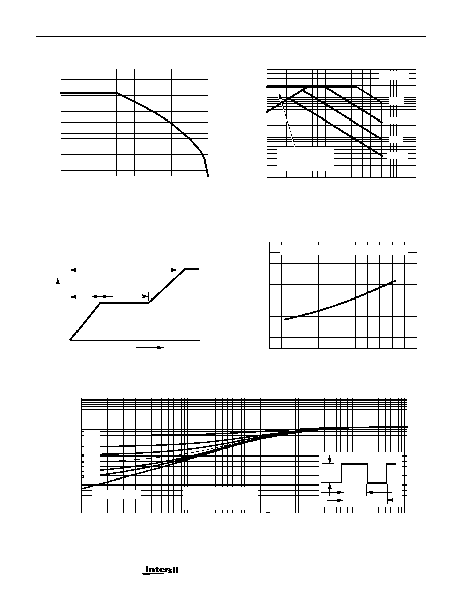
Typical Performance Curves
Unless Otherwise Specified
FIGURE 1. SINGLE EVENT EFFECTS SAFE OPERATING
AREA
FIGURE 2. DRAIN INDUCTANCE REQUIRED TO LIMIT
GAMMA DOT CURRENT TO I
AS
-40
0
0
10
15
20
25
5
V
GS
(V)
V
DS
(V)
-10
-20
-30
-50
-60
-70
LET = 37MeV/mg/cm
2
, RANGE = 36m
LET = 26MeV/mg/cm
2
, RANGE = 43m
FLUENCE = 1E5 IONS/cm
2
(TYPICAL)
TEMP = 25
o
C
-300
-100
-10
LIMITING INDUCT
ANCE (HENR
Y)
DRAIN SUPPLY (V)
-1000
ILM = 10A
300A
1E-4
1E-5
1E-6
-30
100A
30A
1E-7
1E-3
FSTJ9055D, FSTJ9055R
4
FIGURE 3. MAXIMUM CONTINUOUS DRAIN CURRENT vs
TEMPERATURE
FIGURE 4. FORWARD BIAS SAFE OPERATING AREA
FIGURE 5. BASIC GATE CHARGE WAVEFORM
FIGURE 6. NORMALIZED r
DS(ON)
vs JUNCTION TEMPERATURE
FIGURE 7. NORMALIZED MAXIMUM TRANSIENT THERMAL RESPONSE
Typical Performance Curves
Unless Otherwise Specified (Continued)
I
D
, DRAIN (A)
T
C
, CASE TEMPERATURE (
o
C)
150
100
50
0
-50
0
20
40
80
60
100
10
1
-1
V
DS
, DRAIN TO SOURCE VOLTAGE (V)
-10
-100
-200
I
D
,
DRAIN CURRENT (A)
500
100
µ
s
1ms
10ms
OPERATION IN THIS
AREA MAY BE
LIMITED BY r
DS(ON)
T
C
= 25
o
C
100ms
CHARGE
Q
GD
Q
G
V
G
Q
GS
-12V
2.5
2.0
1.5
1.0
0.5
0.0
-80
-40
0
40
80
120
160
T
J
, JUNCTION TEMPERATURE (
o
C)
NORMALIZED r
DS(ON)
PULSE DURATION = 250ms, V
GS
= -12V, I
D
= 39A
NORMALIZED
1
0.1
0.01
10
-5
10
-4
10
-3
10
-2
10
-1
10
0
10
1
t, RECTANGULAR PULSE DURATION (s)
THERMAL RESPONSE (Z
JC
)
0.001
10
P
DM
t
1
t
2
NOTES:
DUTY FACTOR: D = t
1
/t
2
PEAK T
J
= P
DM
x Z
JC
+ T
C
SINGLE PULSE
0.05
0.5
0.02
0.1
0.01
0.2
FSTJ9055D, FSTJ9055R

5
FIGURE 8. UNCLAMPED INDUCTIVE SWITCHING
Typical Performance Curves
Unless Otherwise Specified (Continued)
100
10
0.1
1
t
AV
, TIME IN AVALANCHE (ms)
I
AS
,
A
V
ALANCHE CURRENT (A)
10
STARTING T
J
= 150
o
C
STARTING T
J
= 25
o
C
t
AV
= (L/R) ln [(I
AS
*R) / (1.3 RATED BV
DSS
- V
DD
) + 1]
IF R = 0
t
AV
= (L) (I
AS
) / (1.3 RATED BV
DSS
- V
DD
)
IF R
0
500
Test Circuits and Waveforms
FIGURE 9. UNCLAMPED ENERGY TEST CIRCUIT
FIGURE 10. UNCLAMPED ENERGY WAVEFORMS
FIGURE 11. RESISTIVE SWITCHING TEST CIRCUIT
FIGURE 12. RESISTIVE SWITCHING WAVEFORMS
t
P
V
GS
20V
L
+
-
V
DS
V
DD
DUT
VARY t
P
TO OBTAIN
REQUIRED PEAK I
AS
0V
50
50
50V-150V
I
AS
+
-
ELECTRONIC SWITCH OPENS
WHEN I
AS
IS REACHED
CURRENT
TRANSFORMER
V
DD
V
DS
BV
DSS
t
P
I
AS
t
AV
V
DD
R
L
V
DS
DUT
R
GS
0V
V
GS
= -12V
t
d(ON)
t
r
90%
10%
V
DS
90%
10%
t
f
t
d(OFF)
t
OFF
90%
50%
50%
10%
PULSE WIDTH
V
GS
t
ON
FSTJ9055D, FSTJ9055R
6
Screening Information
Screening is performed in accordance with the latest revision in effect of MIL-S-19500, (Screening Information Table).
Delta Tests and Limits (JANTXV Equivalent, JANS Equivalent)
T
C
= 25
o
C, Unless Otherwise Specified
PARAMETER
SYMBOL
TEST CONDITIONS
MAX
UNITS
Gate to Source Leakage Current
I
GSS
V
GS
=
±
20V
±
20 (Note 7)
nA
Zero Gate Voltage Drain Current
I
DSS
V
DS
= 80% Rated Value
±
25 (Note 7)
µ
A
Drain to Source On Resistance
r
DS(ON)
T
C
= 125
o
C at Rated I
D
±
20% (Note 8)
Gate Threshold Voltage
V
GS(TH)
I
D
= 1.0mA
±
20% (Note 8)
V
NOTES:
7. Or 100% of Initial Reading (whichever is greater).
8. Of Initial Reading.
Screening Information
TEST
JANTXV EQUIVALENT
JANS EQUIVALENT
Gate Stress
V
GS
= -30V, t = 250
µ
s
V
GS
= -30V, t = 250
µ
s
Pind
Optional
Required
Pre Burn-In Tests (Note 9)
MIL-S-19500 Group A,
Subgroup 2 (All Static Tests at 25
o
C)
MIL-S-19500 Group A,
Subgroup 2 (All Static Tests at 25
o
C)
Steady State Gate
Bias (Gate Stress)
MIL-STD-750, Method 1042, Condition B
V
GS
= 80% of Rated Value,
T
A
= 150
o
C, Time = 48 hours
MIL-STD-750, Method 1042, Condition B
V
GS
= 80% of Rated Value,
T
A
= 150
o
C, Time = 48 hours
Interim Electrical Tests (Note 9)
All Delta Parameters Listed in the Delta Tests
and Limits Table
All Delta Parameters Listed in the Delta Tests
and Limits Table
Steady State Reverse
Bias (Drain Stress)
MIL-STD-750, Method 1042, Condition A
V
DS
= 80% of Rated Value,
T
A
= 150
o
C, Time = 160 hours
MIL-STD-750, Method 1042, Condition A
V
DS
= 80% of Rated Value,
T
A
= 150
o
C, Time = 240 hours
PDA
10%
5%
Final Electrical Tests (Note 9)
MIL-S-19500, Group A, Subgroup 2
MIL-S-19500, Group A,
Subgroups 2 and 3
NOTE:
9. Test limits are identical pre and post burn-in.
Additional Screening Tests
PARAMETER
SYMBOL
TEST CONDITIONS
MAX
UNITS
Safe Operating Area
SOA
V
DS
= -48V, t = 10ms
11
A
Unclamped Inductive Switching
I
AS
V
GS(PEAK)
= -15V, L = 0.1mH
186
A
Thermal Response
V
SD
t
H
= 100ms; V
H
= -25V; I
H
= 4A
120
mV
Thermal Impedance
V
SD
t
H
= 500ms; V
H
= -20V; I
H
= 4A
190
mV
FSTJ9055D, FSTJ9055R

7
Rad Hard Data Packages - Intersil Power Transistors
TXV Equivalent
1. RAD HARD TXV EQUIVALENT - STANDARD DATA
PACKAGE
A. Certificate of Compliance
B. Assembly Flow Chart
C. Preconditioning Attributes Data Sheet
D. Group A
Attributes Data Sheet
E. Group B
Attributes Data Sheet
F. Group C
Attributes Data Sheet
G. Group D
Attributes Data Sheet
2. RAD HARD TXV EQUIVALENT - OPTIONAL DATA
PACKAGE
A. Certificate of Compliance
B. Assembly Flow Chart
C. Preconditioning - Attributes Data Sheet
- Pre and Post Burn-In Read and Record
Data
D. Group A
- Attributes Data Sheet
E. Group B
- Attributes Data Sheet
- Pre and Post Read and Record Data for
Intermittent Operating Life (Subgroup B3)
- Bond Strength Data (Subgroup B3)
- Pre and Post High Temperature Operating
Life Read and Record Data (Subgroup B6)
F. Group C
- Attributes Data Sheet
- Pre and Post Read and Record Data for
Intermittent Operating Life (Subgroup C6)
- Bond Strength Data (Subgroup C6)
G. Group D
- Attributes Data Sheet
- Pre and Post RAD Read and Record Data
Class S - Equivalents
1. RAD HARD "S" EQUIVALENT - STANDARD DATA
PACKAGE
A. Certificate of Compliance
B. Serialization Records
C. Assembly Flow Chart
D. SEM Photos and Report
E. Preconditioning - Attributes Data Sheet
- HTRB - Hi Temp Gate Stress Post
Reverse Bias Data and Delta Data
- HTRB - Hi Temp Drain Stress Post
Reverse Bias Delta Data
F. Group A
- Attributes Data Sheet
G. Group B
- Attributes Data Sheet
H. Group C
- Attributes Data Sheet
I. Group D
- Attributes Data Sheet
2. RAD HARD MAX. "S" EQUIVALENT - OPTIONAL
DATA PACKAGE
A. Certificate of Compliance
B. Serialization Records
C. Assembly Flow Chart
D. SEM Photos and Report
E. Preconditioning - Attributes Data Sheet
- HTRB - Hi Temp Gate Stress Post
Reverse Bias Data and Delta Data
- HTRB - Hi Temp Drain Stress Post
Reverse Bias Delta Data
- X-Ray and X-Ray Report
F. Group A
- Attributes Data Sheet
- Subgroups A2, A3, A4, A5 and A7 Data
G. Group B
- Attributes Data Sheet
- Subgroups B1, B3, B4, B5 and B6 Data
H. Group C
- Attributes Data Sheet
- Subgroups C1, C2, C3 and C6 Data
I. Group D
- Attributes Data Sheet
- Pre and Post Radiation Data
FSTJ9055D, FSTJ9055R
8
All Intersil semiconductor products are manufactured, assembled and tested under ISO9000 quality systems certification.
Intersil semiconductor products are sold by description only. Intersil Corporation reserves the right to make changes in circuit design and/or specifications at any time with-
out notice. Accordingly, the reader is cautioned to verify that data sheets are current before placing orders. Information furnished by Intersil is believed to be accurate and
reliable. However, no responsibility is assumed by Intersil or its subsidiaries for its use; nor for any infringements of patents or other rights of third parties which may result
from its use. No license is granted by implication or otherwise under any patent or patent rights of Intersil or its subsidiaries.
For information regarding Intersil Corporation and its products, see web site www.intersil.com
Sales Office Headquarters
NORTH AMERICA
Intersil Corporation
P. O. Box 883, Mail Stop 53-204
Melbourne, FL 32902
TEL: (321) 724-7000
FAX: (321) 724-7240
EUROPE
Intersil SA
Mercure Center
100, Rue de la Fusee
1130 Brussels, Belgium
TEL: (32) 2.724.2111
FAX: (32) 2.724.22.05
ASIA
Intersil Ltd.
8F-2, 96, Sec. 1, Chien-kuo North,
Taipei, Taiwan 104
Republic of China
TEL: 886-2-2515-8508
FAX: 886-2-2515-8369
FSTJ9055D, FSTJ9055R
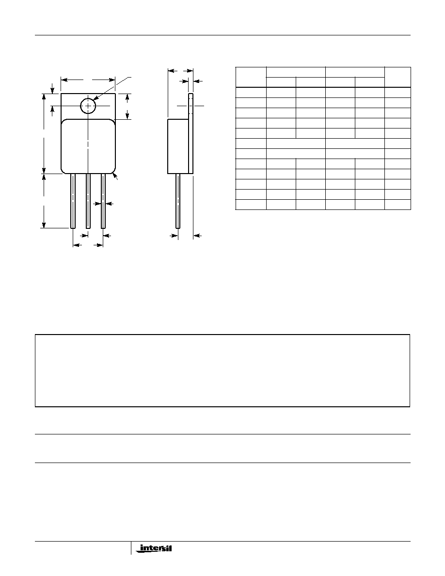
TO-254AA
3 LEAD JEDEC TO-254AA HERMETIC METAL PACKAGE
D
L
Q
H
1
e
e
1
J
1
A
1
A
E
ÿP
ÿ
b
0.065 R MAX.
TYP.
1
2
3
SYMBOL
INCHES
MILLIMETERS
NOTES
MIN
MAX
MIN
MAX
A
0.249
0.260
6.33
6.60
-
A
1
0.040
0.050
1.02
1.27
-
ÿb
0.035
0.045
0.89
1.14
2, 3
D
0.790
0.800
20.07
20.32
-
E
0.535
0.545
13.59
13.84
-
e
0.150 TYP
3.81 TYP
4
e
1
0.300 BSC
7.62 BSC
4
H
1
0.245
0.265
6.23
6.73
-
J
1
0.140
0.160
3.56
4.06
4
L
0.520
0.560
13.21
14.22
-
ÿP
0.139
0.149
3.54
3.78
-
Q
0.110
0.130
2.80
3.30
-
NOTES:
1. These dimensions are within allowable dimensions of Rev. A of
JEDEC outline TO-254AA dated 11-86.
2. Add typically 0.002 inches (0.05mm) for solder coating.
3. Lead dimension (without solder).
4. Position of lead to be measured 0.250 inches (6.35mm) from bottom
of dimension D.
5. Die to base BeO isolated, terminals to case ceramic isolated.
6. Controlling dimension: Inch.
7. Revision 1 dated 1-93.
WARNING!
BERYLLIA WARNING PER MIL-S-19500
Packages containing beryllium oxide (BeO) shall not be ground, machined, sandblasted, or subject to any mechanical operation
which will produce dust containing any beryllium compound. Packages containing any beryllium compound shall not be
subjected to any chemical process (etching, etc.) which will produce fumes containing beryllium or its' compounds.