 | –≠–ª–µ–∫—Ç—Ä–æ–Ω–Ω—ã–π –∫–æ–º–ø–æ–Ω–µ–Ω—Ç: H4244C | –°–∫–∞—á–∞—Ç—å:  PDF PDF  ZIP ZIP |

1
Æ
CAUTION: These devices are sensitive to electrostatic discharge; follow proper IC Handling Procedures.
1-888-INTERSIL or 321-724-7143
|
Intersil (and design) is a registered trademark of Intersil Americas Inc.
Copyright © Intersil Americas Inc. 2002. All Rights Reserved
HA4244
480MHz, 1 x 1 Video Crosspoint
Switch with Synchronous Enable
The HA4244 is a very wide bandwidth 1 x 1 crosspoint switch
ideal for professional video switching, HDTV, computer
monitor routing, and other high performance applications. The
circuit features very low power dissipation, excellent
differential gain and phase, high off isolation, symmetric slew
rates, fast switching, and a latched enable signal. When
disabled, the output is switched to a high impedance state,
making the HA4244 ideal for routing matrix equipment.
The latched enable input allows for synchronized channel
switching. When CLK is low the master control latch loads the
next EN, while the closed slave control latch maintains the
crosspoint in its current state. CLK switching high closes the
master latch, loads the now open slave latch, and enables or
disables the HA4244 according to the current state of the EN
input.
This crosspoint's design ensures that it powers up in the
disabled state to eliminate bus contention concerns, and to
minimize supply current draw at power up.
For applications requiring an asynchronous crosspoint
switch, please refer to the HA4201 and HA4600 data sheets.
Functional Diagram
Timing Diagram
Features
∑ Low Power Dissipation. . . . . . . . . . . . . . . . . . . . . 105mW
∑ Symmetrical Slew Rates . . . . . . . . . . . . . . . . . . 1700V/
µ
s
∑ 0.1dB Gain Flatness. . . . . . . . . . . . . . . . . . . . . . . 250MHz
∑ -3dB Bandwidth . . . . . . . . . . . . . . . . . . . . . . . . . . 480MHz
∑ Off Isolation (100MHz) . . . . . . . . . . . . . . . . . . . . . . . 85dB
∑ Differential Gain and Phase . . . . . . . 0.01%/0.01 Degrees
∑ High ESD Rating . . . . . . . . . . . . . . . . . . . . . . . . . >1800V
∑ TTL Compatible Control Signals
∑ Latched Enable Input for Synchronous Switching
∑ Powers-Up in Disabled State; Avoids Bus Contention
Applications
∑ Professional Video Switching and Routing
∑ Video Multiplexers
∑ Computer Graphics
∑ RF Switching and Routing
∑ PCM Data Routing
Pinout
HA4244
(SOIC)
TOP VIEW
OUT
IN
D
L
Q
C
CLK
EN
D
L
Q
C
CLK
OUT
ENABLED
DIS
DIS
EN
Part Number Information
PART NUMBER
(BRAND)
TEMP.
RANGE (
o
C)
PACKAGE
PKG.
NO.
HA4244CB
(H4244C)
0 to 70
8 Ld SOIC
M8.15
EN
V-
V+
OUT
1
2
3
4
8
7
6
5
GND
IN
NC
CLK
September 1998
File Number 4078.2
OBSO
LETE
PRO
DUCT
No R
ecom
mend
ed Re
place
ment
2
Absolute Maximum Ratings
Thermal Information
Voltage Between V+ and V-. . . . . . . . . . . . . . . . . . . . . . . . . . . . 12V
Input Voltage . . . . . . . . . . . . . . . . . . . . . . . . . . . . . . . . . . . V
SUPPLY
Digital Input Current (Note 2) . . . . . . . . . . . . . . . . . . . . . . . . .
±
25mA
Output Current . . . . . . . . . . . . . . . . . . . . . . . . . . . . . . . . . . . . . 20mA
Operating Conditions
Temperature Range. . . . . . . . . . . . . . . . . . . . . . . . . . . . 0
o
C to 70
o
C
Thermal Resistance (Typical, Note 1)
JA
(
o
C/W)
SOIC Package . . . . . . . . . . . . . . . . . . . . . . . . . . . . .
158
Maximum Junction Temperature (Plastic Package) . . . . . . . 150
o
C
Maximum Storage Temperature Range . . . . . . . . . -65
o
C to 150
o
C
Maximum Lead Temperature (Soldering 10s) . . . . . . . . . . . . 300
o
C
(SOIC - Lead Tips Only)
CAUTION: Stresses above those listed in "Absolute Maximum Ratings" may cause permanent damage to the device. This is a stress only rating and operation of the
device at these or any other conditions above those indicated in the operational sections of this specification is not implied.
NOTES:
1.
JA
is measured with the component mounted on an evaluation PC board in free air.
2. If an input signal is applied before the supplies are powered up, the input current must be limited to this maximum value.
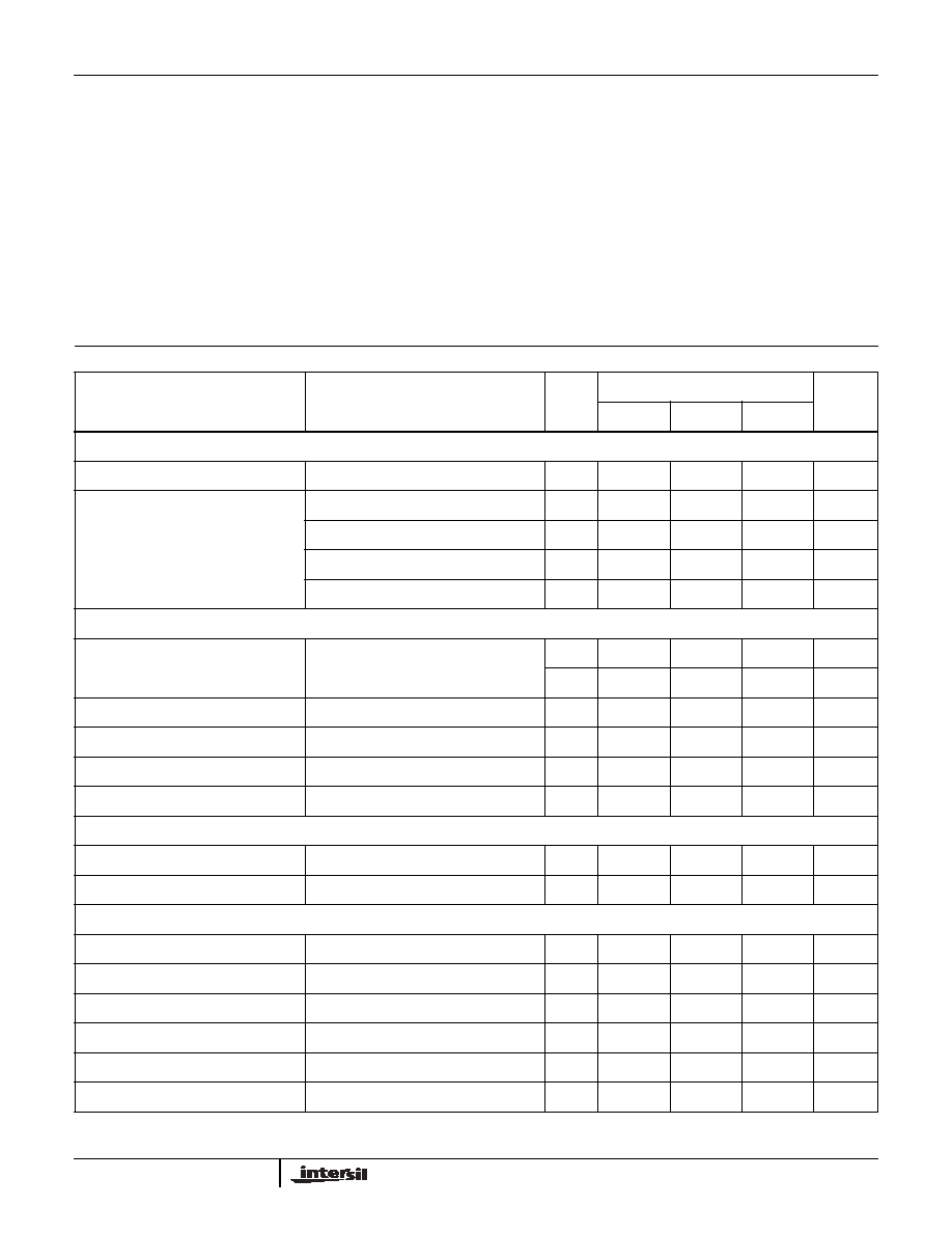
Electrical Specifications
V
SUPPLY
=
±
5V, R
L
= 10k
, V
EN
= 2.0V, Unless Otherwise Specified
PARAMETER
TEST CONDITIONS
TEMP.
(
o
C)
HA4244
UNITS
MIN
TYP
MAX
DC SUPPLY CHARACTERISTICS
Supply Voltage
Full
±
4.5
±
5.0
±
5.5
V
Supply Current
(V
OUT
= 0V)
V
EN
= 2.0V
25, 70
-
10.5
13
mA
V
EN
= 2.0V
0
-
-
14.5
mA
V
EN
= 0.8V
25, 70
-
-
275
µ
A
V
EN
= 0.8V
0
-
-
325
µ
A
ANALOG DC CHARACTERISTICS
Output Voltage Swing without Clipping
V
OUT
= V
IN
±
V
IO
±
20mV
25, 70
±
2.7
±
2.8
-
V
0
±
2.4
±
2.5
-
V
Output Current
Full
15
20
-
mA
Input Bias Current
Full
-
30
50
µ
A
Output Offset Voltage
25
-10
-
10
mV
Output Offset Voltage Drift (Note 3)
Full
-
25
50
µ
V/
o
C
SWITCHING CHARACTERISTICS
Turn-On Time
25
-
160
-
ns
Turn-Off Time
25
-
320
-
ns
DIGITAL DC CHARACTERISTICS
Input Logic High Voltage
Full
2
-
-
V
Input Logic Low Voltage
Full
-
-
0.8
V
EN Input Current
V
EN
= 0 to 4V
Full
-2
-
2
µ
A
CLK Input Current
V
CLK
= 0 to 4V
Full
-10
-
10
µ
A
EN Setup Time to CLK Rising Edge
Full
-
25
-
ns
EN Hold Time after CLKRising Edge
Full
-
10
-
ns
HA4244

3
AC Test Circuit
PC Board Layout
The frequency response of this circuit depends greatly on
the care taken in designing the PC board. The use of low
inductance components such as chip resistors and chip
capacitors is strongly recommended, while a solid
ground plane is a must!
Attention should be given to decoupling the power supplies.
A large value (10
µ
F) tantalum in parallel with a small value
(0.1
µ
F) chip capacitor works well in most cases.
Keep input and output traces as short as possible, because
trace inductance and capacitance can easily become the
performance limiting items.
AC CHARACTERISTICS
Insertion Loss
1V
P-P
Full
-
0.04
0.05
dB
-3dB Bandwidth
R
S
= 82
, C
L
= 10pF
25
-
480
-
MHz
R
S
= 43
, C
L
= 15pF
25
-
380
-
MHz
R
S
= 36
, C
L
= 21pF
25
-
370
-
MHz
±
0.1dB Flat Bandwidth
R
S
= 82
, C
L
= 10pF
25
-
250
-
MHz
R
S
= 43
, C
L
= 15pF
25
-
175
-
MHz
R
S
= 36
, C
L
= 21pF
25
-
170
-
MHz
Input Resistance
Full
200
400
-
k
Input Capacitance
Full
-
1.0
-
pF
Enabled Output Resistance
Full
-
15
-
Disabled Output Capacitance
V
EN
= 0.8V
Full
-
2.0
-
pF
Differential Gain
4.43MHz, Note 3
25
-
0.01
0.02
%
Differential Phase
4.43MHz, Note 3
25
-
0.01
0.02
Degrees
Off Isolation
1V
P-P
, 100MHz, V
EN
= 0.8V, R
L
= 10
Full
-
85
-
dB
Slew Rate
(1.5V
P-P
, +SR/-SR)
R
S
= 82
, C
L
= 10pF
25
-
1750/1770
-
V/
µ
s
R
S
= 43
, C
L
= 15pF
25
-
1460/1360
-
V/
µ
s
R
S
= 36
, C
L
= 21pF
25
-
1410/1360
-
V/
µ
s
Total Harmonic Distortion
Note 3
Full
-
0.01
0.1
%
Disabled Output Resistance
Full
-
12
-
M
NOTE:
3. This parameter is not tested. The limits are guaranteed based on lab characterization, and reflect lot-to-lot variation.
Electrical Specifications
V
SUPPLY
=
±
5V, R
L
= 10k
, V
EN
= 2.0V, Unless Otherwise Specified
(Continued)
PARAMETER
TEST CONDITIONS
TEMP.
(
o
C)
HA4244
UNITS
MIN
TYP
MAX
500
400
510
75
V
OUT
V
IN
75
R
S
HA4244
HFA1100
+
-
C
X
10k
NOTE: C
L
= C
X
+ Test Fixture Capacitance.
HA4244

4
Application Information
General
The HA4244 is a synchronous 1 x 1 crosspoint switch that is
ideal for the matrix element in small, high input-to-output
isolation switchers and routers. The HA4244's low input
capacitance and high input resistance provide excellent
video terminations when used with an external 75
resistor.
This crosspoint contains no feedback or gain setting
resistors, so the output is a true high impedance load when
the IC is disabled (EN = 0).
Synchronizing Latches
The HA4244 contains two latches which gate the EN input,
thereby allowing all the crosspoints in a matrix to switch
states synchronously. The latches also allow the EN input to
be changed without affecting the current state of the
HA4244. Thus, the next channel switch can be set up, and
isn't acted upon until the next rising CLK edge. As long as
the EN signals meet a setup and hold time relative to the
rising CLK edge, all of the HA4244s will assume their new
state at the same time.
Power-Up Disable Function
The double latched EN signal, and single CLK input prevent
the user from controlling the crosspoint state at power-up.
To rectify this situation, the HA4244 incorporates power-up
circuitry to ensure that the crosspoint powers up in the
disabled state. Disabling the HA4244 prevents bus
contention between multiplexed outputs, and minimizes the
switching matrix supply current during power-up. Consider,
for example, a matrix of 625 crosspoints that power-up
randomly. If 50% of them power-up enabled, the required
matrix supply current is 3.3A (313 x 10.5mA), neglecting
output current. If HA4244s are utilized the power-up current
is reduced to 0.125A (625 x 200
µ
A).
Frequency Response
Most applications utilizing the HA4244 require a series
output resistor, R
S
, to tune the response for the specific load
capacitance, C
L
, driven. Bandwidth and slew rate degrade
as C
L
increases (as shown in the Electrical Specification
table), so give careful consideration to component
placement to minimize trace length. As an example, -3dB
bandwidth decreases to 160MHz for C
L
= 100pF, R
S
= 0
.
In big matrix configurations where C
L
is large, better
frequency response is obtained by cascading two levels of
crosspoints in the case of multiplexed outputs, or distributing
the load between two drivers if C
L
is due to bussing and
subsequent stage input capacitance.
Control Signals
EN - The ENABLE input is a TTL/CMOS compatible, active
high input. When driven low this input forces the output to a
true high impedance state and reduces the power
dissipation by two orders of magnitude.
CLK - An active high, TTL/CMOS compatible input that
controls the synchronizing latches. When CLK transistions
low, the current state of the EN input is latched in the IC.
This allows the EN input to be changed to the value
correspending to the next channel switch, without affecting
the HA4244's current state. The HA4244 assumes the new
state on the next rising edge of CLK.
Power Up Considerations
No signals should be applied to the digital inputs before the
power supplies are activated. Latch-up may occur if the
inputs are driven at the time of power up. To prevent latch-
up, the input currents during power up must not exceed the
values listed in the Absolute Maximum Ratings.
Harris' Crosspoint Family
Harris offers a variety of 1 x 1 and 4 x 1 crosspoint switches. In
addition to the HA4244, the 1 x 1 family includes the HA4600,
which is an essentially similar device but without the
synchronizing latches, and the HA4201 asynchronous
crosspoint with a Tally output (enable indicator). The 4 x 1
family is comprised of the HA4314, HA4404, and HA4344. The
HA4314 is a 14 lead basic 4 x 1 crosspoint. The HA4404 is a 16
lead device with Tally outputs to indicate the selected channel.
The HA4344 is a 16 lead crosspoint with synchronized control
lines (A0, A1, CS). With synchronization, the control information
for the next channel switch can be loaded into the crosspoint
without affecting the current state. On a subsequent clock edge
the stored control state effects the desired channel switch.
HA4244

5
Typical Performance Curves
V
SUPPLY
=
±
5V, T
A
= 25
o
C, R
L
= 10k
, Unless Otherwise Specified
FIGURE 1. LARGE SIGNAL PULSE RESPONSE
FIGURE 2. INPUT CAPACITANCE vs FREQUENCY
FIGURE 3. FREQUENCY RESPONSE
FIGURE 4. GAIN FLATNESS
FIGURE 5. OFF ISOLATION
1.0
0.75
0.5
0.25
0
-0.25
-0.5
-0.75
-1.0
O
U
TP
U
T
V
O
LTA
G
E
(V
)
TIME (5ns/DIV.)
1
10
100
FREQUENCY (MHz)
0.75
0.80
0.85
0.90
0.95
1.0
1.05
1.10
1.15
1.20
1.25
500
INP
U
T
CAP
ACIT
ANCE
(
p
F
)
12
9
6
3
0
-3
-6
-9
-12
1
10
100
750
G
A
IN (
d
B)
FREQUENCY (MHz)
R
S
= 36
C
L
= 21pF
R
S
= 43
C
L
= 15pF
R
S
= 82
C
L
= 10pF
0.4
0.3
0.2
0.1
0
-0.1
-0.2
-0.3
-0.4
1
10
100
500
G
A
IN (
d
B)
FREQUENCY (MHz)
R
S
= 36
C
L
= 21pF
R
S
= 82
C
L
= 10pF
R
S
= 43
C
L
= 15pF
-50
-60
-70
-80
-90
-100
-110
-120
-130
1
10
100
500
O
F
F
I
S
O
L
AT
IO
N (
d
B)
FREQUENCY (MHz)
V
IN
= 1V
P-P
R
L
= 10
HA4244
6
Die Characteristics
DIE DIMENSIONS:
51 mils x 36 mils x 19 mils
1290
µ
m x 910
µ
m x 483
µ
m
METALLIZATION:
Type: Metal 1: AlCu (1%)/TiW
Thickness: Metal 1: 6k
≈
±
0.8k
≈
Type: Metal 2: AlCu (1%)
Thickness: Metal 2: 16k
≈
±
1.1k
≈
PASSIVATION:
Type: Nitride
Thickness: 4k
≈
±
0.5k
≈
TRANSISTOR COUNT:
53
SUBSTRATE POTENTIAL (Powered Up):
V-
Metallization Mask Layout
HA4244
EN
V-
V+
OUT
CLK
IN
GND
HA4244