3-161
Features
∑ Programmability
∑ High Rate Slew . . . . . . . . . . . . . . . . . . . . . . . . . . . 30V/
µ
s
∑ Wide Gain Bandwidth . . . . . . . . . . . . . . . . . . . . . 40MHz
∑ High Gain . . . . . . . . . . . . . . . . . . . . . . . . . . . . . . 150kV/V
∑ Low Offset Current . . . . . . . . . . . . . . . . . . . . . . . . . .5nA
∑ High Input Impedance . . . . . . . . . . . . . . . . . . . . . . 30M
∑ Single Capacitor Compensation
∑ DTL/TTL Compatible Inputs
Applications
∑ Thousands of Applications; Program
- Signal Selection/Multiplexing
- Operational Amplifier Gain
- Oscillator Frequency
- Filter Characteristics
- Add-Subtract Functions
- Integrator Characteristics
- Comparator Levels
Description
THA-2400/04/05 comprise a series of four-channel
programmable amplifiers providing a level of versatility
unsurpassed by any other monolithic operational amplifier.
Versatility is achieved by employing four input amplifier
channels, any one (or none) of which may be electronically
selected and connected to a single output stage through
DTL/TTL compatible address inputs. The device formed by
the output and the selected pair of inputs is an op amp which
delivers excellent slew rate, gain bandwidth and power
bandwidth performance. Other advantageous features for
these dielectrically isolated amplifiers include high voltage
gain and input impedance coupled with low input offset
voltage and offset current. External compensation is not
required on this device at closed loop gains greater than 10.
Each channel of the HA-2400/04/05 can be controlled and
operated with suitable feedback networks in any of the
standard op amp configurations. This specialization makes
these amplifiers excellent components for multiplexing signal
selection and mathematical function designs. With 30V/
µ
s
slew rate, 40MHz gain bandwidth and 30M
input
impedance these devices are ideal building blocks for signal
generators, active filters and data acquisition designs.
Programmability, coupled with 4mV typical offset voltage and
5nA offset current, makes these amplifiers outstanding
components for signal conditioning circuits.
During Disable Mode V
OUT
goes to V-. For high output
impedance during Disable, see HA2444.
For further design ideas, see Application Note AN514.
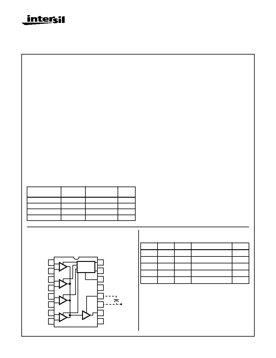
Pinout
HA-2400/04 (CERDIP)
HA-2405 (CERDIP, PDIP)
TOP VIEW)
Ordering Information
PART NUMBER
TEMP.
RANGE (
o
C)
PACKAGE
PKG.
NO.
HA1-2400-2
-55 to 125
16 Ld CERDIP
F16.3
HA1-2404-4
-25 to 85
16 Ld CERDIP
F16.3
HA1-2405-5
0 to 75
16 Ld CERDIP
F16.3
HA3-2405-5
0 to 75
16 Ld PDIP
E16.3
14
15
16
9
13
12
11
10
1
2
3
4
5
7
6
8
3
OUTPUT AMP
ENABLE
D0
D1
GND
COMP
V+
OUT
V-
4
1
2
+IN3
-IN3
+IN4
-IN4
-IN1
+IN1
+IN2
-IN2
3
DECODE
CONTROL
+
-
+
-
+
-
+
-
TRUTH TABLE
D1
D0
EN
SELECTED CHANNEL
D1
L
L
H
1
L
L
H
H
2
L
H
L
H
3
H
H
H
H
4
H
X
X
L
None, V
OUT
goes to V-
X
November 1996
HA-2400, HA-2404,
HA-2405
40MHz, PRAM Four Channel
Programmable Amplifiers
File Number
2891.2
CAUTION: These devices are sensitive to electrostatic discharge; follow proper IC Handling Procedures.
1-888-INTERSIL or 321-724-7143 | Copyright © Intersil Corporation 1999
3-162
Absolute Maximum Ratings
T
A
= 25
o
C
Thermal Information
Voltage Between V+ and V- Terminals . . . . . . . . . . . . . . . . . . 45.0V
Differential Input Voltage. . . . . . . . . . . . . . . . . . . . . . . . . . . V
SUPPLY
Digital Input Voltage . . . . . . . . . . . . . . . . . . . . . . . -0.76V to +10.0V
Output Current . . . . . . . . . . . Short Circuit Protected, I
SC
<
±
33mA)
Internal Power Dissipation (Note 1)
Operating Conditions
Temperature Range
HA-2400-2. . . . . . . . . . . . . . . . . . . . . . . . . . . . . . -55
o
C to 125
o
C
HA-2404-4. . . . . . . . . . . . . . . . . . . . . . . . . . . . . . . -25
o
C to 85
o
C
HA-2405-5. . . . . . . . . . . . . . . . . . . . . . . . . . . . . . . . . 0
o
C to 75
o
C
Thermal Resistance (Typical, Note 2)
JA
(
o
C/W)
JC
(
o
C/W)
PDIP Package . . . . . . . . . . . . . . . . . . .
80
N/A
CERDIP Package . . . . . . . . . . . . . . . .
90
35
Maximum Junction Temperature (Ceramic Package) . . . . . . . . 175
o
C
Maximum Junction Temperature (Plastic Package) . . . . . . . 150
o
C
Maximum Storage Temperature Range . . . . . . . . . -65
o
C to 150
o
C
Maximum Lead Temperature (Soldering 10s) . . . . . . . . . . . . 300
o
C)
CAUTION: Stresses above those listed in "Absolute Maximum Ratings" may cause permanent damage to the device. This is a stress only rating and operation
of the device at these or any other conditions above those indicated in the operational sections of this specification is not implied.
NOTES:
1. Maximum power dissipation including output load, must be designed to maintain the junction temperature below 175
o
C for the ceramic
package, and below 150
o
C for the plastic packages.
2.
JA
is measured with the component mounted on an evaluation PC board in free air.
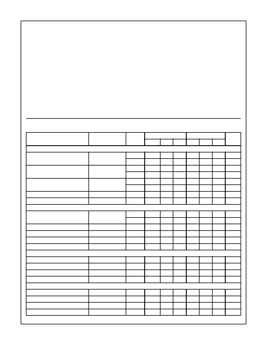
Electrical Specifications
Test Conditions: V
SUPPLY
=
±
15V, Unless Otherwise Specified. Digital Inputs: V
IL
= +0.5V, V
IH
= +2.4.
Limits apply to each of the four channels, when addressed
PARAMETER
TEST
CONDITIONS
TEMP.
(
o
C)
HA-2400/04
HA-2405
UNITS
MIN
TYP
MAX
MIN
TYP
MAX
INPUT CHARACTERISTICS
Offset Voltage
25
-
4
9
-
4
9
mV
Full
-
-
11
-
-
11
mV
Bias Current (Note 8)
25
-
50
200
-
50
250
nA
Full
-
-
400
-
-
500
nA
Offset Current (Note 8)
25
-
5
50
-
5
50
nA
Full
-
-
100
-
-
100
nA
Input Resistance (Note 8)
25
-
30
-
-
30
-
M
Common Mode Range
Full
±
9.0
-
-
±
9.0
-
-
V
TRANSFER CHARACTERISTICS
Large Signal Voltage Gain
R
L
= 2k
25
50
150
-
50
150
-
kV/V
V
OUT
= 20V
P-P
Full
25
-
-
25
-
-
kV/V
Common Mode Rejection Ratio
V
CM
=
±
5V
Full
80
100
-
74
100
-
dB
Gain Bandwidth (Notes 3, 9)
25
20
40
-
20
40
-
MHz
Gain Bandwidth (Notes 4, 9)
25
4
8
-
4
8
-
MHz
Minimum Stable Gain
(C
COMP
= 0)
10
-
-
10
-
-
V/V
OUTPUT CHARACTERISTICS
Output Voltage Swing
R
L
= 2k
Full
±
10.0
±
12.0
-
±
10.0
±
12.0
-
V
Output Current
25
10
20
-
10
20
-
mA
Full Power Bandwidth (Notes 3, 10)
V
OUT
= 20V
P-P
25
640
950
-
640
950
-
kHz
Full Power Bandwidth (Notes 4, 10)
V
OUT
= 20V
P-P
25
200
250
-
200
250
-
kHz
TRANSIENT RESPONSE (Note 11)
Rise Time (Note 4)
V
OUT
= 200mV
PEAK
25
-
20
45
-
20
50
ns
Overshoot (Note 4)
V
OUT
= 200mV
PEAK
25
-
25
40
-
25
40
%
Slew Rate (Note 3)
V
OUT
= 10V
P-P
25
20
30
-
20
30
-
V/
µ
s
Slew Rate (Notes 4, 9)
V
OUT
= 10V
P-P
25
6
8
-
6
8
-
V/
µ
s
HA-2400, HA-2404, HA-2405
3-163
Schematic Diagram
HA-2400
Settling Time (Notes 4, 5, 9)
V
OUT
= 10V
P-P
25
-
1.5
2.5
-
1.5
2.5
µ
s
CHANNEL SELECT CHARACTERISTICS
Digital Input Current
V
IN
= 0V
Full
-
1
1.5
-
1
1.5
mA
Digital Input Current
V
IN
= +5.0V
Full
-
5
-
-
5
-
nA
Output Delay (Notes 6, 9)
25
-
100
250
-
100
250
ns
Crosstalk (Note 7)
25
-80
-110
-
-74
-110
-
dB
POWER SUPPLY CHARACTERISTICS
Supply Current
25
-
4.8
6.0
-
4.8
6.0
mA
Power Supply Rejection Ratio
V
S
=
±
10V to
±
20V
Full
74
90
-
74
90
-
dB
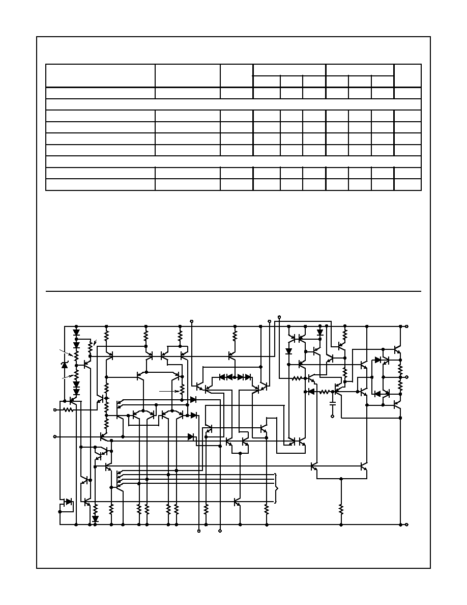
NOTES:
3. A
V
= +10, C
COMP
= 0, R
L
= 2k
, C
L
= 50pF.
4. A
V
= +1, C
COMP
= 15pF, R
L
= 2k
, C
L
= 50pF.
5. To 0.1% of final value.
6. To 10% of final value; output then slews at normal rate to final value.
7. Unselected input to output; V
IN
=
±
10V
DC
.
8. Unselected channels have approximately the same input parameters.
9. Guaranteed by design.
10. Full Power Bandwidth based on slew rate measurement using:
.
11. See Figure 13 for test circuit.
Electrical Specifications
Test Conditions: V
SUPPLY
=
±
15V, Unless Otherwise Specified. Digital Inputs: V
IL
= +0.5V, V
IH
= +2.4.
Limits apply to each of the four channels, when addressed (Continued)
PARAMETER
TEST
CONDITIONS
TEMP.
(
o
C)
HA-2400/04
HA-2405
UNITS
MIN
TYP
MAX
MIN
TYP
MAX
FPBW
SR
2
V
PEAK
---------------------------
V
PEAK
;
5V
=
=
ENABLE
GND
OUT
R
2
2.4K
R
4
22.9K
Q
1
Q
3
Q
4
Q
6
Q
7
Q
8
R
1
1.6K
R
3
1.8K
Q
2
Q
5
R
5
8.0K
R
6
2.0K
R
35
1.6K
R
7
5.6K
Q
10
Q
11
Q
13
Q
12
Q
15
Q
14
R
8
4K
Q
16
R
9
1.5K
R
10
10K
R
11
10K
VA
VC
Q17
VB
Q
18
Q
19
Q
20
VD
R
12
1.6K
Q
28
VE
R
13
0.8K
Q
22
R
15
10K
R
16
10K
Q
21
Q
26
Q
27
R
14
10K
Q
29
Q
23
Q
24
Q
25
Q
30
Q
32
Q
33
Q
102
Q
34
Q
38
R
18
2.0K
Q
103
Q
35
Q
31
Q
36
Q
37
Q
39
Q
40
Q
41
Q
79
Q
81
Q
82
Q
84
Q
80
Q
83
Q
86
Q
89
Q
88
R
35
0.75K
Q
85
Q
98
Q
92
R
30
1.2K
C
1
9.0pF
V+
Q
93
Q
42
R19
1.6K
TO ADDITIONAL
INPUT STAGES
R
29
0.4K
Q
90
Q
91
R
33
4K
Q
97
Q
100
Q
99
Q
95
Q
94
+V
CC
-V
EE
R
31
36.5
R
32
34
Q
96
COMP
IN-
IN+
D1
D0
R
17
1.6K
Q
87
R
34
1.6K
Q
101
Q
9
Diagram Includes: One Input Stage, Decode Control, Bias Network, and Output Stage
HA-2400, HA-2404, HA-2405
3-164
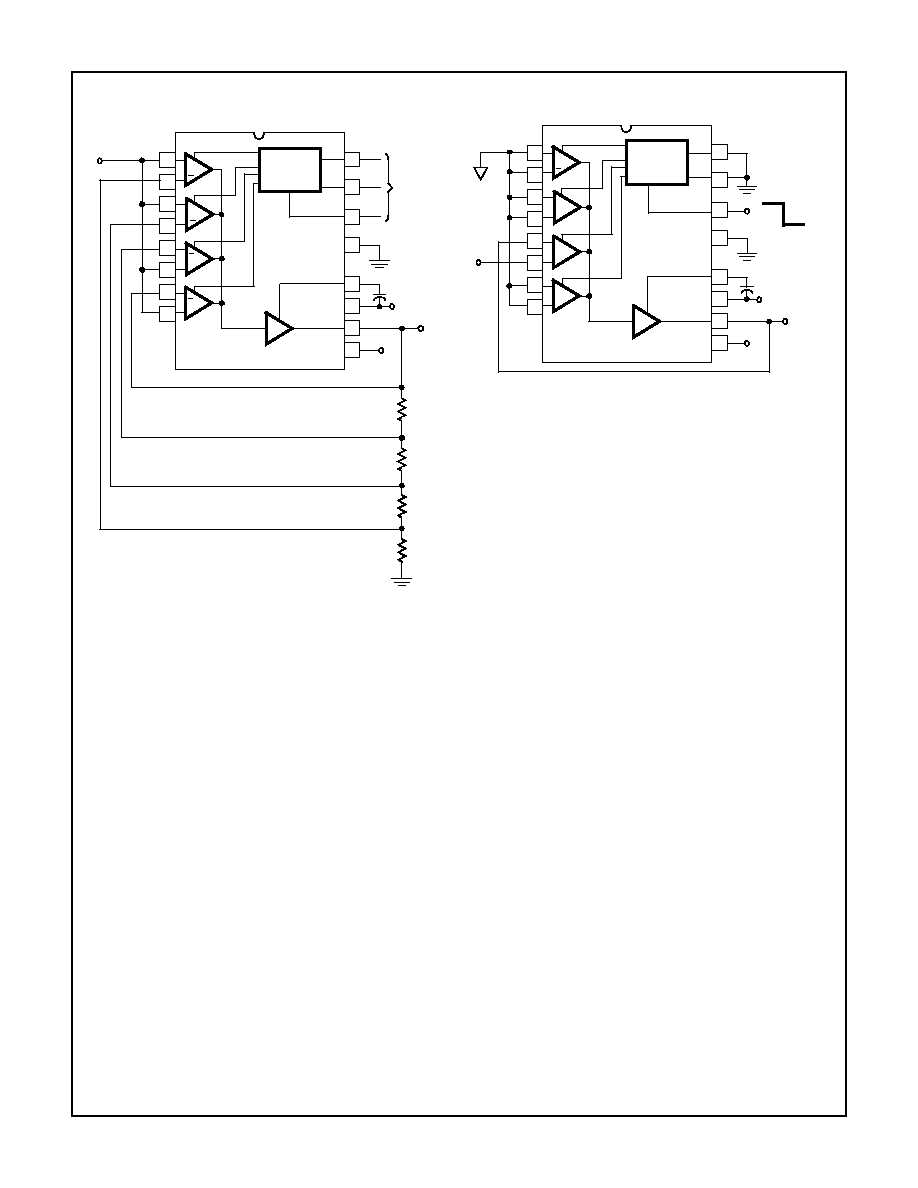
Typical Applications
FIGURE 1. HA-2400 AMPLIFIER, NONINVERTING
PROGRAMMABLE GAIN
FIGURE 2. HA-2400 SAMPLE AND HOLD
For more examples, see Intersil Application Note AN514.
+ 2
1K
500
500
ENABLE
GND
COMP
OUTPUT
AMP
V-
13
8
1
2
3
4
5
7
6
V+
+
4
+
3
+
1
14
15
16
12
11
10
9
+
D1
D0
15pF
IN
2K
-15V
DECODE/
CONTROL
DIGITAL
DIGITAL
GROUND
CONTROL
+15V
OUT
1
ENABLE
GND
COMP
OUTPUT
AMP
V-
13
8
1
2
3
4
5
7
6
V+
+
4
+
3
+
+2
14
15
16
12
11
10
9
D1
D0
-15V
DIGITAL
GROUND
+15V
C
OUT
S
H
IN
DECODE/
CONTROL
I
1
150 x 10
-6
A
I
2
200 x 10
-9
A at 25
o
C
600 x 10
-9
A at -55
o
C
100 x 10
-9
A at 125
o
C
Q
2 x 10
-12
C
Sample Charging Rate
I
1
C
-----
V s
/
=
Hold Drift Rate
I
2
C
-----
V s
/
=
Switch Pedestal Error
Q
C
----
V
=
-
-
-
HA-2400, HA-2404, HA-2405
3-165
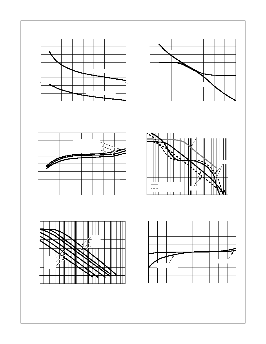
Typical Performance Curves
FIGURE 3. INPUT BIAS CURRENT AND OFFSET CURRENT vs
TEMPERATURE
FIGURE 4. NORMALIZED AC PARAMETERS vs TEMPERATURE
FIGURE 5. POWER SUPPLY CURRENT vs TEMPERATURE
FIGURE 6. OPEN LOOP FREQUENCY AND PHASE RESPONSE
FIGURE 7. FREQUENCY RESPONSE vs C
COMP
FIGURE 8. NORMALIZED AC PARAMETERS vs SUPPLY
VOLTAGE
TEMPERATURE (
o
C)
-55
-50
-25
0
25
50
75
100
125
CURRENT (nA)
0
5
10
40
60
80
100
120
140
BIAS CURRENT
OFFSET CURRENT
TEMPERATURE (
o
C)
-55
-50
-25
0
25
50
75
100
125
NORMALIZED V
ALUE REFERRED T
O
25
o
C
0.8
0.9
1.0
1.1
1.2
BANDWIDTH
SLEW RATE
TEMPERATURE (
o
C)
-55
-50
-25
0
25
50
75
100
125
SUPPL
Y CURRENT (mA)
3
4
5
V
SUPPLY
=
±
20V
V
SUPPLY
=
±
15V
V
SUPPLY
=
±
10V
CROSSTALK REJECTION, A
V
= +1
C
COMP
= 0pF
PHASE
C
COMP
= 15pF
GAIN
OPEN LOOP V
O
L
T
A
GE GAIN (dB)
-20
0
20
40
60
80
100
120
FREQUENCY (Hz)
10
100
1K
10K
100K
1M
10M
100M
0
30
60
90
120
150
180
210
PHASE (DEGREES)
FREQUENCY (Hz)
10
100
1K
10K
100K
1M
10M
100M
OPEN LOOP V
O
L
T
A
GE GAIN (dB)
-20
0
20
40
60
80
100
120
1000pF
300pF
100pF
30pF
15pF
0pF
SLEW RATE
BANDWIDTH
SUPPLY VOLTAGE (V)
±
10
±
20
±
15
0.8
0.9
1.0
1.1
1.2
NORMALIZED V
ALUE REFERRED T
O
±
15V
HA-2400, HA-2404, HA-2405