
5-1
November 1996
HA-2420, HA-2425
3.2
µ
s Sample and Hold Amplifiers
Features
∑ Maximum Acquisition Time
- 10V Step to 0.1%. . . . . . . . . . . . . . . . . . . . . 4
µ
s (Max)
- 10V Step to 0.01%. . . . . . . . . . . . . . . . . . . . 6
µ
s (Max)
∑ Low Droop Rate (C
H
= 1000pF). . . . . . . . 5
µ
V/ms (Typ)
∑ Gain Bandwidth Product . . . . . . . . . . . . . 2.5MHz (Typ)
∑ Low Effective Aperture Delay Time . . . . . . . 30ns (Typ)
∑ TTL Compatible Control Input
∑
±
12V to
±
15V Operation
Applications
∑ 12-Bit Data Acquisition
∑ Digital to Analog Deglitcher
∑ Auto Zero Systems
∑ Peak Detector
∑ Gated Operational Amplifier
Description
The HA-2420 and HA-2425 is a monolithic circuit consisting
of a high performance operational amplifier with its output in
series with an ultra-low leakage analog switch and JFET
input unity gain amplifier.
With an external hold capacitor connected to the switch output,
a versatile, high performance sample-and-hold or track-and-
hold circuit is formed. When the switch is closed, the device
behaves as an operational amplifier, and any of the standard op
amp feedback networks may be connected around the device
to control gain, frequency response, etc. When the switch is
opened the output will remain at its last level.
Performance as a sample-and-hold compares very favorably
with other monolithic, hybrid, modular, and discrete circuits.
Accuracy to better than 0.01% is achievable over the
temperature range. Fast acquisition is coupled with superior
droop characteristics, even at high temperatures. High slew
rate, wide bandwidth, and low acquisition time produce
excellent dynamic characteristics. The ability to operate at
gains greater than 1 frequently eliminates the need for
external scaling amplifiers.
The device may also be used as a versatile operational
amplifier with a gated output for applications such as analog
switches, peak holding circuits, etc. For more information,
please see Application Note AN517.
The MIL-STD-883 data sheet for this device is available on
request.
Pinouts
Ordering Information
PART NUMBER
TEMP.
RANGE (
o
C)
PACKAGE
PKG.
NO.
HA1-2420-2
-55 to 125
14 Ld CERDIP
F14.3
HA1-2425-5
0 to 75
14 Ld CERDIP
F14.3
HA3-2425-5
0 to 75
14 Ld PDIP
E14.3
HA4P2425-5
0 to 75
20 Ld PLCC
N20.35
HA9P2425-5
0 to 75
14 Ld SOIC
M14.15
HA-2420 (CERDIP)
HA-2425 (CERDIP, PDIP, SOIC)
TOP VIEW
HA-2425
(PLCC)
TOP VIEW
-IN
+IN
OFFSET ADJ.
OFFSET ADJ.
V-
NC
OUTPUT
S/H CONTROL
GND
NC
HOLD CAP.
NC
V+
NC
1
2
3
4
5
6
7
14
13
12
11
10
9
8
GND
NC
NC
NC
OFFSET ADJ.
NC
OFFSET ADJ.
NC
NC
OUT
NC
NC
NC
HOLD CAP.
V+
-IN
+IN
V-
S/H
NC
19
3
2
20
1
15
16
17
18
14
9
10 11 12 13
4
5
6
7
8
File Number
2856.2
CAUTION: These devices are sensitive to electrostatic discharge; follow proper IC Handling Procedures.
1-888-INTERSIL or 321-724-7143 | Copyright © Intersil Corporation 1999

5-2
Absolute Maximum Ratings
Thermal Information
Voltage Between V+ and V- Terminals . . . . . . . . . . . . . . . . . . . . 40V
Differential Input Voltage. . . . . . . . . . . . . . . . . . . . . . . . . . . . . . . 24V
Digital Input Voltage (Sample and Hold Pin) . . . . . . . . . . +8V, -15V
Output Current . . . . . . . . . . . . . . . . . . . . . . . Short Circuit Protected
Operating Conditions
Temperature Range
HA-2420-2. . . . . . . . . . . . . . . . . . . . . . . . . . . . . . -55
o
C to 125
o
C
HA-2425-5. . . . . . . . . . . . . . . . . . . . . . . . . . . . . . . . . 0
o
C to 75
o
C
Supply Voltage Range (Typical) . . . . . . . . . . . . . . . . .
±
12V to
±
15V
Thermal Resistance (Typical, Note 1)
JA
(
o
C/W)
JC
(
o
C/W)
CERDIP Package . . . . . . . . . . . . . . . . . .
90
35
PDIP Package . . . . . . . . . . . . . . . . . . . . .
100
N/A
PLCC Package . . . . . . . . . . . . . . . . . . . .
75
N/A
SOIC Package . . . . . . . . . . . . . . . . . . . . .
120
N/A
Maximum Junction Temperature (Ceramic Packages) . . . . . . . 175
o
C
Maximum Junction Temperature (Plastic Package) . . . . . . . . 150
o
C
Maximum Storage Temperature Range . . . . . . . . . -65
o
C to 150
o
C
Maximum Lead Temperature (Soldering 10s) . . . . . . . . . . . . . 300
o
C
(PLCC and SOIC - Lead Tips Only)
CAUTION: Stresses above those listed in "Absolute Maximum Ratings" may cause permanent damage to the device. This is a stress only rating and operation
of the device at these or any other conditions above those indicated in the operational sections of this specification is not implied.
NOTE:
1.
JA
is measured with the component mounted on an evaluation PC board in free air.
Electrical Specifications
Test Conditions (Unless Otherwise Specified) V
SUPPLY
=
±
15.0V; C
H
= 1000pF; Digital Input: V
IL
= +0.8V
(Sample), V
IH
= +2.0V (Hold), Unity Gain Configuration (Output tied to Negative Input)
PARAMETER
TEST
CONDITIONS
TEMP.
(
o
C)
HA-2420-2
HA-2425-5
UNITS
MIN
TYP
MAX
MIN
TYP
MAX
INPUT CHARACTERISTICS
Input Voltage Range
Full
±
10
-
-
±
10
-
-
V
Offset Voltage
25
-
2
4
-
3
6
mV
Full
-
3
6
-
4
8
mV
Bias Current
25
-
40
200
-
40
200
nA
Full
-
-
400
-
-
400
nA
Offset Current
25
-
10
50
-
10
50
nA
Full
-
-
100
-
-
100
nA
Input Resistance
25
5
10
-
5
10
-
M
Common Mode Range
Full
±
10
-
-
±
10
-
-
V
TRANSFER CHARACTERISTICS
Large Signal Voltage Gain
R
L
= 2k
, V
O
= 20V
P-P
Full
25
50
-
25
50
-
kV/V
Common Mode Rejection
V
CM
=
±
10V
Full
80
90
-
74
90
-
dB
Hold Mode Feedthrough Attenuation
(Note 2)
f
IN
100kHz
Full
-
-76
-
-
-76
-
dB
Gain Bandwidth Product (Note 2)
25
-
2.5
-
-
2.5
-
MHz
OUTPUT CHARACTERISTICS
Output Voltage Swing
R
L
= 2k
Full
±
10
-
-
±
10
-
-
V
Output Current
25
±
15
-
-
±
15
-
-
mA
Full Power Bandwidth (Note 2)
V
O
= 20V
P-P
25
-
100
-
-
100
-
kHz
Output Resistance
DC
25
-
0.15
-
-
0.15
-
TRANSIENT RESPONSE
Rise Time (Note 2)
V
O
= 200mV
P-P
25
-
75
100
-
75
100
ns
Overshoot (Note 2)
V
O
= 200mV
P-P
25
-
25
40
-
25
40
%
Slew Rate (Note 2)
V
O
= 10V
P-P
25
3.5
5
-
3.5
5
-
V/
µ
s
DIGITAL INPUT CHARACTERISTICS
Digital Input Current
V
IN
= 0V
Full
-
-
-0.8
-
-
-0.8
mA
V
IN
= 5V
Full
-
-
20
-
-
20
µ
A
Digital Input Voltage
Low
Full
-
-
0.8
-
-
0.8
V
High
Full
2.0
-
-
2.0
-
-
V
SAMPLE AND HOLD CHARACTERISTICS
Acquisition Time (Note 2)
To 0.1% 10V Step
25
-
2.3
4
-
2.3
4
µ
s
HA-2420, HA-2425
5-3
Acquisition Time (Note 2)
To 0.01% 10V Step
25
-
3.2
6
-
3.2
6
µ
s
Hold Step Error
V
IN
= 0V
25
-
10
20
-
10
20
mV
Hold Mode Settling Time
To
±
1mV
25
-
860
-
-
860
-
ns
Aperture Time (Note 3)
25
-
30
-
-
30
-
ns
Effective Aperture Delay Time
25
-
30
-
-
30
-
ns
Aperture Uncertainty
25
-
5
-
-
5
-
ns
Drift Current (Note 2)
V
IN
= 0V
25
-
5
-
-
5
-
pA
HA1-2420
Full
-
1.8
10
-
-
-
nA
HA1-2425
Full
-
-
-
-
0.1
1.0
nA
HA3-2425, HA4P2425, HA9P2425
Full
-
-
-
-
7.5
10.0
nA
POWER SUPPLY CHARACTERISTICS
Supply Current (+)
25
-
3.5
5.5
-
3.5
5.5
mA
Supply Current (-)
25
-
2.5
3.5
-
2.5
3.5
mA
Power Supply Rejection
Full
80
90
-
74
90
-
dB
NOTES:
2. A
V
=
±
1, R
L
= 2k
, C
L
= 50pF.
3. Derived from computer simulation only; not tested.
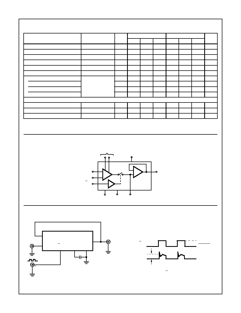
Functional Diagram
Electrical Specifications
Test Conditions (Unless Otherwise Specified) V
SUPPLY
=
±
15.0V; C
H
= 1000pF; Digital Input: V
IL
= +0.8V
(Sample), V
IH
= +2.0V (Hold), Unity Gain Configuration (Output tied to Negative Input) (Continued)
PARAMETER
TEST
CONDITIONS
TEMP.
(
o
C)
HA-2420-2
HA-2425-5
UNITS
MIN
TYP
MAX
MIN
TYP
MAX
4
3
OFFSET
ADJUST
V+
9
13
5
14
2
1
CONTROL
S/H
+INPUT
-INPUT
GND
V-
HA-2420/2425
7
OUT
11
HOLD
CAPACITOR
+
-
+
-
Test Circuits and Waveforms
FIGURE 1. HOLD STEP ERROR AND DRIFT CURRENT
FIGURE 2. HOLD STEP ERROR TEST
-IN
+IN
S/H
CONTROL
OUTPUT
INPUT
S/H CONTROL
INPUT
HOLD
CAP
GND
C
H
S/H
OUTPUT
CONTROL
V
STEP
HOLD
SAMPLE
NOTE: Set rise/fall times of S/H Control to approximately 20ns.
HA-2420, HA-2425

5-4
Schematic Diagram
FIGURE 3. DRIFT CURRENT TEST
FIGURE 4. HOLD MODE FEEDTHROUGH ATTENUATION
Test Circuits and Waveforms
(Continued)
OUTPUT
S/H
CONTROL
HOLD
SAMPLE
V
t
NOTE: Measure the slope of the output during hold,
V/
t,
and compute drift current from: I
D
= C
H
V/
t.
IN2
IN1
IN3
IN4
IN5
IN6
IN7
IN8
A2
A1
A0
EN
OUT
HI-508A
MUX
+5V
SINE WAVE
INPUT
S/H CONTROL INPUT
-IN
+IN
OUT
V
O
S/H
CONTROL
HOLD
CAP GND
C
H
V
INP-P
HA-2420/2425
NOTE: Compute hold mode feedthrough attenuation from the formula:
Where V
OUT
HOLD = Peak-to-Peak value of output
sinewave during the hold mode.
Feedthrough Attenuation
20
V
O UT
HOLD
V
IN
HOLD
----------------------------------
log
=
S/H
CONTROL
GND
R
P
D
1
Q
3
Q
8
Q
7
R
11
Q
12
Q
14
Q
10
Q
13
Q
103
Q
16
Q
105
Q
9
Q
11
Q
82
Q
106
Q
5
Q
17
Q
18
Q
Q
15
Q
2
Q
4
Q
6
Q
21
Q
20
Q
22
Q
23
Q
26
Q
25
Q
24
Q
27
R
1
Q
29
R
2
Q
30
Q
31
Q
35
Q
38
R
13
Q
33
Q
34
Q
32
Q
39
Q
40
Q
41
Q
44
Q
43
Q
42
OFFSET ADJ.
Q
56
Q
100
Q
101
Q
55
Q
83
Q
50
Q
48
Q
45
Q
46
Q
51
Q
59
Q
58
R
7
Q
54
Q
53
Q
52
C
4
J
60
Q
64
Q
65
Q
66
V+
C
H
Q
72
Q
73
Q
74
OUT
R
9
R
8
Q
75
C
3
15pF
Q
77
Q
76
Q
68
Q
78
Q
67
Q
69
R
10
Q
70
Q
79
Q
102
V-
-IN
R
14
Q
80
Q
81
Q
71
Q
62
19
Q
83
Q
91
Q
90
Q
89
Q
87
+IN
Q
47
Q
49
J
61
J
63
J
57
GND
R
121
J
86
HA-2420, HA-2425

5-5
Application Information
Offset Adjustment
The offset voltage of the HA-2420 and HA-2425 may be
adjusted using a 100k
trim pot, as shown in Figure 8. The
recommended adjustment procedure is:
Apply 0V to the sample-and-hold input, and a square wave
to the S/H control.
Adjust the trim pot for 0V output in the hold mode.
Gain Adjustment
The linear variation in pedestal voltage with sample-and- hold
input voltage causes a -0.06% gain error (C
H
= 1000pF). In
some applications (D/A deglitcher, A/D converter) the gain
error can be adjusted elsewhere in the system, while in other
applications it must be adjusted at the sample-and-hold. The
two circuits shown below demonstrate how to adjust gain error
at the sample-and-hold.
The recommended procedure for adjusting gain error is:
1. Perform offset adjustment.
2. Apply the nominal input voltage that should produce a
+10V output.
3. Adjust the trim pot for +10V output in the hold mode.
4. Apply the nominal input voltage that should produce a
-10V output.
5. Measure the output hold voltage (V
-10NOMINAL
). Adjust
the trim pot for an output hold voltage of
Figure 8 shows a typical unity gain circuit, with Offset Zero-
ing. All of the other normal op amp feedback configurations
may be used with the HA-2420/2425. The input amplifier
may be used as a gated amplifier by utilizing Pin 11 as the
output. This amplifier has excellent drive capabilities along
with exceptionally low switch leakage.
The method used to reduce leakage paths on the PC board
and the device package is shown in Figure 9. This guard ring
is recommended to minimize the drift during hold mode.
The hold capacitor should have extremely high insulation
resistance and low dielectric absorption. Polystyrene (below
85
o
C), Teflon, or Parlene types are recommended.
For more applications, consult Intersil Application Note
AN517, or the factory applications group.
0
+10
5
-5
-10
-15
-20
-25
-30
-35
-10
-5
+5
+10
DC INPUT VOLTAGE (V)
HOLD STEP VOLTAGE (mV)
C
H
= 100pF
C
H
= 1000pF
C
H
= 10,000pF
C
H
= 0.1
µ
F
FIGURE 5. HOLD STEP vs INPUT VOLTAGE
V
10
≠
NOMINAL
(
)
-10V
(
)
+
2
----------------------------------------------------------------------------
-IN
+IN
OUT
S/H
CONTROL
OUTPUT
R
I
R
F
0.002R
F
INPUT
S/H CONTROL INPUT
NOTE: GAIN
R
F
≠
R
I
-----------
FIGURE 6. INVERTING CONFIGURATION
+IN
-IN
OUT
S/H
CONTROL
OUTPUT
INPUT
S/H CONTROL
INPUT
NOTE: GAIN ~ 1
R
F
R
I
--------
+
R
F
R
I
0.002R
I
FIGURE 7. NON-INVERTING CONFIGURATION
IN
V-
100k
OFFSET TRIM (
±
25mV RANGE)
OUT
V+
CONTROL
C
H
-
+
-
+
FIGURE 8. BASIC SAMPLE-AND-HOLD (TOP VIEW)
-IN
+IN
V-
V+
GND
CONTROL
OUT
HOLD
CAPACITOR
FIGURE 9. GUARD RING LAYOUT (BOTTOM VIEW)
HA-2420, HA-2425

5-6
Glossary of Terms
Acquisition Time
The time required following a "sample" command, for the output
to reach its final value within
±
0.1% or
±
0.01%. This is the mini-
mum sample time required to obtain a given accuracy, and
includes switch delay time, slewing time and settling time.
Aperture Time
The time required for the sample-and-hold switch to open,
independent of delays through the switch driver and input
amplifier circuitry. The switch opening time is that interval
between the conditions of 10% open and 90% open.
Effective Aperture Delay Time (EADT)
The difference between the digital delay time from the Hold
command to the opening of the S/H switch, and the propaga-
tion time from the analog input to the switch.
EADT may be positive, negative or zero. If zero, the S/H ampli-
fier will output a voltage equal to V
IN
at the instant the Hold
command was received. For negative EADT, the output in Hold
(exclusive of pedestal and droop errors) will correspond to a
value of V
IN
that occurred before the Hold command.
Aperture Uncertainty
The range of variation in Effective Aperture Delay Time. Aper-
ture Uncertainty (also called Aperture Delay Uncertainty,
Aperture Time Jitter, etc.) sets a limit on the accuracy with
which a waveform can be reconstructed from sample data.
Drift Current
The net leakage current from the hold capacitor during the
hold mode. Drift current can be calculated from the droop
rate using the formula:
I
D
(pA)
C
H
(pF)
V
t
--------
◊
(V s
)
/
=
Typical Performance Curves
FIGURE 10. TYPICAL SAMPLE AND HOLD PERFORMANCE AS
A FUNCTION OF HOLDING CAPACITOR
FIGURE 11. BROADBAND NOISE CHARACTERISTICS
FIGURE 12. DRIFT CURRENT vs TEMPERATURE
FIGURE 13. OPEN LOOP FREQUENCY RESPONSE
C
H
VALUE
10pF
100pF
1000pF
0.01
µ
F
0.1
µ
F
1.0
µ
F
1000
100
10
1.0
0.1
0.01
DRIFT DURING HOLD
AT 25
o
C (mV/s)
SLEW RATE
(V/
µ
s)
HOLD STEP
OFFSET
ERROR (mV)
UNITY GAIN
BANDWIDTH
(MHz)
UNITY GAIN PHASE
MARGIN (DEGREES)
MIN. SAMPLE TIME
FOR 0.1% ACCURACY
10V SWINGS (
µ
s)
1000
100
10
1
NOISE (
µ
V
RMS
)
10
100
1K
10K
100K
1M
BANDWIDTH (LOWER 3dB FREQUENCY = 10Hz)
OUTPUT NOISE
"HOLD" MODE
EQUIV. INPUT NOISE
"SAMPLE" MODE - 0
SOURCE RESISTANCE
EQUIV. INPUT NOISE
"SAMPLE" MODE - 100k
SOURCE RESISTANCE
1000
100
10
1
I
D
(pA)
-50
-25
0
25
50
75
100
125
TEMPERATURE (
o
C)
100
90
80
70
60
50
40
30
20
10
0
-10
-20
-30
10
100
1K
10K
100K
1M
10M
100M
FREQUENCY (Hz)
OPEN LOOP V
O
L
T
A
GE GAIN (dB)
C
H
= 100pF
C
H
= 1000pF
C
H
= 0.01
µ
F
C
H
= 1.0
µ
F
C
H
= 0.1
µ
F
HA-2420, HA-2425
5-7
FIGURE 14. HOLD MODE FEED THROUGH ATTENUATION
FIGURE 15. OPEN LOOP PHASE RESPONSE
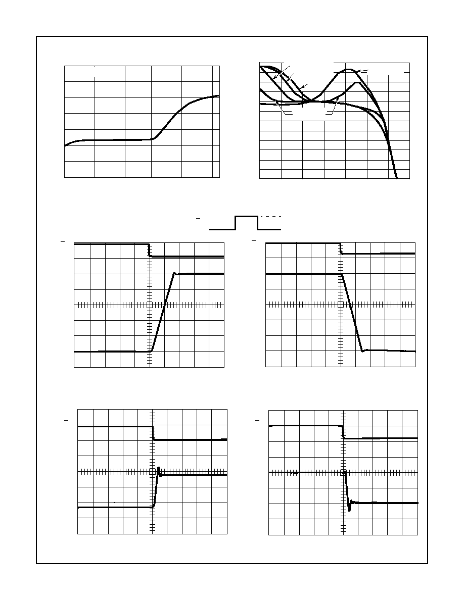
FIGURE 16. ACQUISITION TIME (C
H
= 1000pF)
FIGURE 17. ACQUISITION TIME (C
H
= 1000pF)
FIGURE 18. ACQUISITION TIME (C
H
= 1000pF)
FIGURE 19. ACQUISITION TIME (C
H
= 1000pF)
Typical Performance Curves
(Continued)
-30
-40
-50
-60
-70
-80
-90
100
1K
10K
100K
1M
10M
±
10V SINUSOIDAL INPUT FREQUENCY (Hz)
A
TTENU
A
TION (dB)
C
H
= 1000pF
0
20
40
60
80
100
120
140
160
180
200
220
240
OPEN LOOP PHASE ANGLE (DEGREES)
10
100
1K
10K
100K
1M
10M
100M
FREQUENCY (Hz)
C
H
= 0.01
µ
F
C
H
= 1000pF
C
H
100pF
C
H
= 0.1
µ
F
C
H
= 1.0
µ
F
S/H
CONTROL
SAMPLE
HOLD
4V
0V
S/H
0V
-10V
(2V/DIV.)
V
OUT
(5V/DIV.)
TIME (1
µ
s/DIV.)
0V
S/H
+10V
(2V/DIV.)
V
OUT
(5V/DIV.)
TIME (1
µ
s/DIV.)
0V
TIME (1
µ
s/DIV.)
S/H
-1V
(0.5V/DIV.)
V
OUT
(5V/DIV.)
0V
+1V
TIME (1
µ
s/DIV.)
S/H
(0.5V/DIV.)
V
OUT
(5V/DIV.)
HA-2420, HA-2425

5-8
FIGURE 20. ACQUISITION TIME (C
H
= 1000pF)
FIGURE 21. ACQUISITION TIME (C
H
= 1000pF)
Typical Performance Curves
(Continued)
0V
TIME (500ns/DIV.)
S/H
-0.1V
(50mV/DIV.)
V
OUT
(5V/DIV.)
0V
TIME (500ns/DIV.)
S/H
0.1V
(50mV/DIV.)
V
OUT
(5V/DIV.)
HA-2420, HA-2425
5-9
All Intersil semiconductor products are manufactured, assembled and tested under ISO9000 quality systems certification.
Intersil products are sold by description only. Intersil Corporation reserves the right to make changes in circuit design and/or specifications at any time without
notice. Accordingly, the reader is cautioned to verify that data sheets are current before placing orders. Information furnished by Intersil is believed to be accurate
and reliable. However, no responsibility is assumed by Intersil or its subsidiaries for its use; nor for any infringements of patents or other rights of third parties which
may result from its use. No license is granted by implication or otherwise under any patent or patent rights of Intersil or its subsidiaries.
For information regarding Intersil Corporation and its products, see web site http://www.intersil.com
Die Characteristics
DIE DIMENSIONS:
102 mils x 61 mils x 19 mils
2590
µ
m x 1550
µ
m x 483
µ
m
METALLIZATION:
Type: Al, 1% Cu
Thickness: 16k
≈
±
2k
≈
SUBSTRATE POTENTIAL:
V-
BACKSIDE FINISH:
Gold, Nickel, Silicon, etc.
PASSIVATION:
Type: Nitride (Si
3
N
4
) over Silox (SiO
2
, 5% Phos.)
Silox Thickness: 12k
≈
±
2k
≈
Nitride Thickness: 3.5k
≈
±
1.5k
≈
TRANSISTOR COUNT:
78
PROCESS:
Bipolar Dielectric Isolation
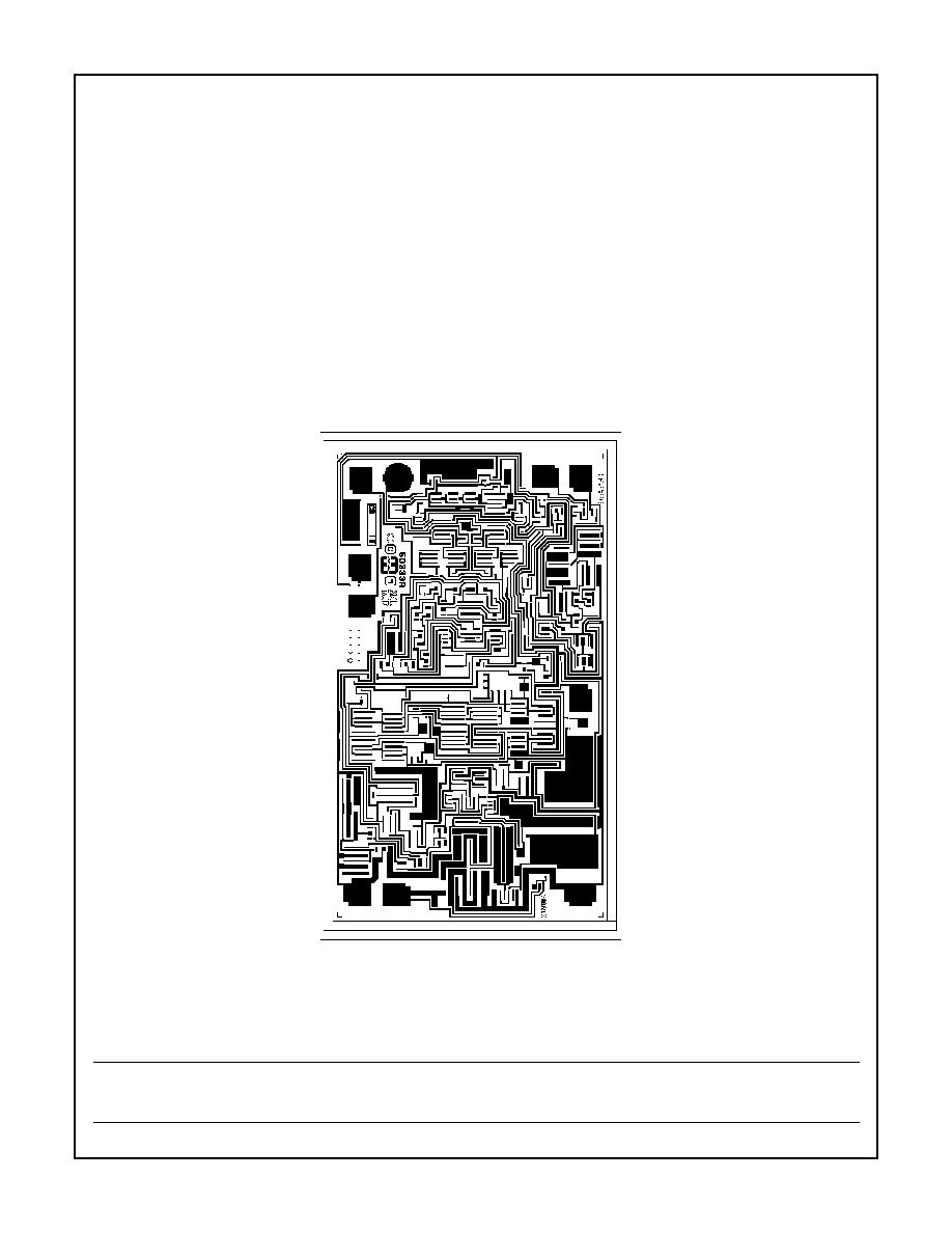
Metallization Mask Layout
HA-2420, HA-2425
GND
HOLD CAP
V+
V-
VOS ADJ
VOS ADJ
OUTPUT
HA-2420, HA-2425