8-3
CAUTION: These devices are sensitive to electrostatic discharge; follow proper IC Handling Procedures.
http://www.intersil.com or 407-727-9207
|
Copyright
©
Intersil Corporation 1999
HA2546/883
Wideband Two Quadrant Analog
Multiplier (Voltage Output)
Description
The HA-2546/883 is a monolithic, high speed, two quadrant,
analog multiplier constructed in the Intersil Dielectrically Iso-
lated High Frequency Process. The HA-2546/883 has a volt-
age output with a 30MHz signal bandwidth, 300V/
µ
s slew
rate and a 17MHz control input bandwidth. High bandwidth
and slew rate make this part an ideal component for use in
video systems. The suitability for precision video applica-
tions is demonstrated further by the 0.1dB gain flatness at
5MHz, 1.6% multiplication error, -52dB feedthrough and dif-
ferential inputs with 1.2
µ
A bias currents. The HA-2546/883
also has low differential gain (0.1% typ.) and phase (0.1
o
typ.) errors.
The HA-2546/883 is well suited for AGC circuits as well as
mixer applications for sonar, radar, and medical imaging
equipment. The voltage output of the HA-2546/883 simplifies
many designs by eliminating the current-to-voltage conver-
sion stage required for current output multipliers.
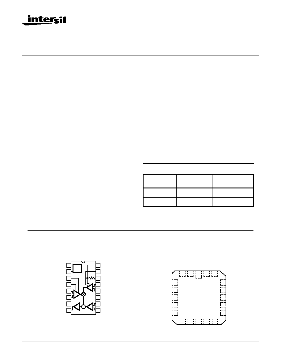
Ordering Information
PART NUMBER
TEMPERATURE
RANGE
PACKAGE
HA1-2546/883
-55
o
C to +125
o
C
16 Lead CerDIP
HA4-2546/883
-55
o
C to +125
o
C
20 Lead Ceramic LCC
Features
∑ This Circuit is Processed in Accordance to MIL-STD-
883 and is Fully Conformant Under the Provisions of
Paragraph 1.2.1.
∑ High Speed Voltage Output. . . . . . . . . . . 300V/
µ
s (Min)
∑ Low Multiplication Error . . . . . . . . . . . . . . . .3.0% (Max)
1.6% (Typ)
∑ Input Bias Currents . . . . . . . . . . . . . . . . . . . . 5
µ
A (Max)
1.2
µ
A (Typ)
∑ Signal Input Feedthrough . . . . . . . . . . . . . . -52dB (Typ)
∑ Wide Signal Bandwidth . . . . . . . . . . . . . . . 30MHz (Typ)
∑ Wide Control Bandwidth . . . . . . . . . . . . . . 17MHz (Typ)
∑ Gain Flatness to 5MHz. . . . . . . . . . . . . . . . 0.10dB (Typ)
Applications
∑ Military Avionics
∑ Missile Guidance Systems
∑ Medical Imaging Displays
∑ Video Mixers
∑ Sonar AGC Processors
∑ Radar Signal Conditioning
∑ Voltage Controlled Amplifier
∑ Vector Generator
July 1994
Pinouts
HA-2546/883
(CERDIP)
TOP VIEW
HA-2546/883
(CLCC)
TOP VIEW
14
15
16
9
13
12
11
10
1
2
3
4
5
7
6
8
GND
V
REF
V
YIO
B
V
YIO
A
V
Y
+
V
Y
-
V
OUT
V-
GA A
GA B
V
X
+
V
X
-
V+
V
Z
-
V
Z
+
GA C
+
-
REF
Y
X
Z
-
+
-
+
-
+
V
YIO
B
V
YIO
A
NC
V
Y
+
V
Y
-
V
REF
GND
NC
GA A
GA C
V-
V
OUT
NC
V
Z
+
V
Z
-
GA B
V
X
+
NC
V
X
-
V+
4
5
6
7
8
10
11
12
13
9
3
2
1
20
19
16
17
18
15
14
Spec Number
511050-883
File Number
2444.1
8-4
Specifications HA2546/883
Absolute Maximum Ratings
Thermal Information
Voltage Between V+ and V- . . . . . . . . . . . . . . . . . . . . . . . . . . . . 35V
Differential Input Voltage . . . . . . . . . . . . . . . . . . . . . . . . . . . . . . . 6V
Output Current . . . . . . . . . . . . . . . . . . . . . . . . . . . . . . . . . . . . . 60mA
Junction Temperature . . . . . . . . . . . . . . . . . . . . . . . . . . . . . . +175
o
C
Storage Temperature Range . . . . . . . . . . . . . . -65
o
C
T
A
+150
o
C
ESD Rating. . . . . . . . . . . . . . . . . . . . . . . . . . . . . . . . . . . . . . <2000V
Lead Temperature (Soldering 10s) . . . . . . . . . . . . . . . . . . . . +300
o
C
Thermal Resistance
JA
JC
CerDIP Package . . . . . . . . . . . . . . . . . . . . . 80
o
C/W
25
o
C/W
Ceramic LCC . . . . . . . . . . . . . . . . . . . . . . . . 61
o
C/W
12
o
C/W
Maximum Package Power Dissipation
CerDIP Package at +75
o
C. . . . . . . . . . . . . . . . . . . . . . . . . . 1.25W
Ceramic LCC Package at +75
o
C. . . . . . . . . . . . . . . . . . . . . 1.64W
Package Power Dissipation Derating Factor above +75
o
C
CerDIP Package . . . . . . . . . . . . . . . . . . . . . . . . . . . . . . 12mW/
o
C
Ceramic LCC Package . . . . . . . . . . . . . . . . . . . . . . . . . 16mW/
o
C
CAUTION: Stresses above those listed in "Absolute Maximum Ratings" may cause permanent damage to the device. This is a stress only rating and operation
of the device at these or any other conditions above those indicated in the operational sections of this specification is not implied.
Operating Conditions
Operating Temperature Range . . . . . . . . . . . . . . . . -55
o
C to +125
o
C
Operating Supply Voltage
. . . . . . . . . . . . . . . . . . . . . . . . . . ±
8V to
±
15V
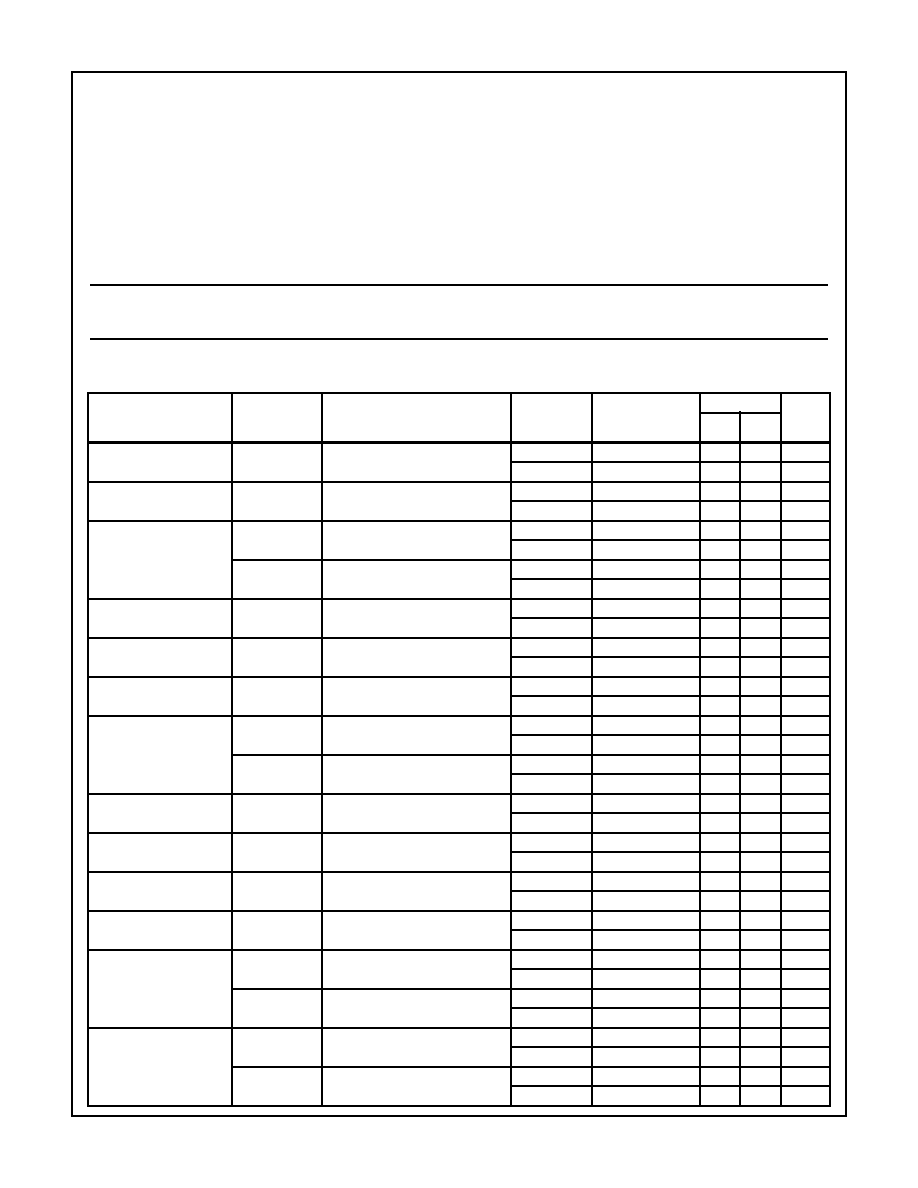
TABLE 1. DC ELECTRICAL PERFORMANCE CHARACTERISTICS
Device Tested at: V
SUPPLY
=
±
15V, R
LOAD
= 1k
, C
LOAD
= 50pF, Unless Otherwise Specified.
PARAMETERS
SYMBOL
CONDITIONS
GROUP A
SUBGROU
PS
TEMPERATURE
LIMITS
UNITS
MIN
MAX
Multiplication Error
ME
V
Y
=
±
5V
1
+25
o
C
-3
3
%FS
2, 3
+125
o
C, -55
o
C
-5
5
%FS
Scale Factor Error
SF
1
+25
o
C
-5
5
%
2, 3
+125
o
C, -55
o
C
-5
5
%
Common Mode Range
+CMR
1
+25
o
C
5
-
V
2, 3
+125
o
C, -55
o
C
5
-
V
-CMR
1
+25
o
C
-
-5
V
2, 3
+125
o
C, -55
o
C
-
-5
V
Input Offset Voltage (V
Y
)
V
IO
(V
Y
)
V
CM
= 0V
1
+25
o
C
-10
10
mV
2, 3
+125
o
C, -55
o
C
-15
15
mV
Input Bias Current (V
Y
)
I
B
(V
Y
)
V
CM
= 0V
1
+25
o
C
-15
15
µ
A
2, 3
+125
o
C, -55
o
C
-20
20
µ
A
Input Offset Current (V
Y
)
I
IO
(V
Y
)
V
CM
= 0V
1
+25
o
C
-2
2
µ
A
2, 3
+125
o
C, -55
o
C
-3
3
µ
A
Common Mode (V
Y
)
Rejection Ratio
+CMRR(V
Y
)
V
Y
= 0 to +5V, V
X
= +2V
1
+25
o
C
60
-
dB
2, 3
+125
o
C, -55
o
C
60
-
dB
-CMRR(V
Y
)
V
Y
= 0 to -5V, V
X
= +2V
1
+25
o
C
60
-
dB
2, 3
+125
o
C, -55
o
C
60
-
dB
Input Offset Voltage (V
X
)
V
IO
(V
X
)
V
CM
= 0V
1
+25
o
C
-2
2
mV
2, 3
+125
o
C, -55
o
C
-15
15
mV
Input Bias Current (V
X
)
I
B
(V
X
)
V
CM
= 0V
1
+25
o
C
-2
2
µ
A
2, 3
+125
o
C, -55
o
C
-5
5
µ
A
Input Offset Current (V
X
)
I
IO
(V
X
)
V
CM
= 0V
1
+25
o
C
-2
2
µ
A
2, 3
+125
o
C, -55
o
C
-3
3
µ
A
Input Offset Voltage (V
Z
)
V
IO
(V
Z
)
V
X
= 0V, V
Y
= 0V
1
+25
o
C
-15
15
mV
2, 3
+125
o
C, -55
o
C
-15
15
mV
Output Voltage Swing
+V
OUT
V
Y
= +5V, V
X
= +2.5V
1
+25
o
C
5
-
V
2, 3
+125
o
C, -55
o
C
5
-
V
-V
OUT
V
Y
= -5V, V
X
= +2.5V
1
+25
o
C
-
-5
V
2, 3
+125
o
C, -55
o
C
-
-5
V
Output Current
+I
OUT
V
Y
= +5V, V
X
= +2.5V
1
+25
o
C
20
-
mA
2, 3
+125
o
C, -55
o
C
20
-
mA
-I
OUT
V
Y
= -5V, V
X
= +2.5V
1
+25
o
C
-
-20
mA
2, 3
+125
o
C, -55
o
C
-
-20
mA
Spec Number
511050-883
8-5
Specifications HA2546/883
Power Supply Rejection
Ratio
+PSRR
V
S
= 3V, V+ = +15V, V- = -15V,
V+ = +12V, V- = -15V
1
+25
o
C
58
-
dB
2, 3
+125
o
C, -55
o
C
58
-
dB
-PSRR
V
S
= 3V, V+ = +15V, V- = -15V,
V+ = +15V, V- = -12V
1
+25
o
C
58
-
dB
2, 3
+125
o
C, -55
o
C
58
-
dB
Quiescent Power Supply
Current
+I
CC
V
X
= V
Y
= 0V, I
OUT
= 0mA
1
+25
o
C
29
-
mA
2, 3
+125
o
C, -55
o
C
29
-
mA
-I
CC
V
X
= V
Y
= 0V, I
OUT
= 0mA
1
+25
o
C
-
-29
mA
2, 3
+125
o
C, -55
o
C
-
-29
mA
TABLE 2. AC ELECTRICAL PERFORMANCE CHARACTERISTICS
Table 2 Intentionally Left Blank. See AC Specifications in Table 3.
TABLE 3. ELECTRICAL PERFORMANCE CHARACTERISTICS
Device Tested at: V
SUPPLY
=
±
15V, R
LOAD
= 1k
, C
LOAD
= 50pF, Unless Otherwise Specified.
PARAMETER
SYMBOL
CONDITIONS
NOTES
TEMPERATURE
LIMITS
UNITS
MIN
MAX
Slew Rate
+SR
V
OUT
= -5V to +5V, V
X
= 2V
DC
1
+25
o
C
300
-
V/
µ
s
1
+125
o
C, -55
o
C
300
-
V/
µ
s
-SR
V
OUT
= +5V to -5V, V
X
= 2V
DC
1
+25
o
C
300
-
V/
µ
s
1
+125
o
C, -55
o
C
300
-
V/
µ
s
Rise and Fall Time
TR
V
OUT
= -100mV to +100mV
V
X
= 2V
DC
1, 3
+25
o
C
-
15
ns
1, 3
+125
o
C, -55
o
C
-
17
ns
TF
V
OUT
= +100mV to -100mV
V
X
= 2V
DC
1, 3
+25
o
C
-
15
ns
1, 3
+125
o
C, -55
o
C
-
17
ns
Overshoot
+OS
V
OUT
= -100mV to +100mV
V
X
= 2V
DC
1
+25
o
C
-
30
%
1
+125
o
C, -55
o
C
-
30
%
-OS
V
OUT
= +100mV to -100mV
V
X
= 2V
DC
1
+25
o
C
-
30
%
1
+125
o
C, -55
o
C
-
30
%
Full Power Bandwidth
FPBW
V
PEAK
= 5V, V
X
= 2V
DC
1, 2
+25
o
C
9.5
-
MHz
1, 2
+125
o
C, -55
o
C
9.5
-
MHz
NOTES:
1. Parameters listed in Table 3 are controlled via design or process parameters and are not directly tested at final production. These param-
eters are lab characterized upon initial design release, or upon design changes. These parameters are guaranteed by characterization
based upon data from multiple production runs which reflect lot to lot and within lot variation.
2. Full Power Bandwidth guarantee based on Slew Rate measurement using FPBW = Slew Rate/(2
V
PEAK
).
3. Measured between 10% and 90% points.
TABLE 4. ELECTRICAL TEST REQUIREMENTS
MIL-STD-883 TEST REQUIREMENTS
SUBGROUPS (SEE TABLE 1)
Interim Electrical Parameters (Pre Burn-in)
1
Final Electrical Test Parameters
1(Note 1), 2, 3
Group A Test Requirements
1, 2, 3
Groups C and D Endpoints
1
NOTE:
1. PDA applies to Subgroup 1 only.
TABLE 1. DC ELECTRICAL PERFORMANCE CHARACTERISTICS
(Continued)
Device Tested at: V
SUPPLY
=
±
15V, R
LOAD
= 1k
, C
LOAD
= 50pF, Unless Otherwise Specified.
PARAMETERS
SYMBOL
CONDITIONS
GROUP A
SUBGROU
PS
TEMPERATURE
LIMITS
UNITS
MIN
MAX
Spec Number
511050-883
8-6
HA2546/883
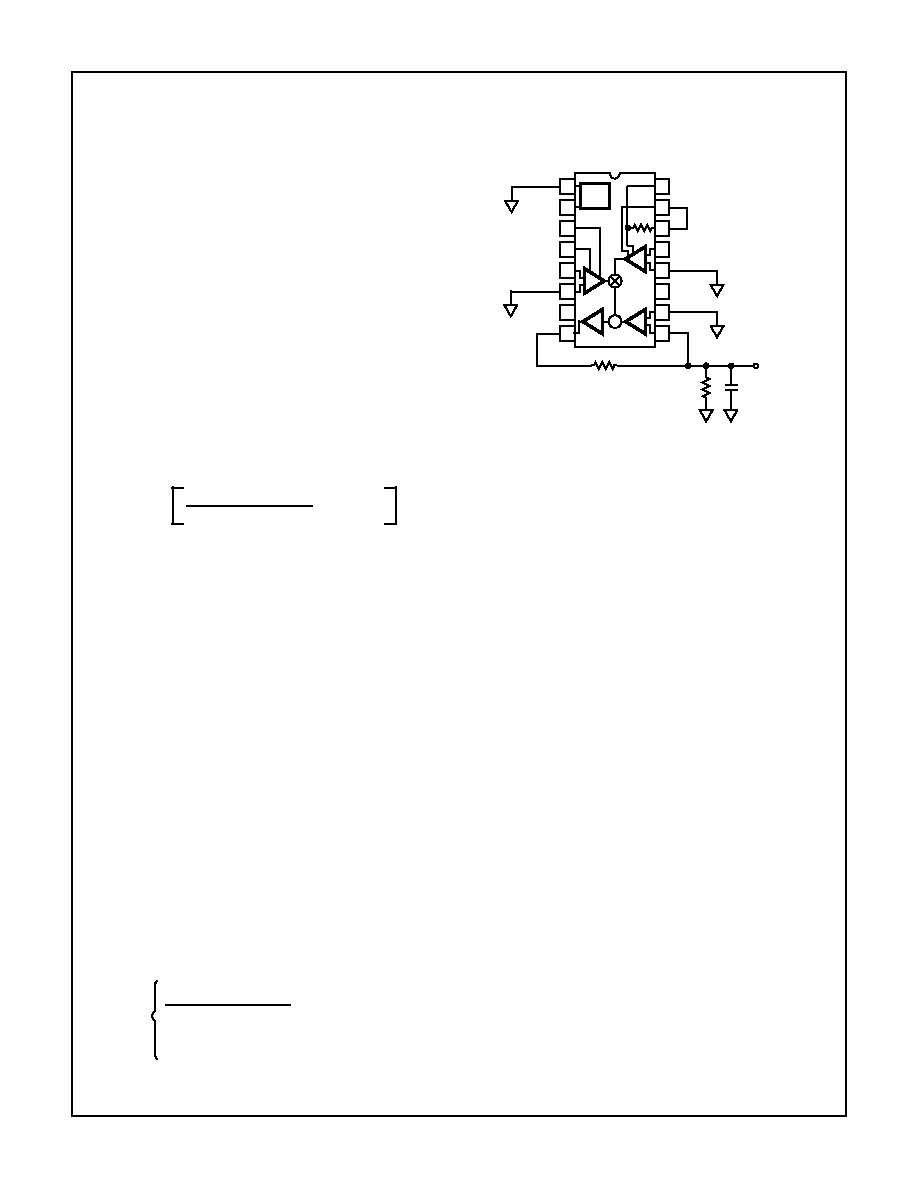
Die Characteristics
DIE DIMENSIONS:
79.9mils x 119.7mils x 19mils
±
1mils
METALLIZATION:
Type: Al, 1%Cu
Thickness: 16k
≈
±
2k
≈
GLASSIVATION:
Type: Nitride (Si
3
N
4
) over Silox (SiO
2
, 5% Phos)
Silox Thickness: 12k
≈
±
1.5k
≈
Nitride Thickness: 3.5k
≈
±
1.5k
≈
WORST CASE CURRENT DENSITY:
0.72 x 10
5
A/cm
2
TRANSISTOR COUNT: 87
Metallization Mask Layout
HA-2546/883
(2)
(1)
V
YIO
B
(3)
V
YIO
A
(4)
V
Y
+
(5)
V
Y
-
(6)
(7)
(8)
(9)
(10)
(11)
V+
(12)
V
X
-
(13)
V
X
+
(14)
GA B
(15)
(16)
GND
V
REF
V-
V
OUT
V
Z
+
V
Z
-
GA A
GA C
Spec Number
511050-883
8-7
Specifications HA2546/883
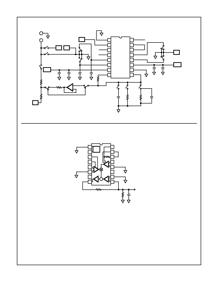
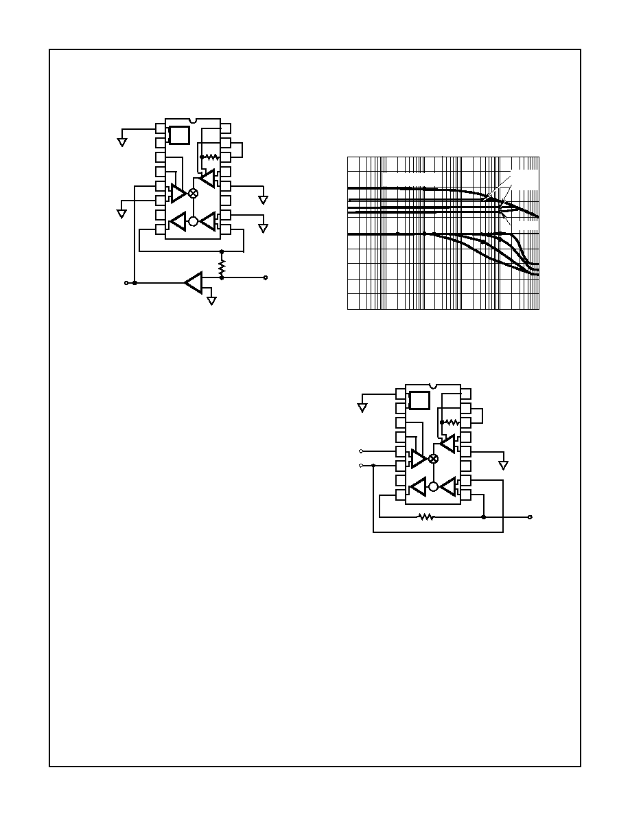
Test Circuit
For Detailed Information, Refer to HA-2546/883 Test Tech Brief
Test Waveforms
LARGE AND SMALL SIGNAL RESPONSE TEST CIRCUIT
GND
V
REF
V
ADJB
V
ADJA
V
Y+
V
Y-
V
EE
V
OUT
V
Z+
V
Z-
V
CC
V
X-
V
X+
G
ADJB
G
ADJC
G
ADJA
1K
K10
50pF
M2
1000
pF
0.001
10
K11
K8
25
100
V2
K4
K3
1K
K7B
K7A
K9
K6
K5
V1
V2
M1
50
50
MSR
H
L
50
1000
pF
- 15V
+15V
14
15
16
9
13
12
11
10
1
2
3
4
5
7
6
8
DUT
µ
F
µ
F
0.001
10
µ
F
µ
F
µ
F
K2
K1
NC
NC
V
Y
+
V-
V
OUT
V+
V
X
+
NC
NC
50
1K
50pF
14
15
16
9
13
12
11
10
1
2
3
4
5
7
6
8
+
-
REF
Y
X
Z
-
+
-
+
-
+
Spec Number
511050-883
8-8
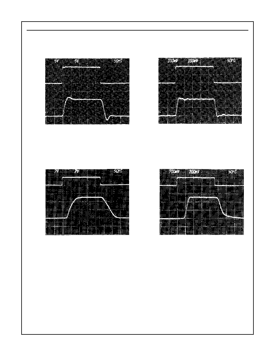
HA2546/883
V
Y
LARGE SIGNAL RESPONSE
Vertical Scale: 5V/Div.
Horizontal Scale: 50ns/Div.
V
Y
SMALL SIGNAL RESPONSE
Vertical Scale: 100mV/Div.
Horizontal Scale: 50ns/Div.
V
X
LARGE SIGNAL RESPONSE
Vertical Scale: 2V/Div.
Horizontal Scale: 50ns/Div.
V
X
SMALL SIGNAL RESPONSE
Vertical Scale: 200mV/Div.
Horizontal Scale: 50ns/Div.
Test Waveforms
(Continued)
+5V
IN
0
-5V
+5V
OUT
0
-5V
100mV
IN
0
-100mV
100mV
OUT
0
-100mV
2V
IN
0
5V
OUT
0
200mV
IN
0
500mV
OUT
0
Spec Number
511050-883

8-9
HA2546/883
Burn-In Circuits
HA-2546/883 CERDIP
NOTES:
C1 = 0.01
µ
F/Socket Min.
C2 = 0.01
µ
F/Socket Min.
D1 = D2 = IN4002 or Equivalent/Board
(V+) - (V-)
= 31V
±
1V
HA-2546/883 CERAMIC LCC
NOTES:
C1 = C2 = 0.01
µ
F/Socket Min.
D1 = D2 = IN4002 or Equivalent/Board
(V+) - (V-)
= 31V
±
1V
D2
14
15
16
9
13
12
11
10
1
2
3
4
5
7
6
8
C2
V-
D1
C1
V+
V
YIO
B
V
YIO
A
NC
V
Y
+
V
Y
-
V
REF
GND
NC
GA A
GA C
V-
V
OUT
NC
V
Z
+
V
Z
-
GA B
V
X
+
NC
V
X
-
V+
4
5
6
7
8
10
11
12
13
9
3
2
1
20
19
16
17
18
15
14
C2
D2
D1
C1
+V
-V
Spec Number
511050-883

8-10
HA2546/883
Simplified Schematic
V
BIAS
V
X
-
GA C
REF
GND
V
X
+
GA A
GA B
+
-
V
Y
-
V
Y
+
V
YIO
B
V
YIO
A
V
BIAS
OUT
V -
V +
1.67k
+
-
V
Z
-
V
Z
+
Spec Number
511050-883
8-11
HA2546/883
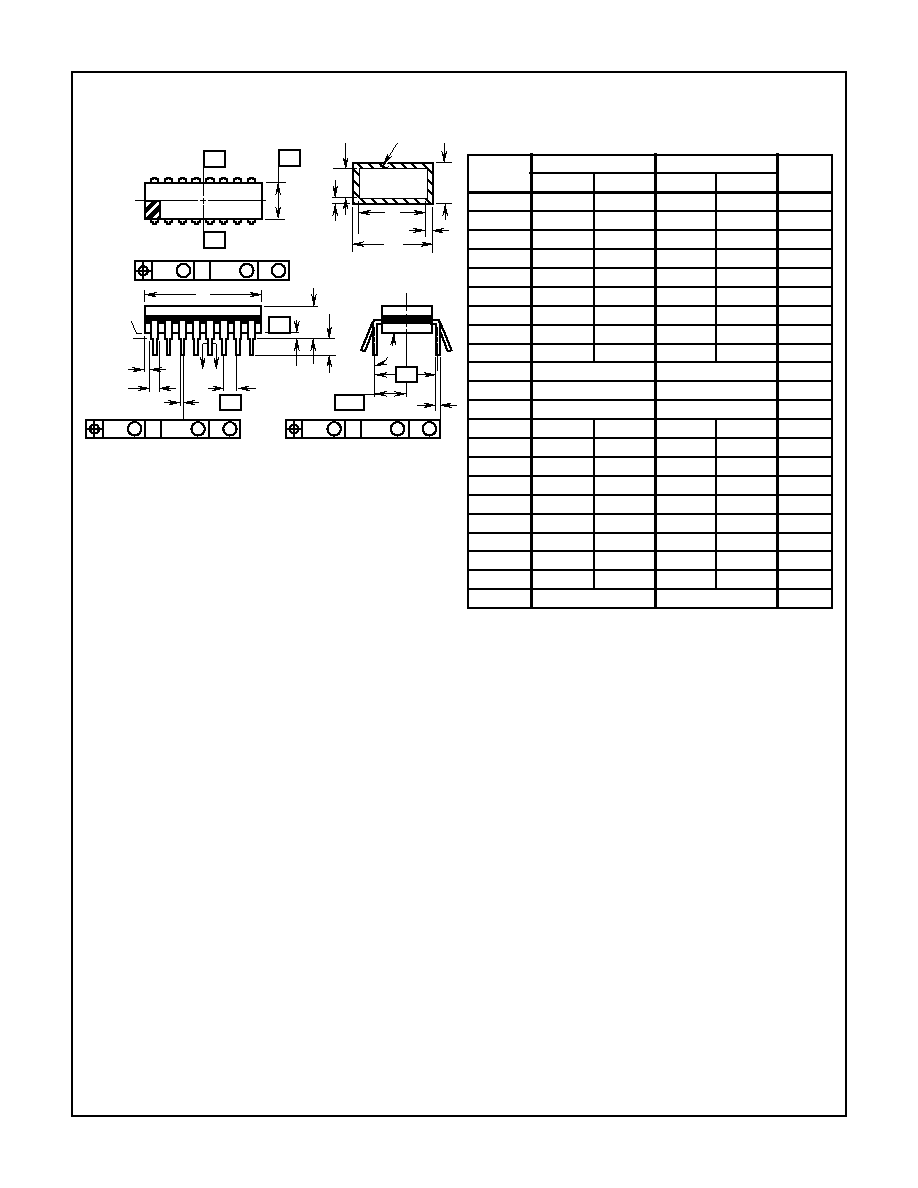
F16.3
MIL-STD-1835 GDIP1-T16 (D-2, CONFIGURATION A)
16 LEAD DUAL-IN-LINE FRIT-SEAL CERAMIC PACKAGE
SYMBOL
INCHES
MILLIMETERS
NOTES
MIN
MAX
MIN
MAX
A
-
0.200
-
5.08
-
b
0.014
0.026
0.36
0.66
2
b1
0.014
0.023
0.36
0.58
3
b2
0.045
0.065
1.14
1.65
-
b3
0.023
0.045
0.58
1.14
4
c
0.008
0.018
0.20
0.46
2
c1
0.008
0.015
0.20
0.38
3
D
-
0.840
-
21.34
5
E
0.220
0.310
5.59
7.87
5
e
0.100 BSC
2.54 BSC
-
eA
0.300 BSC
7.62 BSC
-
eA/2
0.150 BSC
3.81 BSC
-
L
0.125
0.200
3.18
5.08
-
Q
0.015
0.060
0.38
1.52
6
S1
0.005
-
0.13
-
7
S2
0.005
-
0.13
-
-
90
o
105
o
90
o
105
o
-
aaa
-
0.015
-
0.38
-
bbb
-
0.030
-
0.76
-
ccc
-
0.010
-
0.25
-
M
-
0.0015
-
0.038
2
N
16
16
8
NOTES:
1. Index area: A notch or a pin one identification mark shall be locat-
ed adjacent to pin one and shall be located within the shaded
area shown. The manufacturer's identification shall not be used
as a pin one identification mark.
2. The maximum limits of lead dimensions b and c or M shall be
measured at the centroid of the finished lead surfaces, when
solder dip or tin plate lead finish is applied.
3. Dimensions b1 and c1 apply to lead base metal only. Dimension
M applies to lead plating and finish thickness.
4. Corner leads (1, N, N/2, and N/2+1) may be configured with a
partial lead paddle. For this configuration dimension b3 replaces
dimension b1.
5. This dimension allows for off-center lid, meniscus, and glass
overrun.
6. Dimension Q shall be measured from the seating plane to the
base plane.
7. Measure dimension S1 at all four corners.
8. N is the maximum number of terminal positions.
9. Dimensioning and tolerancing per ANSI Y14.5M - 1982.
10. Controlling Dimension: Inch.
11. Materials: Compliant to MIL-I-38535.
bbb
C A - B
S
c
Q
L
A
SEATING
BASE
D
PLANE
PLANE
-D-
-A-
-C-
-B-
D
E
S1
b2
b
A
e
M
c1
b1
(c)
(b)
SECTION A-A
BASE
LEAD FINISH
METAL
e
A/2
A
M
S
S
e
A
ccc
C A - B
M
D
S
S
aaa
C A - B
M
D
S
S
Packaging
Spec Number
511050-883
8-12
HA2546/883
Packaging
(Continued)
D
j x 45
o
D3
B
h x 45
o
A
A1
E
L
L3
e
B3
B1
L1
D2
D1
e
1
E2
E1
L2
PLANE 2
PLANE 1
E3
B2
NOTES:
1. Metallized castellations shall be connected to plane 1 terminals
and extend toward plane 2 across at least two layers of ceramic
or completely across all of the ceramic layers to make electrical
connection with the optional plane 2 terminals.
2. Unless otherwise specified, a minimum clearance of 0.015 inch
(0.381mm) shall be maintained between all metallized features
(e.g., lid, castellations, terminals, thermal pads, etc.)
3. Symbol "N" is the maximum number of terminals. Symbols "ND"
and "NE" are the number of terminals along the sides of length
"D" and "E", respectively.
4. The required plane 1 terminals and optional plane 2 terminals
shall be electrically connected.
5. The corner shape (square, notch, radius, etc.) may vary at the
manufacturer's option, from that shown on the drawing.
6. Chip carriers shall be constructed of a minimum of two ceramic
layers.
7. Maximum limits allows for 0.007 inch solder thickness on pads.
8. Materials: Compliant to MIL-I-38535.
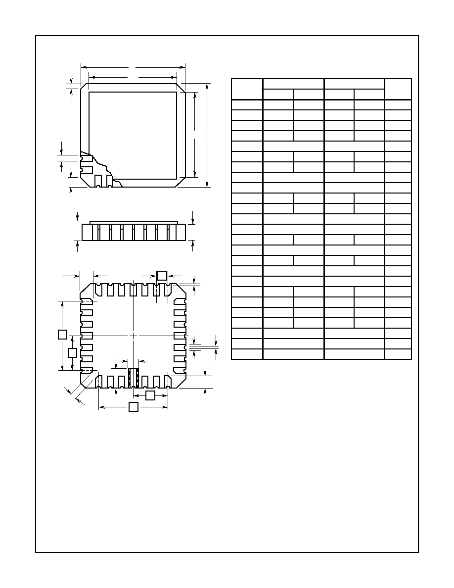
J20.A
MIL-STD-1835 CQCC1-N20 (C-2)
20 PAD METAL SEAL LEADLESS CERAMIC CHIP CARRIER
SYMBOL
INCHES
MILLIMETERS
NOTES
MIN
MAX
MIN
MAX
A
0.060
0.100
1.52
2.54
6, 7
A1
0.050
0.088
1.27
2.23
7
B
-
-
-
-
4
B1
0.022
0.028
0.56
0.71
2, 4
B2
0.072 REF
1.83 REF
-
B3
0.006
0.022
0.15
0.56
-
D
0.342
0.358
8.69
9.09
-
D1
0.200 BSC
5.08 BSC
-
D2
0.100 BSC
2.54 BSC
-
D3
-
0.358
-
9.09
2
E
0.342
0.358
8.69
9.09
-
E1
0.200 BSC
5.08 BSC
-
E2
0.100 BSC
2.54 BSC
-
E3
-
0.358
-
9.09
2
e
0.050 BSC
1.27 BSC
-
e1
0.015
-
0.38
-
2
h
0.040 REF
1.02 REF
5
j
0.020 REF
0.51 REF
5
L
0.045
0.055
1.14
1.40
-
L1
0.045
0.055
1.14
1.40
-
L2
0.075
0.095
1.91
2.41
-
L3
0.003
0.015
0.08
0.38
-
ND
5
5
3
NE
5
5
3
N
20
20
3
Spec Number
511050-883
The information contained in this section has been developed through characterization by Intersil Semiconductor and is for use as
application and design information only. No guarantee is implied.
8-13
DESIGN INFORMATION
August 1999
Semiconductor
HA2546
Wideband Two Quadrant
Analog Multiplier
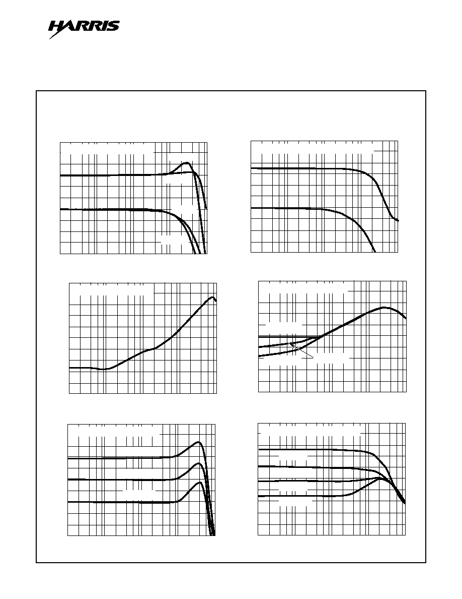
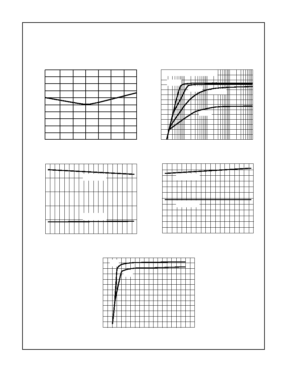
Typical Performance Curves
V
S
=
±
15V, T
A
= +25
o
C, See Test Circuit For Multiplier Configuration.
V
Y
GAIN AND PHASE vs FREQUENCY
V
X
GAIN AND PHASE vs FREQUENCY
V
Y
FEEDTHROUGH vs FREQUENCY
V
X
FEEDTHROUGH vs FREQUENCY
VARIOUS V
Y
FREQUENCY RESPONSES
VARIOUS V
X
FREQUENCY RESPONSES
GAIN (dB)
FREQUENCY (Hz)
9
6
3
0
-3
-6
PHASE SHIFT (DEGREES)
0
45
90
135
180
1M
10M
100M
10K
100K
C
L
= 50pF
C
L
= 50pF
C
L
= 0pF
R
L
= 1K, V
X
= 2V
DC
, V
Y
= 200mVrms
C
L
= 0pF
GAIN (dB)
FREQUENCY (Hz)
PHASE SHIFT (DEGREES)
0
45
90
135
180
1M
10M
100M
10K
100K
-10
10
5
0
-5
15
R
L
= 1K, V
X
+ = 200mVrms, V
Y
= 5V
DC
, V
X
- = -1V
DC
GAIN (dB)
FREQUENCY (Hz)
1M
10M
100M
10K
100K
-10
-20
-30
-40
-50
-60
-70
-80
-90
V
X
= 0V, R
L
= 1K, V
Y
= 200mVrms
(dB)
FREQUENCY (Hz)
1M
10M
100M
10K
100K
-10
-20
-30
-40
-50
0
V
X
= -1.0V
DC
V
X
= -0.5V
DC
V
X
= -2.0V
DC
R
L
= 1K, V
X
+ = 200mVrms, V
Y
= 0V
FREQUENCY (Hz)
1M
10M
100M
10K
100K
V
X
= 1.0V
DC
V
X
= 0.5V
DC
V
X
= 2.0V
DC
GAIN (dB)
-12
-15
9
6
3
0
-3
-6
-9
R
L
= 1K, C
L
= 50pF, V
Y
= 200mVrms
FREQUENCY (Hz)
1M
10M
100M
10K
100K
GAIN (dB)
15
10
5
0
-5
-10
-15
-20
V
Y
= 5V
DC
V
Y
= 2V
DC
V
Y
= 0.5V
DC
V
Y
= 1V
DC
V
X
+ = 200mVrms, R
L
= 1K, V
X
- = -1V
DC
Spec Number
511050-883
DESIGN INFORMATION
(Continued)
The information contained in this section has been developed through characterization by Intersil Semiconductor and is for use as
application and design information only. No guarantee is implied.
8-14
HA2546
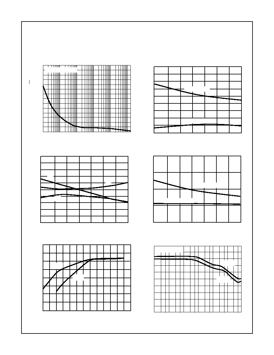
NOISE CHARACTERISTICS
V
Y
OFFSET AND BIAS CURRENT vs TEMPERATURE
OFFSET VOLTAGE vs TEMPERATURE
V
X
OFFSET AND BIAS CURRENT vs TEMPERATURE
V
OUT
vs V
SUPPLY
V
Y
CMRR vs FREQUENCY
Typical Performance Curves
V
S
=
±
15V, T
A
= +25
o
C, See Test Circuit For Multiplier Configuration.
(Continued)
FREQUENCY (Hz)
100
1K
10K
1
10
VOL
T
AGE NOISE (nV/
Hz)
975
900
825
750
675
600
525
450
375
300
225
150
75
0
100K
V
X
= 0V, V
Y
= 0V
14
12
10
-2
-4
8
6
4
2
0
CURRENT (
µ
A)
TEMPERATURE (
o
C)
0
25
50
75
100
125
-55
-25
BIAS CURRENT
OFFSET CURRENT
10
-2
-4
8
6
4
2
0
V
Y
TEMPERATURE (
o
C)
0
25
50
75
100
125
-55
-25
-6
-8
-10
V
X
V
Z
OFFSET VOL
T
AGE (mV)
3
-1
2
1
0
BIAS CURRENT
OFFSET CURRENT
CURRENT (
µ
A)
TEMPERATURE (
o
C)
0
25
50
75
100
125
-55
-25
5
1
4
3
2
-V
OUT
+V
OUT
V
SUPPLY
|V
OUT
| (V)
±
5
±
17
±
15
±
12
±
8
±
7
0
6
7
CMRR (dB)
FREQUENCY (Hz)
1K
10K
100K
1M
10M
100M
100
0
-10
120
100
80
60
40
20
V
X
= 0V
V
X
= 2V
V
Y
CM = 200mVrms
Spec Number
511050-883
DESIGN INFORMATION
(Continued)
The information contained in this section has been developed through characterization by Intersil Semiconductor and is for use as
application and design information only. No guarantee is implied.
8-15
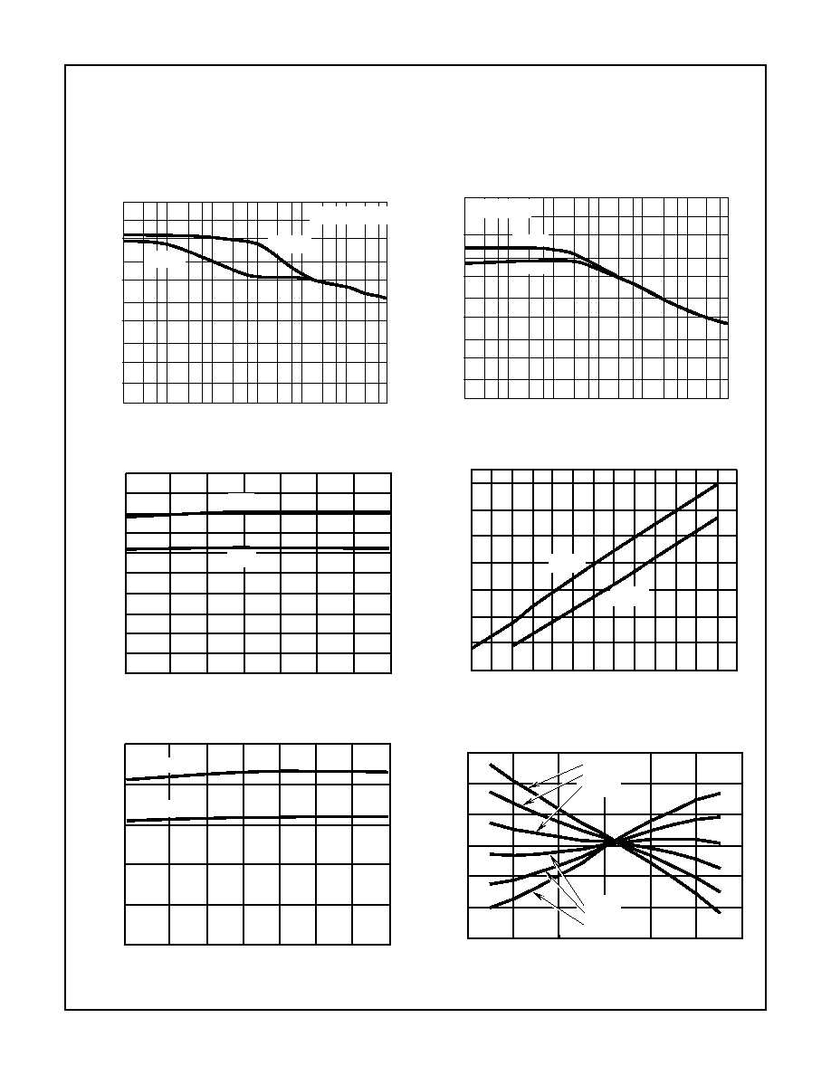
HA2546
V
X
COMMON MODE REJECTION RATIO vs FREQUENCY
PSRR vs FREQUENCY
SUPPLY CURRENT vs TEMPERATURE
COMMON MODE RANGE vs V
SUPPLY
PSRR vs TEMPERATURE
MULTIPLIER ERROR
Typical Performance Curves
V
S
=
±
15V, T
A
= +25
o
C, See Test Circuit For Multiplier Configuration.
(Continued)
CMRR (dB)
FREQUENCY (Hz)
1K
10K
100K
1M
10M
100M
100
V
Y
= 0V
V
Y
= 2V
0
120
100
80
60
40
20
V
X
= 200mVrms
PSRR (dB)
FREQUENCY (Hz)
1K
10K
100K
1M
10M
100M
100
0
100
80
60
40
20
+PSSR
-PSSR
V
Y
= V
X
= 0V
TEMPERATURE (
o
C)
-55
+I
CC
-I
CC
SUPPL
Y CURRENT (mA)
25
20
15
125
-25
0
25
50
75
100
14
6
12
10
8
CMR(-)
±
5
±
17
CMR(+)
|
COMMON MODE RANGE
| (V)
V
SUPPLY
4
2
0
±
15
±
12
±
8
±
7
TEMPERATURE (
o
C)
+PSRR
-PSRR
PSRR (dB)
100
80
60
40
20
0
-55
0
25
50
75
100
125
-25
-6
-4
-2
0
2
4
6
-1.5
-1
-0.5
0
0.5
1
1.5
Y INPUT (V)
MUL
TIPLIER ERROR (%FS)
X = 1
X = 1.2
X = 1.4
X = 1.6
X = 1.8
X = 2
Spec Number
511050-883
DESIGN INFORMATION
(Continued)
The information contained in this section has been developed through characterization by Intersil Semiconductor and is for use as
application and design information only. No guarantee is implied.
8-16
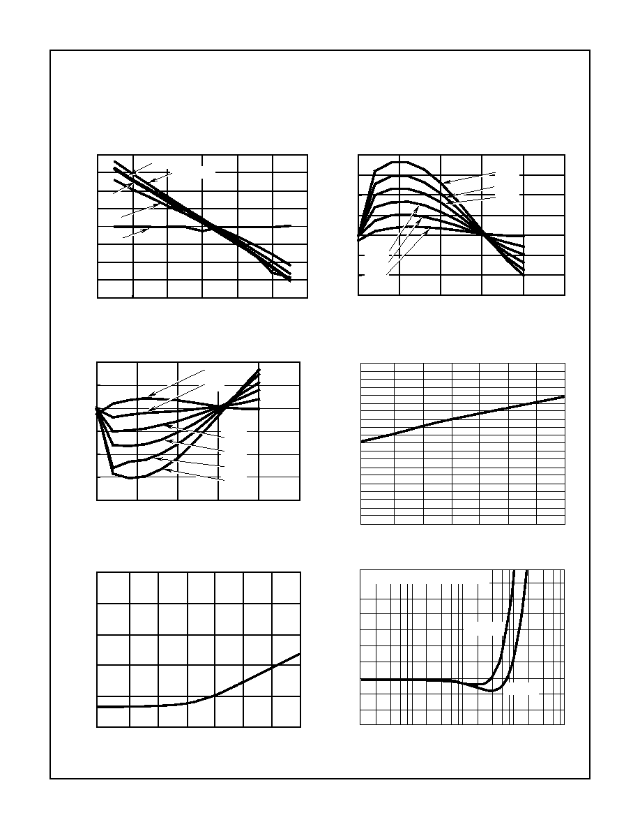
HA2546
MULTIPLIER ERROR
MULTIPLIER ERROR
MULTIPLIER ERROR
WORST CASE MULTIPLICATION ERROR vs
TEMPERATURE
MULTIPLICATION ERROR vs TEMPERATURE
GAIN VARIATION vs FREQUENCY
Typical Performance Curves
V
S
=
±
15V, T
A
= +25
o
C, See Test Circuit For Multiplier Configuration.
(Continued)
-6
-4
-2
0
2
4
6
-2
-1.5
-1
-0.5
0
0.5
1
1.5
2
Y INPUT (V)
MUL
TIPLIER ERROR (%FS)
X = 0
X = 1
X = 0.4, 0.6
X = 0.2
X = 0.8
0
0.5
1
1.5
2
2.5
-1.5
-1
-0.5
0
0.5
1
1.5
2
X INPUT (V)
MUL
TIPLIER ERROR (%FS)
Y = -3
Y = -4
Y = -5
Y = 0
Y = -1
Y = -2
0
0.5
1
1.5
2
2.5
-2
-1.5
-1
-0.5
0
0.5
1
X INPUT (V)
MUL
TIPLIER ERROR (%FS)
Y = 5
Y = 4
Y = 3
Y = 2
Y = 1
Y = 0
TEMPERATURE (
o
C)
MUL
TIPLICA
TION ERROR (%)
2.0
1.9
1.8
1.7
1.6
1.5
1.4
1.3
1.2
1.1
1.0
0.9
0.8
0.7
0.6
0.5
0.4
0.3
0.2
0.1
0.0
0
25
50
75
100
125
-55
-25
TEMPERATURE (
o
C)
MUL
TIPLICA
TION ERROR (%)
0.5
0.4
0.3
0.2
0.1
0.0
-55
0
25
50
75
100
125
-25
GAIN (dB)
FREQUENCY (Hz)
1M
10M
100M
10K
100K
C
L
= 50pF
C
L
= 0pF
0.6
0.4
0.2
0
-0.2
R
L
= 1K, V
X
= 2V
DC
, V
Y
= 200mVrms
Spec Number
511050-883
DESIGN INFORMATION
(Continued)
The information contained in this section has been developed through characterization by Intersil Semiconductor and is for use as
application and design information only. No guarantee is implied.
8-17
HA2546
SCALE FACTOR vs TEMPERATURE
OUTPUT VOLTAGE SWING vs LOAD RESISTANCE
SLEW RATE vs TEMPERATURE
RISE TIME vs TEMPERATURE
SUPPLY CURRENT vs SUPPLY VOLTAGE
Typical Performance Curves
V
S
=
±
15V, T
A
= +25
o
C, See Test Circuit For Multiplier Configuration.
(Continued)
TEMPERATURE (
o
C)
SCALE F
ACT
OR
2.010
2.008
2.006
2.004
2.002
2.000
1.998
1.996
1.994
1.992
1.990
0
25
50
75
100
125
-55
-25
PEAK OUTPUT VOL
T
AGE
1K
10K
100K
10
100
7.0
6.0
5.0
4.0
3.0
2.0
1.0
0.0
LOAD RESISTANCE (
)
V
S
=
±
10
V
S
=
±
15
V
S
=
±
12
V
S
=
±
8
f
O
= 10kHz, V
X
= 2V
DC
, THD < 0.1%
0
20
40
60
80
100
120
-60
-40
-20
TEMPERATURE (
o
C)
500
400
300
200
100
0
SLEW RA
TE (V/
µ
s)
V
Y
CHANNEL
V
X
CHANNEL
TEMPERATURE (
o
C)
V
Y
CHANNEL
V
X
CHANNEL
0
20
40
60
80
100
120
-60
-40
-20
24
22
20
18
16
14
12
10
8
6
4
2
0
RISE TIME (ns)
SUPPL
Y CURRENT (mA)
28
26
24
22
20
18
16
14
12
10
8
6
4
2
0
2
4
6
8
10
12
14
16
18
20
SUPPLY VOLTAGE (
±
V)
+I
CC
-I
CC
Spec Number
511050-883
DESIGN INFORMATION
(Continued)
The information contained in this section has been developed through characterization by Intersil Semiconductor and is for use as
application and design information only. No guarantee is implied.
8-18
HA2546
Application Information
Theory of Operation
The HA-2546 is a two quadrant multiplier with the following
three differential inputs; the signal channel, V
Y
+ and V
Y
-, the
control channel, V
X
+ and V
X
-, and the summed channel,
V
Z
+ and V
Z
-, to complete the feedback of the output ampli-
fier. The differential voltages of channel X and Y are con-
verted to differential currents. These currents are then
multiplied in a circuit similar to a Gilbert Cell multiplier, pro-
ducing a differential current product. The differential voltage
of the Z channel is converted into a differential current which
then sums with the products currents. The differential "prod-
uct/sum" currents are converted to a single-ended current
and then converted to a voltage output by a transimpedance
amplifier.
The open loop transfer equation for the HA-2546 is:
The scale factor is used to maintain the output of the multi-
plier within the normal operating range of
±
5V. The scale fac-
tor can be defined by the user by way of an optional external
resistor, R
EXT
, and the Gain Adjust pins, Gain Adjust A (GA
A), Gain Adjust B (GA B), and Gain Adjust C (GA C). The
scale factor is determined as follows:
The scale factor can be adjusted from 2 to 5. It should be
noted that any adjustments to the scale factor will affect the
AC performance of the control channel, V
X
. The normal input
operating range of V
X
is equal to the scale factor voltage.
The typical multiplier configuration is shown in Figure 1. The
ideal transfer function for this configuration is:
V
OUT
= A
(V
X+
- V
X-
) (V
Y+
- V
Y-
)
SF
- (V
Z+
- V
Z-
)
where;
A = Output Amplifier Open Loop Gain
SF = Scale Factor
V
X
, V
Y
, V
Z
= Differential Inputs
SF = 2, when GA B is shorted to GA C
SF
1.2 R
EXT
, when R
EXT
is connected between
GA A and GA C (R
EXT
is in k
)
SF
1.2 (R
EXT
+ 1.667k
), when R
EXT
is
connected to GA B and GA C (R
EXT
is in k
)
V
OUT
=
(V
X+
- V
X-
) (V
Y+
- V
Y-
)
2
+ V
Z-
, when V
X
0V
0
, when V
X
< 0V
FIGURE 1.
The V
X-
pin is usually connected to ground so that when V
X+
is negative there is no signal at the output, i.e. two quadrant
operation. If the V
X
input is a negative going signal the V
X+
pin maybe grounded and the V
X-
pin used as the control
input.
The V
Y-
terminal is usually grounded allowing the V
Y+
to
swing
±
5V. The V
Z+
terminal is usually connected directly to
V
OUT
to complete the feedback loop of the output amplifier
while V
Z-
is grounded. The scale factor is normally set to 2
by connecting GA B to GA C. Therefore the transfer equation
simplifies to V
OUT
= (V
X
V
Y
) / 2.
Offset Adjustment
The signal channel offset voltage may be nulled by using a
20k
potentiometer between V
YIO
Adjust pins A and B and
connecting the wiper to -V. Reducing the signal channel off-
set will reduce V
X
AC feedthrough. Output offset voltage can
also be nulled by connecting V
Z-
to the wiper of a 20k
potentiometer which is tied between +V and -V.
Capacitive Drive Capability
When driving capacitive loads >20pF, a 50
resistor is rec-
ommended between V
OUT
and V
Z+
, using V
Z+
as the output
(See Figure 1). This will prevent the multiplier from going
unstable.
Power Supply Decoupling
Power supply decoupling is essential for high frequency cir-
cuits. A 0.01
µ
F high quality ceramic capacitor at each supply
pin in parallel with a 1
µ
F tantalum capacitor will provide
excellent decoupling. Chip capacitors produce the best
results due to the close spacing with which they may be
placed to the supply pins minimizing lead inductance.
Adjusting Scale Factor
The HA-2546 two quadrant multiplier may be configured for
many uses. Following are examples of a few typical applica-
tions.
NC
NC
V
Y
+
V-
V
OUT
V+
V
X
+
NC
NC
50
1K
50pF
14
15
16
9
13
12
11
10
1
2
3
4
5
7
6
8
+
-
REF
Y
X
Z
-
+
-
+
-
+
Spec Number
511050-883

DESIGN INFORMATION
(Continued)
The information contained in this section has been developed through characterization by Intersil Semiconductor and is for use as
application and design information only. No guarantee is implied.
8-19
HA2546
Adjusting the scale factor will tailor the control signal, V
X
,
input voltage range to match your needs. Referring to the
simplified schematic and looking for the V
X
input stage, you
will notice the unusual design. The internal reference sets up
a 1.2mA current sink for the V
X
differential pair. The control
signal applied to this input will be forced across the scale
factor setting resistor and set the current flowing in the V
X+
side of the differential pair. When the current through this
resistor reaches 1.2mA, all the current available is flowing in
the one side and full scale has been reached. Normally the
1.67k
internal resistor sets the scale factor to 2V when the
Gain Adjust pins B and C are connected together, but you
may set this resistor to any convenient value using pins 16
(GA A) and 15 (GA C).
FIGURE 2A. MULTIPLIER, V
OUT
= V
X
V
Y
/ 2, SCALE FACTOR = 2V
FIGURE 2B. MULTIPLIER, V
OUT
= V
X
V
Y
/ 5, SCALE FACTOR = 5V
NC
NC
V
Y
+
V-
V
OUT
V+
V
X
+
NC
NC
50
1K
14
15
16
9
13
12
11
10
1
2
3
4
5
7
6
8
+
-
REF
Y
X
Z
-
+
-
+
-
+
NC
NC
V
Y
+
V-
V
OUT
V+
V
X
+
NC
NC
50
1K
14
15
16
9
13
12
11
10
1
2
3
4
5
7
6
8
+
-
REF
Y
X
Z
-
+
-
+
-
+
4.167K
FIGURE 3. AUTOMATIC GAIN CONTROL
In Figure 3, the HA-2546 is configured in a true Automatic
Gain Control or AGC application. The HA-5127, low noise op
amp, provides the gain control level to the X input. This level
will set the peak output voltage of the multiplier to match the
reference level. The feedback network around the HA-5127
provides stability and a response time adjustment for the
gain control circuit.
5k
10k
HA-5127
0.01
µ
F
10k
0.1
µ
F
1N914
3.3V
0.1
µ
F
+15V
20k
NC
NC
V
Y
+
V-
V
OUT
V+
NC
NC
50
14
15
16
9
13
12
11
10
1
2
3
4
5
7
6
8
+
-
REF
Y
X
Z
-
+
-
+
-
+
-
+
Spec Number
511050-883
DESIGN INFORMATION
(Continued)
The information contained in this section has been developed through characterization by Intersil Semiconductor and is for use as
application and design information only. No guarantee is implied.
8-20
HA2546
FIGURE 4A. VOLTAGE CONTROLLED AMPLIFIER
This multiplier has the advantage over other AGC circuits, in
that the signal bandwidth is not affected by the control signal
gain adjustment.
A wide range of gain adjustment is available with the Voltage
Controlled Amplifier configuration shown in Figure 4A. and
Figure 4B. Here the gain of the HFA0002 is swept from 20V/
V at a control voltage of 0.902V to a gain of almost 1000V/V
with a control voltage of 0.03V.
The Video Fader circuit provides a unique function as shown
in Figure 5. Here Ch B is applied to the minus Z input in
addition to the minus Y input. V
MIX
will control the percent-
age of Ch A and Ch B that are mixed together to produce a
resulting video image or other signal.
Many other applications are possible including division,
squaring, square-root, percentage calculations, etc. Please
refer to the HA-2556 four quadrant multiplier for additional
applications.
HFA0002
V
OUT
NC
NC
V-
V+
NC
NC
5k
14
15
16
9
13
12
11
10
1
2
3
4
5
7
6
8
+
-
REF
Y
X
Z
-
+
-
+
-
+
-
+
.
FIGURE 4B. VOLTAGE CONTROLLED AMPLIFIER
FIGURE 5. VIDEO FADER
VOL
T
AGE GAIN (dB)
FREQUENCY (Hz)
100
PHASE (DEGREES)
180
135
90
45
0
100K
10M
100M
1K
10K
V
GAIN
= 0.030V
1M
80
60
40
20
0
-20
-40
-60
-80
-100
0.126V
0.4V
0.902V
REF LEVEL
0.000dB
180.000DEG
/DIV
20.000dB
45.000DEG
MARKET 1000 000.00Hz
MAG (UDF) 56.431dB
MARKER 1000 000.000Hz
PHASE (UDF) 177.646deg
V
OUT
= Ch B + (Ch A - Ch B) V
MIX
/ Scale Factor
Scale Factor = 2
V
OUT
= All Ch B; if V
MIX
= 0V
V
OUT
= All Ch A; if V
MIX
= 2V (Full Scale)
V
OUT
= Mix of Ch A and Ch B; if 0V < V
MIX
< 2V
NC
NC
V-
V
OUT
V+
V
MIX
(0V TO 2V)
NC
NC
50
14
15
16
9
13
12
11
10
1
2
3
4
5
7
6
8
+
-
REF
Y
X
Z
-
+
-
+
-
+
CH A
CH B
Spec Number
511050-883
DESIGN INFORMATION
(Continued)
The information contained in this section has been developed through characterization by Intersil Semiconductor and is for use as
application and design information only. No guarantee is implied.
8-21
HA2546
TYPICAL PERFORMANCE CHARACTERISTICS
Device Tested at: Supply Voltage =
±
15V, R
LOAD
= 1k
, C
LOAD
= 50pF, Unless Otherwise Specified.
PARAMETER
CONDITIONS
TEMP
TYP
UNITS
Multiplication Error Drift
Full
0.002
%/
o
C
Differential Gain
V
X
= 2V, V
Y
= 300mV
P-P
, f
O
= 3.58MHz
+25
o
C
0.1
%
Differential Phase
V
X
= 2V, V
Y
= 300mV
P-P
, f
O
= 3.58MHz
+25
o
C
0.1
Degrees
Gain Tolerance
DC to 5MHz
V
X
= 2V
+25
o
C
0.1
dB
5MHz to 8MHz
+25
o
C
0.18
dB
1% Amplitude Error
+25
o
C
6
MHz
1% Vector Error
+25
o
C
260
kHz
THD+N
f
O
= 10kHz, V
Y
= 1Vrms, V
X
= 2V
+25
o
C
0.03
%
Voltage Noise
f
O
= 10Hz
V
X
= 0V, V
Y
= 0V
+25
o
C
400
nV/Hz
f
O
= 100Hz
+25
o
C
150
nV/Hz
f
O
= 1kHz
+25
o
C
75
nV/Hz
Common Mode Range
+25
o
C
±
9
V
SIGNAL INPUT, V
Y
Average Offset Voltage Drift
Full
45
µ
V/
o
C
Differential Input Resistance
+25
o
C
720
K
Small Signal Bandwidth (-3dB)
V
X
= 2V
+25
o
C
40
MHz
Feedthrough
f
O
= 5MHz, V
X
= 0V, V
Y
= 200mVrms
+25
o
C
-52
dB
V
Y
TRANSIENT RESPONSE
Propagation Delay
+25
o
C
25
ns
Settling Time
V
Y
=
±
5V, V
X
= 2V
+25
o
C
200
ns
CONTROL INPUT, V
X
Average Offset Voltage Drift
Full
10
µ
V/
o
C
Differential Input Resistance
+25
o
C
360
k
Small Signal Bandwidth (-3dB)
V
Y
= 5V, V
X
= -1V
+25
o
C
17
MHz
Feedthrough
f
O
= 100kHz, V
Y
= 0V, V
X
= 200mVrms
+25
o
C
-40
dB
Common Mode Rejection Ratio
V
X
= 0V to 2V, V
Y
= 5V
+25
o
C
80
dB
V
X
TRANSIENT RESPONSE
Propagation Delay
+25
o
C
50
ns
Settling Time
V
X
= 0 to 2V, V
Y
= 5V
+25
o
C
200
ns
V
Z
CHARACTERISTICS
Open Loop Gain
+25
o
C
70
dB
Differential Input Resistance
+25
o
C
900
k
OUTPUT CHARACTERISTICS
Output Resistance
+25
o
C
1
Spec Number
511050-883
All Intersil semiconductor products are manufactured, assembled and tested under ISO9000 quality systems certification.
Intersil products are sold by description only. Intersil Corporation reserves the right to make changes in circuit design and/or specifications at any time without
notice. Accordingly, the reader is cautioned to verify that data sheets are current before placing orders. Information furnished by Intersil is believed to be accurate
and reliable. However, no responsibility is assumed by Intersil or its subsidiaries for its use; nor for any infringements of patents or other rights of third parties which
may result from its use. No license is granted by implication or otherwise under any patent or patent rights of Intersil or its subsidiaries.
For information regarding Intersil Corporation and its products, see web site http://www.intersil.com