Document Outline
- HA-2547
- HA-2547
- 100MHz, Two Quadrant, Current Output, Analog Multiplier
- 0 to 75
- -40 to 85
- HA-2547, (CERDIP)
- Schematic
- 1.� qJA is measured with the component mounted on an evaluation PC board in free air.
- 25
- -
- 1.6
- 3
- %FS
- Full
- -
- 3.0
- 7
- %FS
- Full
- -
- 0.003
- -
- %/oC
- Full
- -
- 0.7
- 5
- %
- 25
- -
- 0.03
- -
- %
- 25
- -
- 6
- 15
- mV
- Full
- -
- 14
- 20
- mV
- Full
- -
- -
- -
- mV/oC
- 25
- -
- 4
- 10
- mV
- Full
- -
- 8
- 20
- mV
- Full
- -
- 35
- -
- mV/oC
- 25
- -
- 7
- 15
- mA
- Full
- -
- 10
- 15
- mA
- 25
- -
- 0.7
- 2
- mA
- Full
- -
- 1.0
- 3
- mA
- 25
- -
- 720
- -
- kW
- 25
- -
- 2.5
- -
- pF
- 25
- -
- 100
- -
- MHz
- 25
- -
- -50
- -
- dB
- 25
- ±5
- -
- -
- V
- 25
- -
- ±9
- -
- V
- Full
- 60
- 78
- -
- dB
- 25
- -
- 5
- -
- ns
- 25
- -
- 3
- -
- ns
- 25
- -
- 1
- 2
- mV
- Full
- -
- 2
- 20
- mV
- Full
- -
- 12
- -
- mV/oC
- 25
- -
- 1.2
- 2
- mA
- Full
- -
- 1.8
- 5
- mA
- 25
- -
- 0.3
- 2
- mA
- Full
- -
- 0.4
- 3
- mA
- 25
- -
- 2.5
- -
- pF
- 25
- -
- 360
- -
- kW
- 25
- -
- 22
- -
- MHz
- 25
- -
- -40
- -
- dB
- Full
- +2
- -
- -
- V
- 25
- -
- ±9
- -
- V
- 25
- -
- 75
- -
- dB
- 25
- -
- 15
- -
- ns
- 25
- -
- 25
- -
- ns
- Full
- -
- ±6.25
- -
- V
- 25
- -
- 2
- -
- mA
- 25
- -
- 6.5
- -
- pF
- 25
- -
- 4
- -
- MW
- Full
- 58
- 63
- -
- dB
- Full
- -
- 20
- 29
- mA
- 2.� Error is percent of full scale, 1% = 50mV.
- 3.� f = 10kHz, VY = 1VRMS�, VX = 2V.
- 4.� VY = 0 to ±5V, VX = 2V.
- 5.� VX = 0 to 2V, VY = 5V.
- 6.� VS = ±12V to ±15V, VY = 5V, VX = 2V.
- 7.� Guaranteed by sample test and not 100% tested.
- 8.� Output current tolerance is ±20%.
- 9.� Scale Factor = 2. See Applications Information.
- 10.� f = 5MHz, VX = 0, VY = 200mVRMS. Relative to full scale output.
- 11.� f = 5MHz, VY = 0, VX+ = 200mVRMS, VX- = -0.5V. Relative to full scale output.
- 12.� VY = ±5V, VX = 2V, RL = 50W.
- 13.� VX = 0 to 2V, VY = 5V, RL = 50W.
- FIGURE 1.� AC AND TRANSIENT RESPONSE TEST CIRCUIT
- Application Information
- HA-2547
- HA-2547
- HA-2547
- HA-2547
- HA-2547
- HA-2547
1
Æ
CAUTION: These devices are sensitive to electrostatic discharge; follow proper IC Handling Procedures.
1-888-INTERSIL or 321-724-7143
|
Intersil (and design) is a registered trademark of Intersil Americas Inc.
Copyright © Intersil Americas Inc. 2002. All Rights Reserved
HA-2547
100MHz, Two Quadrant,
Current Output, Analog Multiplier
The HA-2547 is a monolithic, high speed, two quadrant,
analog multiplier constructed in Intersil's Dielectrically
Isolated High Frequency Process. The high frequency
performance of the HA-2547 rivals the best analog
multipliers currently available including hybrids.
The single-ended current output of the HA-2547 has a
100MHz signal bandwidth (R
L
= 50
) and a 22MHz control
input bandwidth. High bandwidth and low distortion make this
part an ideal component in video systems. The suitability for
precision video applications is demonstrated further by low
multiplication error (1.6%), low feedthrough (-50dB), and
differential inputs with low bias currents (1.2
µA). The HA-2547
is also well suited for mixer circuits as well as AGC
applications for sonar, radar, and medical imaging equipment.
The current output of the HA-2547 allows it to achieve higher
bandwidths than voltage output multipliers. An internal
feedback resistor is provided to give an accurate current-to-
voltage conversion and is trimmed to give a full scale output
voltage of
±5V. The HA-2547 is not limited to multiplication
applications only; frequency doubling and power detection
are also possible.
Features
∑ Low Multiplication Error . . . . . . . . . . . . . . . . . . . . . . . 1.6%
∑ Input Bias Currents . . . . . . . . . . . . . . . . . . . . . . . . . 1.2
µA
∑ Signal Input Feedthrough at 5MHz . . . . . . . . . . . . . -50dB
∑ Wide Signal Bandwidth . . . . . . . . . . . . . . . . . . . . 100MHz
∑ Wide Control Bandwidth. . . . . . . . . . . . . . . . . . . . . 22MHz
Applications
∑ Military Avionics
∑ Missile Guidance Systems
∑ Medical Imaging Displays
∑ Video Mixers
∑ Sonar AGC Processors
∑ Radar Signal Conditioning
∑ Voltage Controlled Amplifier
∑ Vector Generator
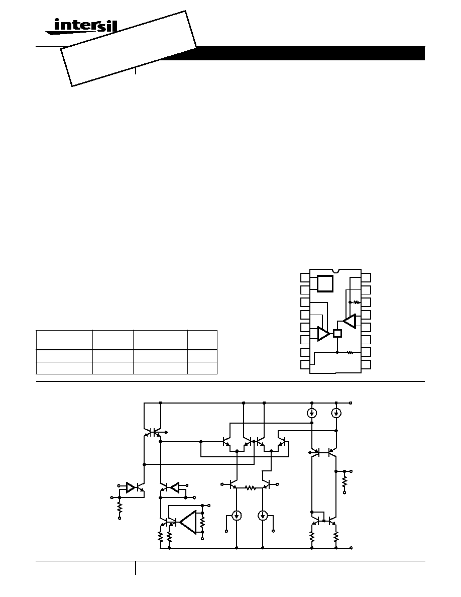
Pinout
HA-2547, (CERDIP)
TOP VIEW
Schematic
Part Number Information
PART NUMBER
TEMP.
RANGE (
o
C)
PACKAGE
PKG.
NO.
HA1-2547-5
0 to 75
16 Ld CERDIP
F16.3
HA1-2547-9
-40 to 85
16 Ld CERDIP
F16.3
15
16
9
13
12
11
10
1
2
3
4
5
7
6
8
REF
GND
V-
I
OUT
V
YIO
B
V
YIO
A
V
Y
+
GA A
GA C
GA B
V+
V
X
-
NC
R
Z
V
X
+
X
V
REF
V
Y
-
14
V
BIAS
V
X
-
GA A
GA B
GA C
GND
V
YIO
A
V
YIO
B
V
X
+
V
Y
+
V+
V
REF
V
BIAS
R
Z
V
OUT
V
Y
-
+
-
+
-
+
-
V-
September 1998
File Number 2862.3
OBSO
LETE
PRO
DUCT
See H
A-254
6
conta
ct ou
r Tec
hnica
l Sup
port C
enter
at
1-888
-INTE
RSIL
or ww
w.inte
rsil.c
om/ts
c
2
Absolute Maximum Ratings
Thermal Information
Voltage Between V+ and V- Terminals . . . . . . . . . . . . . . . . . . . 35V
Differential Input Voltage . . . . . . . . . . . . . . . . . . . . . . . . . . . . . . . 6V
Output Current . . . . . . . . . . . . . . . . . . . . . . . . . . . . . . . . . . . . . . 3mA
Operating Conditions
Temperature Range
HA-2547-9 . . . . . . . . . . . . . . . . . . . . . . . . . . . . . . . -40
o
C to 85
o
C
HA-2547-5 . . . . . . . . . . . . . . . . . . . . . . . . . . . . . . . . 0
o
C to 75
o
C
Thermal Resistance (Typical, Note 1)
JA
(
o
C/W)
JC
(
o
C/W)
CERDIP Package. . . . . . . . . . . . . . . . .
75
20
Maximum Junction Temperature . . . . . . . . . . . . . . . . . . . . . . . 175
o
C
Maximum Storage Temperature Range . . . . . . . . . -65
o
C to 150
o
C
Maximum Lead Temperature (Soldering 10s) . . . . . . . . . . . . 300
o
C
CAUTION: Stresses above those listed in "Absolute Maximum Ratings" may cause permanent damage to the device. This is a stress only rating and operation of the
device at these or any other conditions above those indicated in the operational sections of this specification is not implied.
NOTE:
1.
JA
is measured with the component mounted on an evaluation PC board in free air.
Electrical Specifications
V
SUPPLY
=
±15V, R
Z
(Pin 10) Grounded, Unless Otherwise Specified. Pin 14 Connected to Pin 15 for Scale
Factor = 2
PARAMETER
TEST CONDITIONS
TEMP. (
o
C)
MIN
TYP
MAX
UNITS
MULTIPLIER PERFORMANCE
Multiplication Error (Note 2)
25
-
1.6
3
%FS
Full
-
3.0
7
%FS
Multiplication Error Drift
Full
-
0.003
-
%/
o
C
Scale Factor Error
Full
-
0.7
5
%
THD+N
Note 3
25
-
0.03
-
%
Output Offset Voltage
V
X
= 0V, V
Y
= 0V
25
-
6
15
mV
Full
-
14
20
mV
Average Offset Voltage Drift
Full
-
-
-
µV/
o
C
SIGNAL INPUT, V
Y
Input Offset Voltage
25
-
4
10
mV
Full
-
8
20
mV
Average Offset Voltage Drift
Full
-
35
-
µV/
o
C
Input Bias Current
25
-
7
15
µA
Full
-
10
15
µA
Input Offset Current
25
-
0.7
2
µA
Full
-
1.0
3
µA
Input Differential Resistance
25
-
720
-
k
Input Capacitance
25
-
2.5
-
pF
Small Signal Bandwidth (-3dB) (Note 7)
R
L
= 50
25
-
100
-
MHz
Feedthrough
Note 10
25
-
-50
-
dB
Differential Input Range
25
±5
-
-
V
Common Mode Range
25
-
±9
-
V
CMRR
Note 4
Full
60
78
-
dB
V
Y
TRANSIENT RESPONSE
Rise Time
Note 12
25
-
5
-
ns
Propagation Delay
25
-
3
-
ns
HA-2547

3
CONTROL INPUT, V
X
Input Offset Voltage
25
-
1
2
mV
Full
-
2
20
mV
Average Offset Voltage Drift
Full
-
12
-
µV/
o
C
Input Bias Current
25
-
1.2
2
µA
Full
-
1.8
5
µA
Input Offset Current
25
-
0.3
2
µA
Full
-
0.4
3
µA
Input Capacitance
25
-
2.5
-
pF
Input Differential Resistance
25
-
360
-
k
Small Signal Bandwidth (-3dB) (Note 7)
R
L
= 50
25
-
22
-
MHz
Feedthrough
Note 11
25
-
-40
-
dB
Input Range (Note 9)
Full
+2
-
-
V
Common Mode Range
25
-
±9
-
V
CMRR
Note 5
25
-
75
-
dB
V
X
TRANSIENT RESPONSE
Rise Time
Note 13
25
-
15
-
ns
Propagation Delay
25
-
25
-
ns
OUTPUT CHARACTERISTICS
Full Scale Output Voltage
V
Y
=
±5V, V
X
= 2.5V
Full
-
±6.25
-
V
Full Scale Output Current (Note 8)
25
-
2
-
mA
Output Capacitance
25
-
6.5
-
pF
Output Resistance
25
-
4
-
M
POWER SUPPLY
PSRR
Note 6
Full
58
63
-
dB
I
CC
Full
-
20
29
mA
NOTES:
2. Error is percent of full scale, 1% = 50mV.
3. f = 10kHz, V
Y
= 1V
RMS
, V
X
= 2V.
4. V
Y
= 0 to
±5V, V
X
= 2V.
5. V
X
= 0 to 2V, V
Y
= 5V.
6. V
S
=
±12V to ±15V, V
Y
= 5V, V
X
= 2V.
7. Guaranteed by sample test and not 100% tested.
8. Output current tolerance is
±20%.
9. Scale Factor = 2. See Applications Information.
10. f = 5MHz, V
X
= 0, V
Y
= 200mV
RMS
. Relative to full scale output.
11. f = 5MHz, V
Y
= 0, V
X
+ = 200mV
RMS
, V
X
- = -0.5V. Relative to full scale output.
12. V
Y
=
±5V, V
X
= 2V, R
L
= 50
.
13. V
X
= 0 to 2V, V
Y
= 5V, R
L
= 50
.
Electrical Specifications
V
SUPPLY
=
±15V, R
Z
(Pin 10) Grounded, Unless Otherwise Specified. Pin 14 Connected to Pin 15 for Scale
Factor = 2 (Continued)
PARAMETER
TEST CONDITIONS
TEMP. (
o
C)
MIN
TYP
MAX
UNITS
HA-2547

4
Application Information
Theory of Operation
The HA-2547 is a current output, two quadrant multiplier with
one differential signal channel, V
Y
+ and V
Y
-, and one
differential control channel, V
X
+ and V
X
-. Figure 2 shows a
detailed functional block diagram of the HA-2547. The
differential voltages of channels V
X
and V
Y
are converted to
differential currents. These differential currents are then
multiplied in a circuit similar to a Gilbert Cell multiplier,
producing a differential current product. The differential
product currents are then converted to a single-ended output
current which is typically 2mA,
±20% at full scale (V
X
= 2V,
V
Y
=
±5V). A trimmed internal scaling resistor, R
Z
, is
designed to convert the output current to an accurate voltage
by grounding R
Z
(pin 10). R
Z
is trimmed such that at full scale
output current the voltage drop across R
Z
will be
±5.0V.
Test Circuits and Waveforms
FIGURE 1. AC AND TRANSIENT RESPONSE TEST CIRCUIT
Horizontal Scale: 20ns/Div.
V
Y
TRANSIENT RESPONSE
Horizontal Scale: 50ns/Div.
V
X
TRANSIENT RESPONSE
14
15
16
9
13
12
11
10
1
2
3
4
5
7
6
8
+15V
V
OUT
NC
NC
NC
-15V
50
NC
V
Y
+
V
X
+
X
REF
NC
NC
+5V
IN 0V
-5V
100mV
OUT 0V
-100mV
2V
IN 0V
100mV
OUT 0V
GA A
GA B
GA C
1.67K
V
YIO
A
V
YIO
B
V
Y
V
X
MULTIPLIER
CORE
V
REF
STABLE
REFERENCE
AND BIAS
V+
V-
R
Z
2.5K
+
+
+
I
OUT
FIGURE 2.
HA-2547
5
The transfer equation for the HA-2547 is:
SF = Scale Factor
R
Z
= 2.5kV (Internal)
V
X
, V
Y
= Differential Inputs
The scale factor is used to maintain the output of the
multiplier within the normal operating range of
±5V. The
scale factor can be defined by the user by way of an optional
external resistor, R
EXT
, and the Gain Adjust pins: Gain
Adjust A (GA A), Gain Adjust B (GA B), and Gain Adjust C
(GA C). The scale factor is determined as follows:
SF = 2, when GA B is shorted to GA C
SF
(1.2)(R
EXT
), when R
EXT
is connected between GA A
and GA C (R
EXT
is in k
)
SF
(1.2)(R
EXT
+ 1.667k
), when R
EXT
is connected to
GA B and GA C (R
EXT
is in k
).
The scale factor can be adjusted from 2 to 5. It should be
noted that any adjustments to the scale factor will affect the
AC performance of the control channel, V
X
. The normal
input operating range of V
X
is equal to the scale factor value.
A typical multiplier configuration is shown in Figure 3. The
ideal transfer function for this configuration is shown below,
illustrating two quadrant operation:
The V
X
- pin is usually connected to ground so that when
V
X
+ is negative there is no signal at the output, i.e. two
quadrant operation. If the V
X
input is a negative going signal
the V
X
+ pin maybe grounded and the V
X
- pin used as the
input. The V
Y
- terminal is usually grounded allowing V
Y
+ to
swing
±5V. R
Z
is normally used as a feedback resistor for an
external op amp to provide an accurate current-to-voltage
conversion. The scale factor is normally set to 2 by
connecting GA B to GA C. Therefore, the transfer function
becomes:
The multiplication error is trimmed to be minimum at full
scale, V
X
= 2V and V
Y
=
±5V. When V
Y
=
±5V, the worst
case multiplication error occurs when V
X
0.8V (Refer to
typical performance curves).
Operation At Various Supply Voltages
The HA-2547 will operate over a range of supply voltages,
±8V to ±15V. Use of supply voltages below ±12V will cause
degradation of electrical parameters.
Offset Adjustment
The signal channel offset voltage may be nulled by using a
20K potentiometer between V
YIO
Adjust pins A and B and
connecting the wiper to V-. Reducing the signal channel
offset voltage will reduce V
X
AC feedthrough and improve
the multiplication error.
I
OUT
V
OUT
R
Z
----------------
V
X+
V
X-
≠
(
) V
Y+
V
Y-
≠
(
)
SF R
Z
◊
----------------------------------------------------------------, where
=
=
when V
X+
V
X-
≠
(
) 0
V
OUT
0,
=
when V
X+
V
X-
≠
(
) 0
<
V
OUT
V
X+
V
X-
≠
(
) V
Y+
V
Y-
≠
(
)
2
---------------------------------------------------------------- ,
=
VOUT
VX+
(
) VY+
(
)
2
----------------------------------
=
14
15
16
9
13
12
11
10
1
2
3
4
5
7
6
8
+15V
V
X
REF
-
+
-15V
+15V
-15V
V
Y
V
OUT
R
L
-
+
-
+
X
FIGURE 3.
HA-2547

6
Typical Performance Curves
V
S
=
±15V, T
A
= 25
o
C
FIGURE 4. V
Y
vs FREQUENCY
FIGURE 5. V
X
vs FREQUENCY
FIGURE 6. V
Y
FEEDTHROUGH vs FREQUENCY
FIGURE 7. V
X
FEEDTHROUGH vs FREQUENCY
FIGURE 8. VARIOUS V
Y
FREQUENCY RESPONSES
FIGURE 9. VARIOUS V
X
FREQUENCY RESPONSES
P
HAS
E
S
H
IF
T
(
D
E
G
RE
E
S
)
0
45
90
135
180
1M
10M
100M
10K
100K
FREQUENCY (Hz)
GAIN
PHASE
-30
-35
-40
-45
-50
G
A
IN (
d
B)
V
Y
= 200mV
RMS
, V
X
= 2V, R
L
= 50
1M
10M
100M
10K
100K
FREQUENCY (Hz)
GA
I
N
(d
B
)
-20
-25
-30
-35
-40
-45
-50
-55
P
HAS
E
S
H
IF
T
(
D
E
G
RE
E
S
)
0
45
90
135
180
GAIN
PHASE
V
X
+ = 100mV
RMS
,V
X
- = -1V, V
Y
= 5V, R
L
= 50
-20
V
Y
= 200mV
RMS
, V
X
- = 0V, R
L
= 50
1M
10M
100M
10K
100K
FREQUENCY (Hz)
G
A
IN (
d
B)
-15
-35
-55
-75
-95
-115
-135
V
X
+ = 200mV
RMS
, V
X
- = 0.5V, V
Y
= 0V, R
L
= 50
1M
10M
100M
10K
100K
FREQUENCY (Hz)
G
A
IN (
d
B)
-25
-35
-45
-55
-65
-75
-85
V
Y
= 200mV
RMS
, R
L
= 50
1M
10M
100M
10K
100K
FREQUENCY (Hz)
GA
I
N
(d
B
)
-35
-30
-45
-50
-55
-60
-65
-40
V
X
= 0.25V
V
X
= 1V
V
X
= 2V
V
X
= 0.5V
V
X
+ = 100mV
RMS
, V
X
- = -1V, R
L
= 50
1M
10M
100M
10K
100K
FREQUENCY (Hz)
G
A
IN (
d
B)
-25
-20
-35
-40
-45
-50
-55
-30
V
Y
= 1V
V
Y
= 0.25V
V
Y
= 5V
V
Y
= 2V
V
Y
= 0.5V
HA-2547

7
FIGURE 10. OUTPUT VOLTAGE SWING vs TEMPERATURE
FIGURE 11. OFFSET VOLTAGE vs TEMPERATURE
FIGURE 12. V
Y
OFFSET/BIAS CURRENT vs TEMPERATURE
FIGURE 13. V
X
OFFSET/BIAS CURRENT vs TEMPERATURE
FIGURE 14. SIGNAL/CONTROL CMRR vs TEMPERATURE
FIGURE 15. PSRR vs TEMPERATURE
Typical Performance Curves
V
S
=
±15V, T
A
= 25
o
C (Continued)
TEMPERATURE (
o
C)
P
E
AK O
U
T
P
UT
V
O
L
T
AG
E
S
W
ING
(
±
V)
6
4
2
0
8
0
25
50
75
100
125
-55
-25
V
OUT
O
F
F
S
ET
V
O
L
T
A
G
E (
m
V)
10
6
2
-2
-6
-10
V
X
V
Y
TEMPERATURE (
o
C)
0
25
50
75
100
125
-55
-25
15
10
0
-5
-10
-15
5
CURRE
NT
(
µ
A)
BIAS CURRENT
OFFSET CURRENT
TEMPERATURE (
o
C)
0
25
50
75
100
125
-55
-25
TEMPERATURE (
o
C)
0
25
50
75
100
125
-55
-25
2.0
0
1.0
-1.0
-2.0
CURRE
NT
(
µ
A)
OFFSET CURRENT
BIAS CURRENT
SIGNAL
CONTROL
100
80
40
20
0
60
CM
RR (
d
B)
TEMPERATURE (
o
C)
0
25
50
75
100
125
-55
-25
TEMPERATURE (
o
C)
0
25
50
75
100
125
-55
-25
100
80
40
20
0
60
P
S
RR (
d
B)
+PSRR
-PSRR
HA-2547

8
FIGURE 16. I
CC
vs TEMPERATURE
FIGURE 17. SCALE FACTOR vs TEMPERATURE
FIGURE 18. WORST CASE MULTIPLICATION ERROR vs
TEMPERATURE
FIGURE 19. MULTIPLICATION ERROR vs TEMPERATURE
FIGURE 20. MULTIPLICATION ERROR vs V
X
FIGURE 21. VOLTAGE NOISE DENSITY
Typical Performance Curves
V
S
=
±15V, T
A
= 25
o
C (Continued)
TEMPERATURE (
o
C)
0
25
50
75
100
125
-55
-25
S
U
P
P
L
Y
CURRE
NT
(
m
A)
25
20
15
+I
CC
-I
CC
TEMPERATURE (
o
C)
0
25
50
75
100
125
-55
-25
S
CAL
E
F
A
CT
O
R
2.05
2.04
2.03
2.02
2.01
2.00
1.99
1.98
1.97
1.96
1.95
TEMPERATURE (
o
C)
0
25
50
75
100
125
-55
-25
1.8
1.4
0.8
W
O
RS
T
CAS
E
E
RRO
R (
%
)
ERROR
1.6
1.2
1.0
TEMPERATURE (
o
C)
0
25
50
75
100
125
-55
-25
1.4
1.3
1.2
1.1
1.0
0.9
0.8
0.7
0.6
0.5
0.4
0.3
0.2
0.1
0.0
M
U
L
T
IP
L
I
CAT
IO
N E
RRO
R (
%
)
V
X
VOLTAGE (V)
M
U
L
T
IP
L
I
CAT
IO
N E
RRO
R (
%
)
0.0
0.2
0.4
0.6
0.8
1.0
1.2
1.4
1.6
1.8
2.0
0.2
0.4
0.6
0.8
1.0
1.2
1.4
1.6
1.8
2.0
V
Y
= -5V
V
Y
= +5V
V
X
= 0, V
Y
= 0
1K
10K
100K
1
100
FREQUENCY (Hz)
N
O
I
S
E V
O
L
T
A
G
E (
n
V/
Hz
)
975
900
825
750
675
600
525
10
450
375
300
225
150
75
0
HA-2547