
8-7
CAUTION: These devices are sensitive to electrostatic discharge; follow proper IC Handling Procedures.
http://www.intersil.com or 407-727-9207
|
Copyright
©
Intersil Corporation 1999
HA2556/883
Wideband Four Quadrant Analog
Multiplier (Voltage Output)
Description
The HA-2556/883 is a monolithic, high speed, four quadrant,
analog multiplier constructed in Intersil' Dielectrically
Isolated High Frequency Process. The voltage output
simplifies many designs by eliminating the current-to-voltage
conversion stage required for current output multipliers. The
HA-2556/883 provides a 450V/
µ
s output slew rate and
maintains 52MHz and 57MHz bandwidths for the X and Y
channels respectively, making it an ideal part for use in video
systems.
The suitability for precision video applications is
demonstrated further by the Y Channel 0.1dB gain flatness
to 5.0MHz, 1.5% multiplication error, -50dB feedthrough and
differential inputs with 8
µ
A bias current. The HA-2556 also
has low differential gain (0.1%) and phase (0.1
o
) errors.
The HA-2556/883 is well suited for AGC circuits as well as
mixer applications for sonar, radar, and medical imaging
equipment. The HA-2556/883 is not limited to multiplication
applications only; frequency doubling, power detection, as
well as many other configurations are possible.
Ordering Information
PART NUMBER
TEMPERATURE
RANGE
PACKAGE
HA1-2556/883
-55
o
C to +125
o
C
16 Lead CerDIP
Features
∑ This Circuit is Processed in Accordance to MIL-STD-
883 and is Fully Conformant Under the Provisions of
Paragraph 1.2.1.
∑ High Speed Voltage Output. . . . . . . . . . . 450V/
µ
s (Typ)
∑ Low Multiplication error . . . . . . . . . . . . . . . . 1.5% (Typ)
∑ Input Bias Currents . . . . . . . . . . . . . . . . . . . . . 8
µ
A (Typ)
∑ Signal Input Feedthrough . . . . . . . . . . . . . . -50dB (Typ)
∑ Wide Y Channel Bandwidth . . . . . . . . . . . 57MHz (Typ)
∑ Wide X Channel Bandwidth . . . . . . . . . . . 52MHz (Typ)
∑ 0.1dB Gain Flatness (V
Y
). . . . . . . . . . . . . . 5.0MHz (Typ)
Applications
∑ Military Avionics
∑ Missile Guidance Systems
∑ Medical Imaging Displays
∑ Video Mixers
∑ Sonar AGC Processors
∑ Radar Signal Conditioning
∑ Voltage Controlled Amplifier
∑ Vector Generator
July 1994
Pinout
HA-2556/883
(CERDIP)
TOP VIEW
Simplified Schematic
14
15
16
9
13
12
11
10
1
2
3
4
5
7
6
8
GND
V
REF
V
YIO
B
V
YIO
A
V
Y
+
V
Y
-
V
OUT
V-
V
XIO
A
NC
V
X
+
V
X
-
V+
V
Z
-
V
Z
+
V
XIO
B
+
-
REF
Y
X
Z
V
BIAS
OUT
V
Z
-
V+
V
Z
+
V-
V+
V
YIO
A
V
YIO
B
V
Y
-
V
Y
+
V
XIO
A
V
XIO
B
V
X
+
REF
GND
VBIAS
V
X
-
+
-
Spec Number
511063-883
File Number
3619

8-8
Specifications HA2556/883
Absolute Maximum Ratings
Thermal Information
Voltage Between V+ and V- . . . . . . . . . . . . . . . . . . . . . . . . . . . . 35V
Differential Input Voltage . . . . . . . . . . . . . . . . . . . . . . . . . . . . . . . 6V
Output Current
. . . . . . . . . . . . . . . . . . . . . . . . . . . . . . . . . . . . . . . .±
40mA
ESD Rating. . . . . . . . . . . . . . . . . . . . . . . . . . . . . . . . . . . . . . < 2000V
Lead Temperature (Soldering 10s) . . . . . . . . . . . . . . . . . . . . +300
o
C
Storage Temperature Range . . . . . . . . . . . . . . -65
o
C
T
A
+150
o
C
Max Junction Temperature . . . . . . . . . . . . . . . . . . . . . . . . . . +175
o
C
Thermal Resistance
JA
JC
CerDIP Package . . . . . . . . . . . . . . . . . . .
82
o
C/W
27
o
C/W
Maximum Package Power Dissipation at +75
o
C
CerDIP Package . . . . . . . . . . . . . . . . . . . . . . . . . . . . . . . . . 1.22W
Package Power Dissipation Derating Factor above +75
o
C
CerDIP Package . . . . . . . . . . . . . . . . . . . . . . . . . . . . . . 12mW/
o
C
CAUTION: Stresses above those listed in "Absolute Maximum Ratings" may cause permanent damage to the device. This is a stress only rating and operation
of the device at these or any other conditions above those indicated in the operational sections of this specification is not implied.
Operating Conditions
Operating Supply Voltage (
±
V
S
)
. . . . . . . . . . . . . . . . . . . . . . . . . . ±
15V
Operating Temperature Range . . . . . . . . . . . . -55
o
C
T
A
+125
o
C
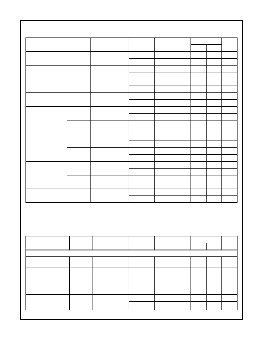
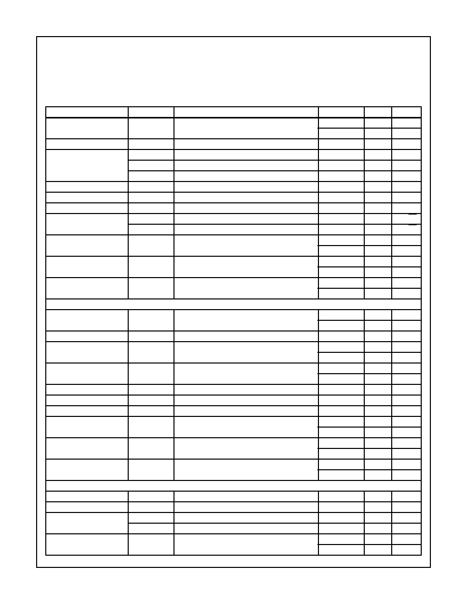
TABLE 1. DC ELECTRICAL PERFORMANCE CHARACTERISTICS
Device Tested at: V
SUPPLY
=
±
15V, R
F
= 50
, R
L
= 1k
, C
L
= 20pF, Unless Otherwise Specified.
PARAMETERS
SYMBOL
CONDITIONS
GROUP A
SUBGROUPS
TEMPERATURE
LIMITS
UNITS
MIN
MAX
Multiplication Error
ME
V
Y
, V
X
=
±
5V
1
+25
o
C
-3
3
%FS
2, 3
+125
o
C, -55
o
C
-6
6
%FS
Linearity Error
LE4V
V
Y
, V
X
=
±
4V
1
+25
o
C
-0.5
0.5
%FS
LE5V
V
Y
, V
X
=
±
5V
1
+25
o
C
-1
1
%FS
Input Offset Voltage (V
X
)
V
XIO
V
Y
=
±
5V
1
+25
o
C
-15
15
mV
2, 3
+125
o
C, -55
o
C
-25
25
mV
Input Bias Current (V
X
)
I
B
(V
X
)
V
X
= 0V, V
Y
= 5V
1
+25
o
C
-15
15
µ
A
2, 3
+125
o
C, -55
o
C
-25
25
µ
A
Input Offset Current (V
X
)
I
IO
(V
X
)
V
X
= 0V, V
Y
= 5V
1
+25
o
C
-2
2
µ
A
2, 3
+125
o
C, -55
o
C
-3
3
µ
A
Common Mode (V
X
)
Rejection Ratio
CMRR (V
X
)
V
X
CM =
±
10V
V
Y
= 5V
1
+25
o
C
65
-
dB
2, 3
+125
o
C, -55
o
C
65
-
dB
Power Supply (V
X
)
Rejection Ratio
+PSRR (V
X
)
V
CC
= +12V to +17V
V
Y
= 5V
1
+25
o
C
65
-
dB
2, 3
+125
o
C, -55
o
C
65
-
dB
-PSRR (V
X
)
V
EE
= -12V to -17V
V
Y
= 5V
1
+25
o
C
45
-
dB
2, 3
+125
o
C, -55
o
C
45
-
dB
Input Offset Voltage (V
Y
)
V
YIO
V
X
=
±
5V
1
+25
o
C
-15
15
mV
2, 3
+125
o
C, -55
o
C
-25
25
mV
Input Bias Current (V
Y
)
I
B
(V
Y
)
V
Y
= 0V, V
X
= 5V
1
+25
o
C
-15
15
µ
A
2, 3
+125
o
C, -55
o
C
-25
25
µ
A
Input Offset Current (V
Y
)
I
IO
(V
Y
)
V
Y
= 0V, V
X
= 5V
1
+25
o
C
-2
2
µ
A
2, 3
+125
o
C, -55
o
C
-3
3
µ
A
Common Mode (V
Y
)
Rejection Ratio
CMRR (V
Y
)
V
Y
CM = +9V, -10V
V
X
= 5V
1
+25
o
C
65
-
dB
2, 3
+125
o
C, -55
o
C
65
-
dB
Power Supply (V
Y
)
Rejection Ratio
+PSRR (V
Y
)
V
CC
= +12V to +17V
V
X
= 5V
1
+25
o
C
65
-
dB
2, 3
+125
o
C, -55
o
C
65
-
dB
-PSRR (V
Y
)
V
EE
= -12V to -17V
V
X
= 5V
1
+25
o
C
45
-
dB
2, 3
+125
o
C, -55
o
C
45
-
dB
Spec Number
511063-883
8-9
Specifications HA2556/883
Input Offset Voltage (V
Z
)
V
ZIO
V
X
= 0V, V
Y
= 0V
1
+25
o
C
-15
15
mV
2, 3
+125
o
C, -55
o
C
-25
25
mV
Input Bias Current (V
Z
)
I
B
(V
Z
)
V
X
= 0V, V
Y
= 0V
1
+25
o
C
-15
15
µ
A
2, 3
+125
o
C, -55
o
C
-25
25
µ
A
Input Offset Current (V
Z
)
I
IO
(V
Z
)
V
X
= 0V, V
Y
= 0V
1
+25
o
C
-2
2
µ
A
2, 3
+125
o
C, -55
o
C
-3
3
µ
A
Common Mode (V
Z
)
Rejection Ratio
CMRR (V
Z
)
V
Z
CM =
±
10V
V
X
= 0V, V
Y
= 0V
1
+25
o
C
65
-
dB
2, 3
+125
o
C, -55
o
C
65
-
dB
Power Supply (V
Z
)
Rejection Ratio
+PSRR (V
Z
)
V
CC
= +12V to +17V
V
X
= 0V, V
Y
= 0V
1
+25
o
C
65
-
dB
2, 3
+125
o
C, -55
o
C
65
-
dB
-PSRR (V
Z
)
V
EE
= -12V to -17V
V
X
= 0V, V
Y
= 0V
1
+25
o
C
45
-
dB
2, 3
+125
o
C, -55
o
C
45
-
dB
Output Current
+I
OUT
V
OUT
= 5V, R
L
= 250
1
+25
o
C
20
-
mA
2, 3
+125
o
C, -55
o
C
20
-
mA
-I
OUT
V
OUT
= 5V, R
L
= 250
1
+25
o
C
-
-20
mA
2, 3
+125
o
C, -55
o
C
-
-20
mA
Output Voltage Swing
+V
OUT
R
L
= 250
1
+25
o
C
5
-
V
2, 3
+125
o
C, -55
o
C
5
-
V
-V
OUT
R
L
= 250
1
+25
o
C
-
-5
V
2, 3
+125
o
C, -55
o
C
-
-5
V
Supply Current
±
I
CC
V
X
, V
Y
= 0V
1
+25
o
C
-
22
mA
2, 3
+125
o
C, -55
o
C
-
22
mA
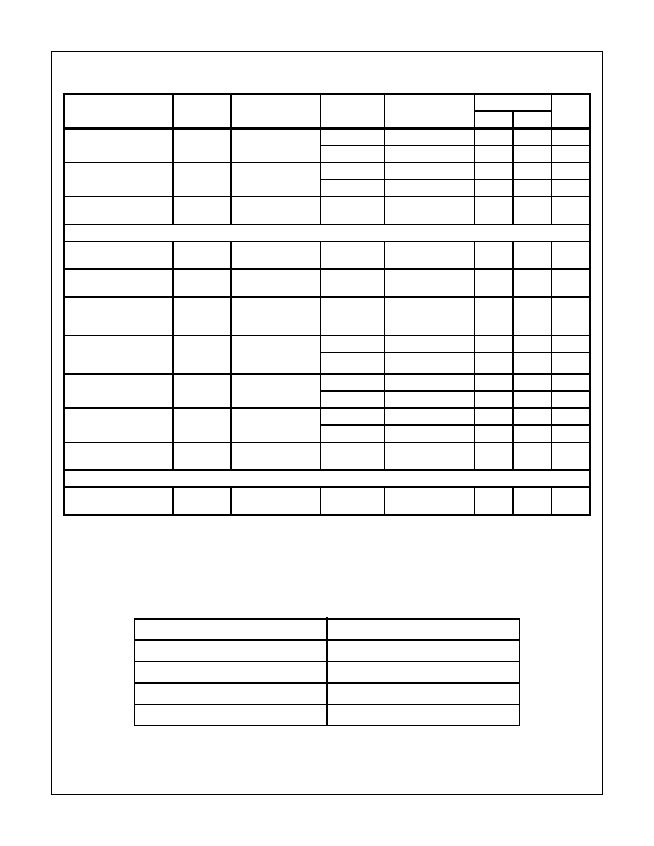
TABLE 2. AC ELECTRICAL PERFORMANCE CHARACTERISTICS
Table 2 Intentionally Left Blank. See AC Specifications in Table 3.
TABLE 3. ELECTRICAL PERFORMANCE CHARACTERISTICS
Device Tested: at V
SUPPLY
=
±
15V, R
F
= 50
, R
L
= 1k
, C
L
= 20pF, Unless Otherwise Specified.
PARAMETERS
SYMBOL
CONDITIONS
NOTES
TEMPERATURE
LIMITS
UNITS
MIN
MAX
V
Y
, V
Z
CHARACTERISTICS (NOTE 2)
Bandwidth
BW(V
Y
)
-3dB, V
X
= 5V,
V
Y
200mV
P-P
1
+25
o
C
30
-
MHz
Gain Flatness
GF(V
Y
)
0.1dB, V
X
= 5V,
V
Y
200mV
P-P
1
+25
o
C
4.0
-
MHz
AC Feedthrough
V
ISO
f
O
= 5MHz,
V
Y
= 200mV
P-P
V
X
= Nulled
1, 3
+25
o
C
-
-45
dB
Rise and Fall Time
T
R
, T
F
V
Y
= 200mV Step,
V
X
= 5V,
10% to 90% pts
1
+25
o
C
-
9.5
ns
1
+125
o
C, -55
o
C
-
10
ns
TABLE 1. DC ELECTRICAL PERFORMANCE CHARACTERISTICS
(Continued)
Device Tested at: V
SUPPLY
=
±
15V, R
F
= 50
, R
L
= 1k
, C
L
= 20pF, Unless Otherwise Specified.
PARAMETERS
SYMBOL
CONDITIONS
GROUP A
SUBGROUPS
TEMPERATURE
LIMITS
UNITS
MIN
MAX
Spec Number
511063-883
8-10
Specifications HA2556/883
Overshoot
+OS, -OS
V
Y
= 200mV step,
V
X
= 5V
1
+25
o
C
-
35
%
1
+125
o
C, -55
o
C
-
50
%
Slew Rate
+SR, -SR
V
Y
= 10V step,
V
X
= 5V
1
+25
o
C
410
-
V/
µ
s
1
+125
o
C, -55
o
C
360
-
V/
µ
s
Differential Input
Resistance
R
IN
(V
Y
)
V
Y
=
±
5V, V
X
= 0V
1
+25
o
C
650
-
k
V
X
CHARACTERISTICS
Bandwidth
BW (V
X
)
-3dB, V
Y
= 5V,
V
X
200mV
P-P
1
+25
o
C
30
-
MHz
Gain Flatness
GF (V
X
)
0.1dB, V
Y
= 5V,
V
X
200mV
P-P
1
+25
o
C
2.0
-
MHz
AC Feedthrough
V
ISO
f
O
= 5MHz,
V
X
= 200mV
P-P
V
Y
= Nulled
1, 3
+25
o
C
-
-45
dB
Rise & Fall Time
T
R
, T
F
V
X
= 200mV step,
V
Y
= 5V,
10% to 90% pts
1
+25
o
C
-
9.5
ns
1
+125
o
C, -55
o
C
-
10
ns
Overshoot
+OS, -OS
V
X
= 200mV step,
V
Y
= 5V
1
+25
o
C
-
35
%
1
+125
o
C, -55
o
C
-
50
%
Slew Rate
+SR, -SR
V
X
= 10V step,
V
Y
= 5V
1
+25
o
C
410
-
V/
µ
s
1
+125
o
C, -55
o
C
360
-
V/
µ
s
Differential Input
Resistance
R
IN
(V
X
)
V
X
=
±
5V, V
Y
= 0V
1
+25
o
C
650
-
k
OUTPUT CHARACTERISTICS
Output Resistance
R
OUT
V
Y
=
±
5V, V
X
= 5V
R
L
= 1k
to 250
1
+25
o
C
-
1
NOTES:
1. Parameters listed in Table 3 are controlled via design or process parameters and are not directly tested at final production. These param-
eters are lab characterized upon initial design release, or upon design changes. These parameters are guaranteed by characterization
based upon data from multiple production runs which reflect lot to lot and within lot variation.
2. V
Z
AC characteristics may be implied from V
Y
due to the use of V
Z
as feedback in the test circuit.
3. Offset voltage applied to minimize feedthrough signal.
TABLE 4. ELECTRICAL TEST REQUIREMENTS
MIL-STD-883 TEST REQUIREMENTS
SUBGROUPS (SEE TABLE 1)
Interim Electrical Parameters (Pre Burn-In)
-
Final Electrical Test Parameters
1 (Note 1), 2, 3
Group A Test Requirements
1, 2, 3
Groups C and D Endpoints
1
NOTE:
1. PDA applies to Subgroup 1 only. No other subgroups are included in PDA.
TABLE 3. ELECTRICAL PERFORMANCE CHARACTERISTICS
(Continued)
Device Tested: at V
SUPPLY
=
±
15V, R
F
= 50
, R
L
= 1k
, C
L
= 20pF, Unless Otherwise Specified.
PARAMETERS
SYMBOL
CONDITIONS
NOTES
TEMPERATURE
LIMITS
UNITS
MIN
MAX
Spec Number
511063-883
8-11
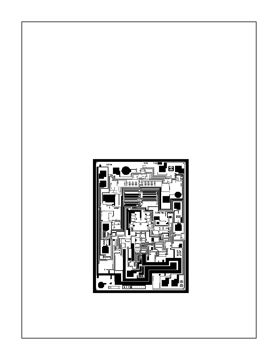
HA2556/883
Die Characteristics
DIE DIMENSIONS:
71mils x 100mils x 19mils
±
1mils
METALLIZATION:
Type: Al, 1% Cu
Thickness: 16k
≈
±
2k
≈
GLASSIVATION:
Type: Nitride (Si
3
N
4
) over Silox (SiO
2
, 5% Phos)
Silox Thickness: 12k
≈
±
2k
≈
Nitride Thickness: 3.5k
≈
±
1.5k
≈
TRANSISTOR COUNT: 84
SUBSTRATE POTENTIAL: V-
WORST CASE CURRENT DENSITY:
0.47 x 10
5
A/cm
2
Metallization Mask Layout
HA-2556/883
GND
(1)
V
REF
(2)
V
YIO
B (3)
V
YIO
A (4)
V
Y
+ (5)
V
Y
- (6)
V-
(7)
V
OUT
(8)
V
Z
+
(9)
V
Z
-
(10)
V+
(11)
V
X
-
(12)
V
X
+
(13)
V
XIO
B
(15)
V
XIO
A
(16)
Spec Number
511063-883
8-12
HA2556/883
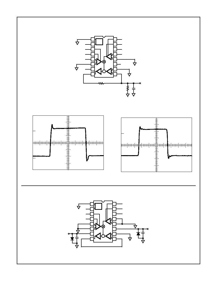
Test Waveforms
LARGE AND SMALL SIGNAL RESPONSE TEST CIRCUIT
LARGE SIGNAL RESPONSE
SMALL SIGNAL RESPONSE
2V/DIV; 100ns/DIV
50mV/DIV; 50ns/DIV
Burn-In Circuit
HA-2556/883 CERAMIC DIP
NC
NC
V
Y
+
-15V
V
OUT
+15 V
V
X
+
NC
NC
50
1K
20pF
NC
NC
V
Z
-
V
Z
+
14
15
16
9
13
12
11
10
1
2
3
4
5
7
6
8
+
-
REF
+
-
+
-
+
-
8
4
0
-4
-8
V
X
=
±
4V PULSE
V
Y
= 5V
DC
OUTPUT (V)
0ns
500ns
1
µ
s
0
OUTPUT (mV)
V
Y
=
±
100mV PULSE
V
X
= 5V
DC
0ns
250ns
500ns
200
100
-100
-200
-15.5V
0.01
µ
F
V
Z
-
V
Z
+
±
0.5V
D1
D1 = D2 = 1N4002 OR EQUIVALENT (PER BOARD)
NC
NC
V
Y
+
V
X
+
NC
NC
NC
NC
+15.5V
0.01
µ
F
±
0.5V
D2
V
OUT
14
15
16
9
13
12
11
10
1
2
3
4
5
7
6
8
+
-
REF
+
-
+
-
+
-
Spec Number
511063-883
8-13
HA2556/883
F16.3
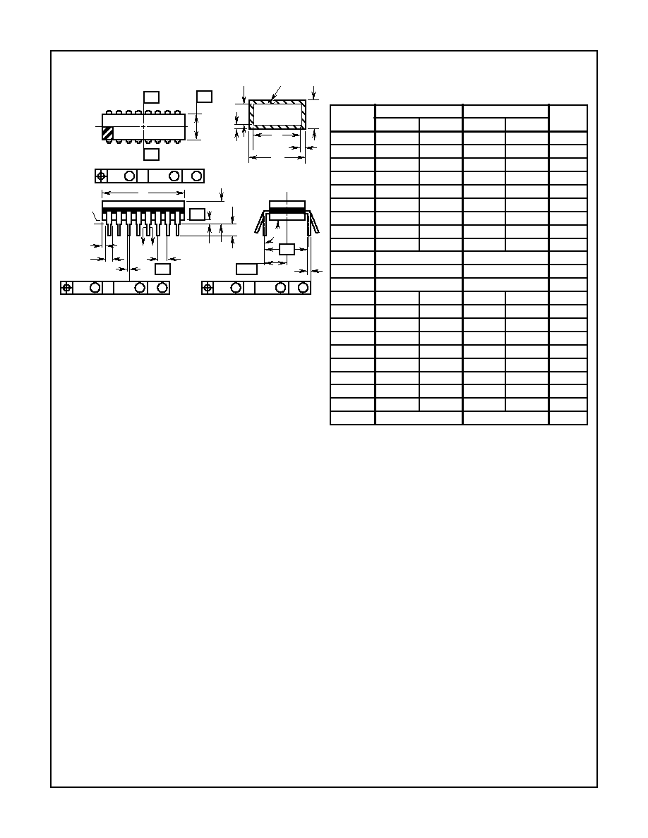
MIL-STD-1835 GDIP1-T16 (D-2, CONFIGURATION A)
16 LEAD DUAL-IN-LINE FRIT-SEAL CERAMIC PACKAGE
SYMBOL
INCHES
MILLIMETERS
NOTES
MIN
MAX
MIN
MAX
A
-
0.200
-
5.08
-
b
0.014
0.026
0.36
0.66
2
b1
0.014
0.023
0.36
0.58
3
b2
0.045
0.065
1.14
1.65
-
b3
0.023
0.045
0.58
1.14
4
c
0.008
0.018
0.20
0.46
2
c1
0.008
0.015
0.20
0.38
3
D
-
0.840
-
21.34
5
E
0.220
0.310
5.59
7.87
5
e
0.100 BSC
2.54 BSC
-
eA
0.300 BSC
7.62 BSC
-
eA/2
0.150 BSC
3.81 BSC
-
L
0.125
0.200
3.18
5.08
-
Q
0.015
0.060
0.38
1.52
6
S1
0.005
-
0.13
-
7
S2
0.005
-
0.13
-
-
90
o
105
o
90
o
105
o
-
aaa
-
0.015
-
0.38
-
bbb
-
0.030
-
0.76
-
ccc
-
0.010
-
0.25
-
M
-
0.0015
-
0.038
2
N
16
16
8
Packaging
NOTES:
1. Index area: A notch or a pin one identification mark shall be locat-
ed adjacent to pin one and shall be located within the shaded
area shown. The manufacturer's identification shall not be used
as a pin one identification mark.
2. The maximum limits of lead dimensions b and c or M shall be
measured at the centroid of the finished lead surfaces, when
solder dip or tin plate lead finish is applied.
3. Dimensions b1 and c1 apply to lead base metal only. Dimension
M applies to lead plating and finish thickness.
4. Corner leads (1, N, N/2, and N/2+1) may be configured with a
partial lead paddle. For this configuration dimension b3 replaces
dimension b1.
5. This dimension allows for off-center lid, meniscus, and glass overrun.
6. Dimension Q shall be measured from the seating plane to the
base plane.
7. Measure dimension S1 at all four corners.
8. N is the maximum number of terminal positions.
9. Dimensioning and tolerancing per ANSI Y14.5M - 1982.
10. Controlling Dimension: Inch.
11. Lead Finish: Type A.
12. Materials: Compliant to MIL-I-38535.
bbb
C A - B
S
c
Q
L
A
SEATING
BASE
D
PLANE
PLANE
-D-
-A-
-C-
-B-
D
E
S1
b2
b
A
e
M
c1
b1
(c)
(b)
SECTION A-A
BASE
LEAD FINISH
METAL
e
A/2
A
M
S
S
e
A
ccc
C A - B
M
D
S
S
aaa
C A - B
M
D
S
S
Spec Number
511063-883

The information contained in this section has been developed through characterization by Intersil Semiconductor and is for use as
application and design information only. No guarantee is implied.
8-14
DESIGN INFORMATION
August 1999
Semiconductor
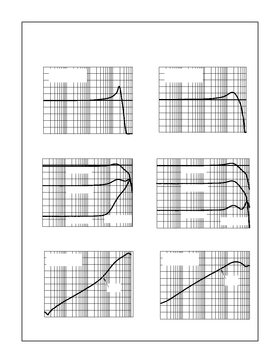
Typical Performance Curves
X CHANNEL MULTIPLIER ERROR
X CHANNEL MULTIPLIER ERROR
Y CHANNEL MULTIPLIER ERROR
Y CHANNEL MULTIPLIER ERROR
Y CHANNEL FULL POWER BANDWIDTH
Y CHANNEL FULL POWER BANDWIDTH
-6
-4
-2
0
2
4
6
-1
-0.5
0
0.5
1
X INPUT (V)
ERROR %FS
Y = 0
Y = 1
Y = 3
Y = 4
Y = 2
Y = 5
-6
-4
-2
0
2
4
6
-1.5
-1
-0.5
0
0.5
1
1.5
X INPUT (V)
ERROR %FS
Y = -4
Y = -2
Y = -1
Y = 0
Y = -5
Y = -3
-6
-4
-2
0
2
4
6
-1
-0.5
0
0.5
1
1.5
Y INPUT (V)
ERROR% FS
X = -3
X = -2
X = -4
X = -1
X = -5
X = 0
-6
-4
-2
0
2
4
6
-1.5
-1
-0.5
0
0.5
1
Y INPUT (V)
ERROR%FS
X = 0
X = 5
X = 1
X = 2
X = 4
X = 3
2
0
-2
GAIN (dB)
-1
-3
3
4
1
-4
1M
10M
100K
10K
Y CHANNEL = 10V
P-P
X CHANNEL = 5V
DC
FREQUENCY (Hz)
-3dB
AT 32.5MHz
1M
10M
100K
10K
FREQUENCY (Hz)
2
0
-2
GAIN (dB)
-1
-3
3
4
1
-4
Y CHANNEL = 4V
P-P
X CHANNEL = 5V
DC
HA2556
Wideband Four Quadrant
Analog Multiplier
Spec Number
511063-883
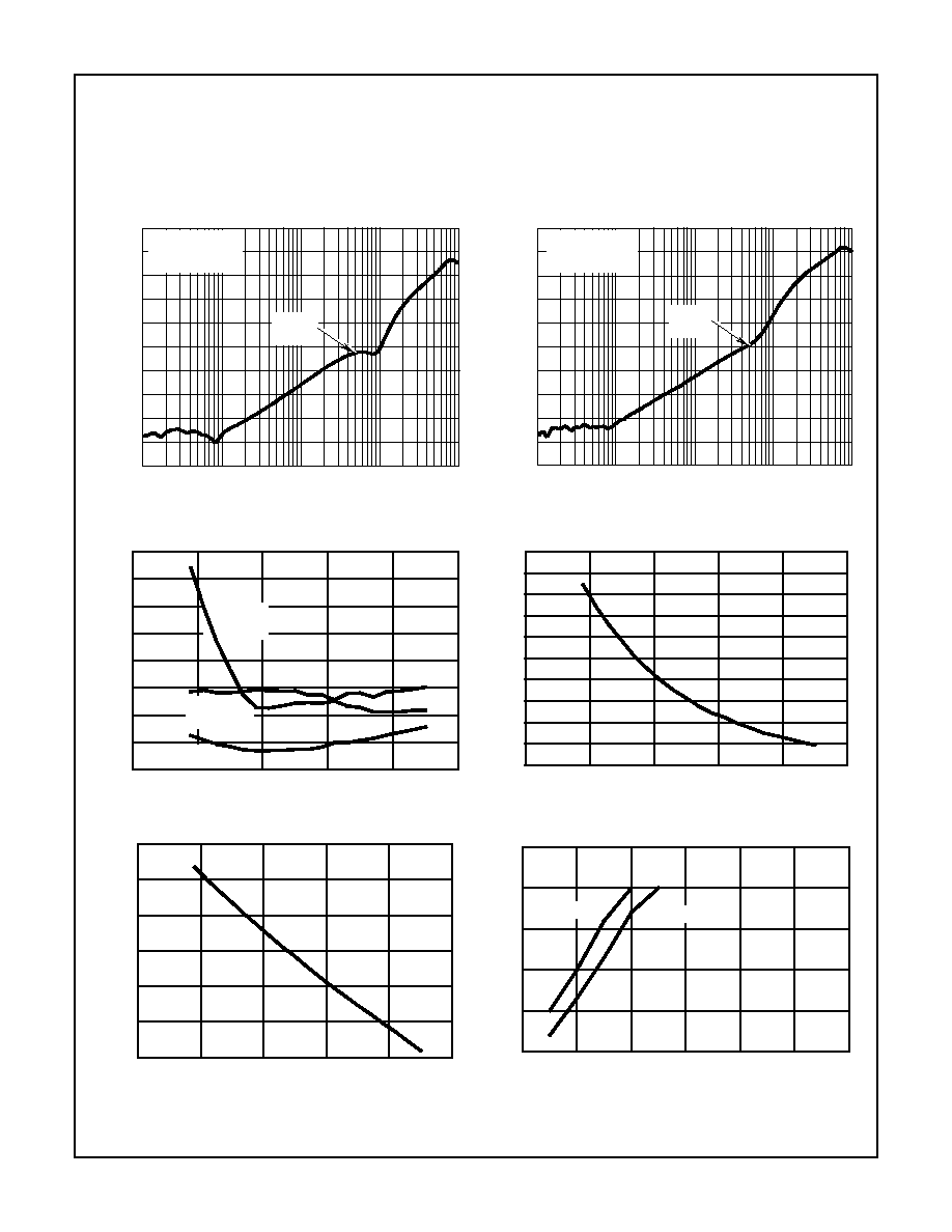
DESIGN INFORMATION
(Continued)
The information contained in this section has been developed through characterization by Intersil Semiconductor and is for use as
application and design information only. No guarantee is implied.
8-15
HA2556
X CHANNEL FULL POWER BANDWIDTH
X CHANNEL FULL POWER BANDWIDTH
Y CHANNEL BANDWIDTH vs X CHANNEL
X CHANNEL BANDWIDTH vs Y CHANNEL
Y CHANNEL CMRR vs FREQUENCY
X CHANNEL CMRR vs FREQUENCY
Typical Performance Curves
(Continued)
1M
10M
100K
10K
FREQUENCY (Hz)
2
0
-2
GAIN (dB)
-1
-3
3
4
1
-4
X CHANNEL = 10V
P-P
Y CHANNEL = 5V
DC
X CHANNEL = 4V
P-P
Y CHANNEL = 5V
DC
2
0
-2
GAIN (dB)
-1
-3
3
4
1
-4
1M
10M
100K
10K
FREQUENCY (Hz)
10M
100M
1M
FREQUENCY (Hz)
10K
100K
0
-12
GAIN (dB)
-6
-18
-24
V
X
= 0.5V
DC
V
X
= 2V
DC
V
X
= 5V
DC
V
Y
= 200mV
P-P
0
-12
GAIN (dB)
-6
-18
-24
10M
100M
1M
FREQUENCY (Hz)
10K
100K
V
X
= 200mV
P-P
V
Y
= 0.5V
DC
V
Y
= 2V
DC
V
Y
= 5V
DC
1M
100M
100K
10K
FREQUENCY (Hz)
-30
-50
-70
CMRR (dB)
-60
-80
-20
-10
-40
10M
5MHz
-38.8dB
0
V
Y
+, V
Y
- = 200mV
RMS
V
X
= 5V
DC
5MHz
-26.2dB
-30
-50
-70
CMRR (dB)
-60
-80
-20
-10
-40
0
1M
100M
100K
10K
FREQUENCY (Hz)
10M
V
X
+, V
X
- = 200mV
RMS
V
Y
= 5V
DC
Spec Number
511063-883
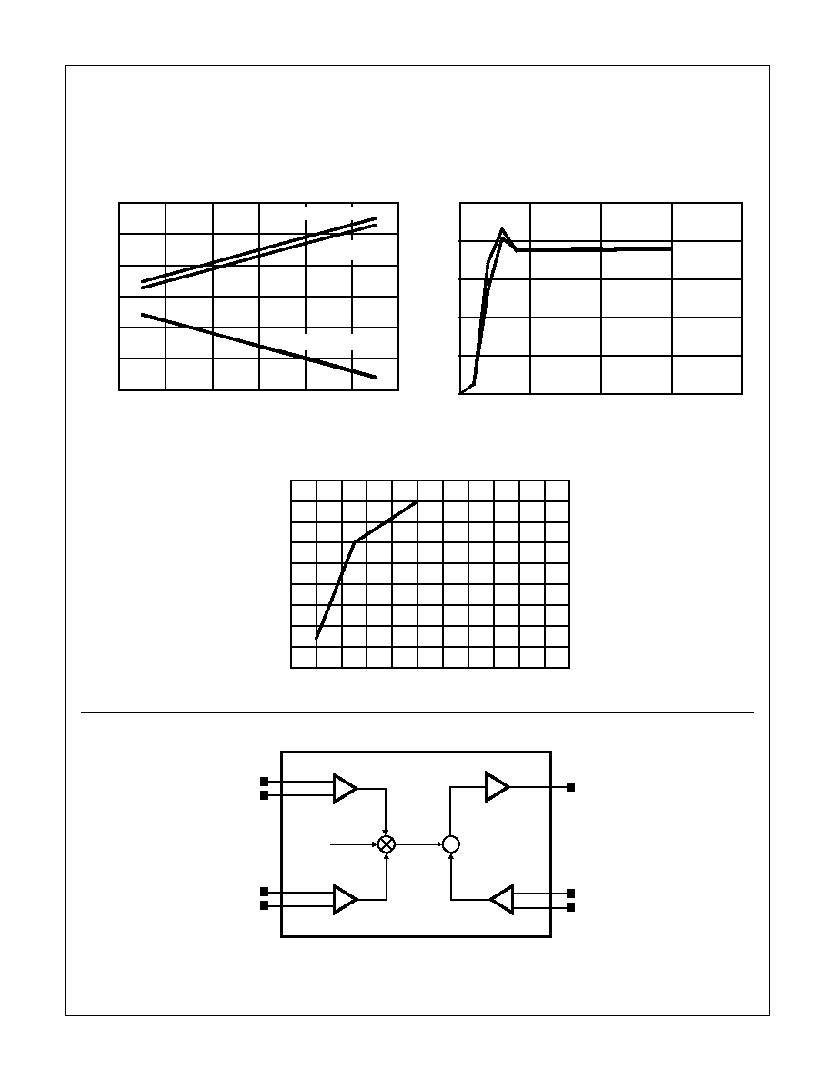
DESIGN INFORMATION
(Continued)
The information contained in this section has been developed through characterization by Intersil Semiconductor and is for use as
application and design information only. No guarantee is implied.
8-16
HA2556
FEEDTHROUGH vs FREQUENCY
FEEDTRHOUGH vs FREQUENCY
OFFSET VOLTAGE vs TEMPERATURE
INPUT BIAS CURRENT (V
X
, V
Y
, V
Z
) vs TEMPERATURE
SCALE FACTOR ERROR vs TEMPERATURE
INPUT VOLTAGE RANGE vs SUPPLY VOLTAGE
Typical Performance Curves
(Continued)
1M
100M
100K
10K
FREQUENCY (Hz)
10M
-52.6dB
at 5MHz
-30
-50
-70
FEEDTHROUGH (dB)
-60
-80
-20
-10
-40
0
V
X
= 200mV
P-P
V
Y
= NULLED
V
Y
= 200mV
P-P
V
X
= NULLED
-49dB
at 5MHz
-30
-50
-70
FEEDTHROUGH (dB)
-60
-80
-20
-10
-40
0
1M
100M
100K
10K
FREQUENCY (Hz)
10M
-100
-50
0
50
100
150
0
1
2
3
4
5
6
7
8
TEMPERATURE (
o
C)
OFFSET
VOL
T
AGE
(
m
V)
|V
IO
Z|
|V
IO
X|
|V
IO
Y|
-100
-50
0
50
100
150
4
5
6
7
8
9
10
11
12
13
14
TEMPERATURE (
o
C)
BIAS CURRENT (uA)
-100
-50
0
50
100
150
-1
-0.5
0
0.5
1
1.5
2
TEMPERATURE (
o
C)
SCALE F
ACT
OR ERROR (%)
4
6
8
10
12
14
16
1
2
3
4
5
6
±
SUPPLY VOLTAGE (V)
INPUT VOL
T
AGE RANGE (V)
X INPUT
Y INPUT
Spec Number
511063-883
DESIGN INFORMATION
(Continued)
The information contained in this section has been developed through characterization by Intersil Semiconductor and is for use as
application and design information only. No guarantee is implied.
8-17
HA2556
INPUT COMMON MODE RANGE vs SUPPLY VOLTAGE
SUPPLY CURRENT vs SUPPLY VOLTAGE
OUTPUT VOLTAGE vs R
LOAD
Functional Block Diagram
NOTE:
The transfer equation for the HA-2556 is:
(V
X
+ - V
X
-) (V
Y
+ - V
Y
-) = SF (V
Z
+ - V
Z
-),
where SF = Scale Factor = 5V V
X
, V
Y
, V
Z
= Differential Inputs
Typical Performance Curves
(Continued)
4
6
8
10
12
14
16
-15
-10
-5
0
5
10
15
±
SUPPLY VOLTAGE (V)
CMR (V)
X & Y INPUT
X INPUT
Y INPUT
0
5
10
15
20
0
5
10
15
20
25
±
SUPPLY VOLTAGE (V)
SUPPL
Y CURRENT (mA)
I
EE
I
CC
100
300
500
700
900
1100
4.2
4.4
4.6
4.8
5.0
R
LOAD
(
)
MAX OUTPUT VOL
T
AGE (V)
HA-2556
1/SF
X
Y
V
OUT
Z
V
X
+
V
X
-
V
Y
+
V
Y
-
V
Z
+
V
Z
-
+
-
A
+
-
+
-
+
-
Spec Number
511063-883

DESIGN INFORMATION
(Continued)
The information contained in this section has been developed through characterization by Intersil Semiconductor and is for use as
application and design information only. No guarantee is implied.
8-18
HA2556
Applications Information
Operation at Reduced Supply Voltages
The HA-2556 will operate over a range of supply voltages,
±
5V to
±
15V. Use of supply voltages below
±
12V will reduce
input and output voltage ranges. See "Typical Performance
Curves" for more information.
Offset Adjustment
X and Y channel offset voltages may be nulled by using a
20K potentiometer between the V
YIO
or V
XIO
adjust pin A
and B and connecting the wiper to V-. Reducing the channel
offset voltage will reduce AC feedthrough and improve the
multiplication error. Output offset voltage can also be nulled
by connecting V
Z
- to the wiper of a potentiometer which is
tied between V+ and V-.
Capacitive Drive Capability
When driving capacitive loads >20pF a 50
resistor should
be connected between V
OUT
and V
Z
+, using V
Z
+ as the out-
put (see Figure 1). This will prevent the multiplier from going
unstable and reduce gain peaking at high frequencies. The
50
resistor will dampen the resonance formed with the
capacitive load and the inductance of the output at pin 8.
Gain accuracy will be maintained because the resistor is
inside the feedback loop.
Theory of Operation
The HA-2556 creates an output voltage that is the product of
the X and Y input voltages divided by a constant scale factor
of 5V. The resulting output has the correct polarity in each of
the four quadrants defined by the combinations of positive
and negative X and Y inputs. The Z stage provides the
means for negative feedback (in the multiplier configuration)
and an input for summation into the output. This results in
the following equation, where X, Y and Z are high imped-
ance differential inputs
.
FIGURE 1. DRIVING CAPACITIVE LOAD
NC
NC
V
Y
+
-15V
V
OUT
+15 V
V
X
+
NC
NC
50
1K
20pF
NC
NC
V
Z
-
V
Z
+
14
15
16
9
13
12
11
10
1
2
3
4
5
7
6
8
+
-
REF
+
-
+
-
+
-
V
OUT
X x Y
5
----------
Z
≠
=
To accomplish this the differential input voltages are first con-
verted into differential currents by the X and Y input transcon-
ductance stages. The currents are then scaled by a constant
reference and combined in the multiplier core. The multiplier
core is a basic Gilbert Cell that produces a differential output
current proportional to the product of X and Y input signal cur-
rents. This current becomes the output for the HA-2557.
The HA-2556 takes the output current of the core and feeds
it to a transimpedance amplifier, that converts the current to
a voltage. In the multiplier configuration, negative feedback
is provided with the Z transconductance amplifier by con-
necting V
OUT
to the Z input. The Z stage converts V
OUT
to a
current which is subtracted from the multiplier core before
being applied to the high gain transimpedance amp. The Z
stage, by virtue of it's similarity to the X and Y stages, also
cancels second order errors introduced by the dependence
of V
BE
on collector current in the X and Y stages.
The purpose of the reference circuit is to provide a stable
current, used in setting the scale factor to 5V. This is
achieved with a bandgap reference circuit to produce a tem-
perature stable voltage of 1.2V which is forced across a NiCr
resistor. Slight adjustments to scale factor may be possible
by overriding the internal reference with the V
REF
pin. The
scale factor is used to maintain the output of the multiplier
within the normal operating range of
±
5V when full scale
inputs are applied.
The Balance Concept
The open loop transfer equation for the HA-2556 is:
where;
A = Output Amplifier Open Loop Gain
V
X
, V
Y
, V
Z
= Differential Input Voltages
5V = Fixed Scale Factor
An understanding of the transfer function can be gained by
assuming that the open loop gain, A, of the output amplifier
is infinite. With this assumption, any value of V
OUT
can be
generated with an infinitesimally small value for the terms
within the brackets. Therefore we can write the equation:
which simplifies to:
This form of the transfer equation provides a useful tool to
analyze multiplier application circuits and will be called the
Balance Concept.
V
OUT
A
V
X+
V
X-
≠
V
Y+
V
Y-
≠
◊
5
---------------------------------------------------------------------------
V
Z+
V
Z-
≠
≠
=
0
V
X+
V
X-
≠
(
)
V
Y+
V
Y-
≠
(
)
◊
5
-----------------------------------------------------------------
V
Z+
V
Z-
≠
(
)
≠
=
V
X+
V
X-
≠
(
)
V
Y+
V
Y-
≠
(
)
◊
5 V
Z+
V
Z-
≠
(
)
=
Spec Number
511063-883

DESIGN INFORMATION
(Continued)
The information contained in this section has been developed through characterization by Intersil Semiconductor and is for use as
application and design information only. No guarantee is implied.
8-19
HA2556
Let's first examine the Balance Concept as it applies to the
standard multiplier configuration (Figure 2).
Signals A and B are input to the multiplier and the signal W
is the result. By substituting the signal values into the Bal-
ance equation you get:
And solving for W:
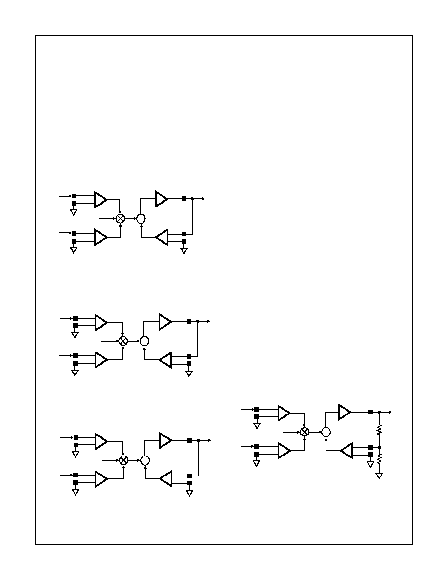
FIGURE 2. MULTIPLIER
Notice that the output (W) enters the equation in the feed-
back to the Z stage. The Balance Equation does not test for
stability, so remember that you must provide negative feed-
back. In the multiplier configuration, the feedback path is
connected to V
Z
+ input, not V
Z
-. This is due to the inversion
that takes place at the summing node just prior to the output
amplifier. Feedback is not restricted to the Z stage, other
feedback paths are possible as in the Divider Configuration
shown in Figure 3.
FIGURE 3. DIVIDER
Inserting the signal values A, B and W into the Balance
Equation for the divider configuration yields:
Solving for W yields:
Notice that, in the divider configuration, signal B must remain
0 (positive) for the feedback to be negative. If signal B is
negative, then it will be multiplied by the V
X-
input to produce
positive feedback and the output will swing into the rail.
A
( )
B
( )
◊
5 W
( )
=
W
A
B
◊
5
------------
=
HA-2556
1/5V
X
Y
V
OUT
Z
V
X
+
V
X
-
V
Y
+
V
Y
-
V
Z
+
V
Z
-
W
A
B
+
-
+
-
A
+
-
+
-
HA-2556
1/5V
X
Y
V
OUT
Z
V
X
+
V
X
-
V
Y
+
V
Y
-
V
Z
+
V
Z
-
W
A
B
+
-
+
-
+
-
A
+
-
W
≠
(
)
B
( )
◊
5V
A
≠
( )
◊
=
W
5A
B
-----
=
Signals may be applied to more than one input at a time as
in the Squaring configuration in Figure 4:
Here the Balance equation will appear as:
FIGURE 4. SQUARE
Which simplifies to:
The last basic configuration is the Square Root as shown in
Figure 5. Here feedback is provided to both X and Y inputs.
FIGURE 5. SQUARE ROOT (FOR A > 0)
The Balance equation takes the form:
Which equates to:
Application Circuits
The four basic configurations (Multiply, Divide, Square and
Square Root) as well as variations of these basic circuits
have many uses.
Frequency Doubler
For example, if ACos(
) is substituted for signal A in the
Square function, then it becomes a Frequency Doubler and
the equation takes the form:
And using some trigonometric identities gives the result:
A
( )
A
( )
◊
5 W
( )
=
HA-2556
1/5V
X
Y
V
OUT
Z
V
X
+
V
X
-
V
Y
+
V
Y
-
V
Z
+
V
Z
-
W
A
A
+
-
+
-
+
-
+
-
W
A2
5
-----
=
HA-2556
1/5V
X
Y
V
OUT
Z
V
X
+
V
X
-
V
Y
+
V
Y
-
V
Z
+
V
Z
-
W
A
+
-
+
-
A
+
-
+
-
W
( )
W
≠
(
)
◊
5
A
≠
( )
=
W
5A
=
ACos
( )
(
)
ACos
( )
(
)
◊
5 W
( )
=
W
A2
10
-----
1
Cos 2
(
)
+
(
)
=
Spec Number
511063-883
DESIGN INFORMATION
(Continued)
The information contained in this section has been developed through characterization by Intersil Semiconductor and is for use as
application and design information only. No guarantee is implied.
8-20
HA2556
Square Root
The Square Root function can serve as a precision/wide
bandwidth compander for audio or video applications. A
compander improves the Signal to Noise Ratio for your sys-
tem by amplifying low level signals while attenuating or com-
pressing large signals (refer to Figure 17; X
0.5
curve). This
provides for better low level signal immunity to noise during
transmission. On the receiving end the original signal may
be reconstructed with the standard Square function.
FIGURE 6. AM SIGNAL GENERATION
FIGURE 7. SYNCHRONOUS AM DETECTION
FIGURE 8. PHASE DETECTION
HA-2556
1/5V
X
Y
V
OUT
Z
V
X
+
V
X
-
V
Y
+
V
Y
-
V
Z
+
V
Z
-
W
ACos(
)
CCos(
C
)
CARRIER
AUDIO
W
AC
10
------
Cos
C
A
≠
(
)
Cos
C
A
+
(
)
+
(
)
=
+
-
+
-
A
+
-
+
-
HA-2556
1/5V
X
Y
V
OUT
Z
V
X
+
V
X
-
V
Y
+
V
Y
-
V
Z
+
V
Z
-
W
AM SIGNAL
CARRIER
LIKE THE FREQUENCY DOUBLER YOU GET AUDIO CENTERED AT DC
AND 2F
C
.
+
-
+
-
A
+
-
+
-
HA-2556
1/5V
X
Y
V
OUT
Z
V
X
+
V
X
-
V
Y
+
V
Y
-
V
Z
+
V
Z
-
W
ACos(
)
ACos(
+
)
W
A2
10
-----
Cos
( )
Cos 2
+
(
)
+
(
)
=
DC COMPONENT IS PROPORTIONAL TO Cos(f).
+
-
+
-
A
+
-
+
-
Communications
The Multiplier configuration has applications in AM Signal Gener-
ation, Synchronous AM Detection and Phase Detection to men-
tion a few. These circuit configurations are shown in Figure 6,
Figure 7 and Figure 8. The HA-2556 is particularly useful in
applications that require high speed signals on all inputs.
Each input X, Y and Z has similar wide bandwidth and input
characteristics. This is unlike earlier products where one
input was dedicated to a slow moving control function as is
required for Automatic Gain Control. The HA-2556 is versa-
tile enough for both.
Although the X and Y inputs have similar AC characteristics, they
are not the same. The designer should consider input parame-
ters such as small signal bandwidth, ac feedthrough and 0.1dB
gain flatness to get the most performance from the HA-2556.
The Y channel is the faster of the two inputs with a small signal
bandwidth of typically 57MHz verses 52MHz for the X channel.
Therefore in AM Signal Generation, the best performance will be
obtained with the Carrier applied to the Y channel and the modu-
lation signal (lower frequency) applied to the X channel.
Scale Factor Control
The HA-2556 is able to operate over a wide supply voltage range
±
5V to
±
17.5V. The
±
5V range is particularly useful in video appli-
cations. At
±
5V the input voltage range is reduced to
±
1.4V. The
output cannot reach its full scale value with this restricted input,
so it may become necessary to modify the scale factor. Adjusting
the scale factor may also be useful when the input signal itself is
restricted to a small portion of the full scale level. Here we can
make use of the high gain output amplifier by adding external
gain resistors. Generating the maximum output possible for a
given input signal will improve the Signal to Noise Ratio and
Dynamic Range of the system. For example, let's assume that
the input signals are 1V
PEAK
each. Then the maximum output for
the HA-2556 will be 200mV. (1V x 1V / (5V) = 200mV. It would be
nice to have the output at the same full scale as our input, so let's
add a gain of 5 as shown in Figure 9.
FIGURE 9. EXTERNAL GAIN OF 5
One caveat is that the output bandwidth will also drop by this
factor of 5. The multiplier equation then becomes:
HA-2556
1/5V
X
Y
V
OUT
Z
V
X
+
V
X
-
V
Y
+
V
Y
-
V
Z
+
V
Z
-
W
A
B
1k
250
R
F
R
G
ExternalGain
R
F
R
G
------
1
+
=
+
-
+
-
A
+
-
+
-
W
5AB
5
---------
A
B
◊
=
=
Spec Number
511063-883

DESIGN INFORMATION
(Continued)
The information contained in this section has been developed through characterization by Intersil Semiconductor and is for use as
application and design information only. No guarantee is implied.
8-21
HA2556
Current Output
Another useful circuit for low voltage applications allows the
user to convert the voltage output of the HA2556 to an out-
put current. The HA-2557 is a current output version offering
100MHz of bandwidth, but its scale factor is fixed and does
not have an output amplifier for additional scaling. Fortu-
nately the circuit in Figure 10 provides an output current that
can be scaled with the value of R
CONVERT
and provides an
output impedance of typically 1M
. The equation for I
OUT
becomes:
FIGURE 10. CURRENT OUTPUT
Video Fader
The Video Fader circuit provides a unique function. Here Ch
B is applied to the minus Z input in addition to the minus Y
input. In this way, the function in Figure 11 is generated. V
MIX
will control the percentage of Ch A and Ch B that are mixed
together to produce a resulting video image or other signal.
The Balance equation looks like:
Which simplifies to:
When V
MIX
is 0V the equation becomes V
OUT
= Ch B and
Ch A is removed, conversely when VMIX is 5V the equation
becomes V
OUT
= Ch A eliminating Ch B. For VMIX values 0V
VMIX
5V the output is a blend of Ch A and Ch B.
I
OUT
A
B
◊
5
------------
1
R
CONVERT
---------------------------
◊
=
HA-2556
1/5V
X
Y
V
OUT
Z
V
X
+
V
X
-
V
Y
+
V
Y
-
V
Z
+
V
Z
-
I
OUT
A
B
R
CONVERT
+
-
+
-
A
+
-
+
-
V
MIX
(
)
ChA
ChB
≠
(
)
◊
5 V
OUT
ChB
≠
(
)
=
V
OUT
ChB
V
MIX
5
-----------
ChA
ChB
≠
(
)
+
=
FIGURE 11. VIDEO FADER
FIGURE 12. DIFFERENCE OF SQUARES
FIGURE 13. PERCENTAGE DEVIATION
FIGURE 14. DIFFERENCE DIVIDED BY SUM (FOR A + B
0V)
NC
NC
V
Y
+
-15V
V
OUT
+15V
V
X
+
NC
NC
50
NC
NC
V
Z
-
V
Z
+
CH A
CH B
V
Y
-
V
MIX
(0V to 5V)
14
15
16
9
13
12
11
10
1
2
3
4
5
7
6
8
+
-
REF
+
-
+
-
+
-
HA-2556
1/5V
X
Y
Z
V
X
+
V
X
-
V
Y
+
V
Y
-
V
Z
+
V
Z
-
W = 5(A
2
-B
2
)
A
B
5K
5K
5K
5K
+
-
+
-
A
+
-
+
-
HA-2556
1/5V
X
Y
V
OUT
Z
V
X
+
V
X
-
V
Y
+
V
Y
-
V
Z
+
V
Z
-
W = 100
B
A
A - B
A
95K
5K
R2
R1
R1 and R2 set scale to 1V/%, other scale factors possible
for A
0V.
+
-
+
-
A
+
-
+
-
HA-2556
1/5V
X
Y
V
OUT
Z
V
X
+
V
X
-
V
Y
+
V
Y
-
V
Z
+
V
Z
-
W = 10
B
A
A - B
B + A
5K
5K
+
-
+
-
A
+
-
+
-
Spec Number
511063-883
DESIGN INFORMATION
(Continued)
The information contained in this section has been developed through characterization by Intersil Semiconductor and is for use as
application and design information only. No guarantee is implied.
8-22
HA2556
Other Applications
As shown above, a function may contain several different
operators at the same time and use only one HA-2556.
Some other possible multi-operator functions are shown in
Figure 12, Figure 13 and Figure 14.
Of course the HA-2556 is also well suited to standard multi-
plier applications such as Automatic Gain Control and Volt-
age Controlled Amplifier.
Automatic Gain Control
Figure 15 shows the HA-2556 configured in an Automatic
Gain Control or AGC application. The HA-5127 low noise
amplifier provides the gain control signal to the X input. This
control signal sets the peak output voltage of the multiplier to
match the preset reference level. The feedback network
around the HA-5127 provides a response time adjustment.
High frequency changes in the peak are rejected as noise or
the desired signal to be transmitted. These signals do not
indicate a change in the average peak value and therefore
no gain adjustment is needed. Lower frequency changes in
the peak value are given a gain of -1 for feedback to the
control input. At DC the circuit is an integrator automatically
compensating for Offset and other constant error terms.
This multiplier has the advantage over other AGC circuits, in
that the signal bandwidth is not affected by the control signal
gain adjustment.
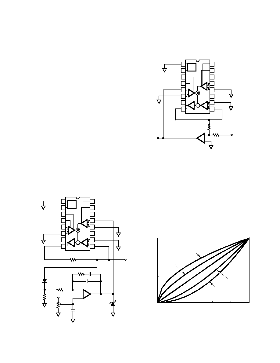
FIGURE 15. AUTOMATIC GAIN CONTROL
NC
NC
V
Y
+
-V
V
OUT
+V
NC
NC
50
HA-2556
5k
10k
HA-5127
0.01
µ
F
10k
0.1
µ
F
1N914
5.6V
0.1
µ
F
+15V
20k
NC
NC
+
-
14
15
16
9
13
12
11
10
1
2
3
4
5
7
6
8
+
-
REF
Y
X
Z
FIGURE 16. VOLTAGE CONTROLLED AMPLIFIER
Voltage Controlled Amplifier
A wide range of gain adjustment is available with the Voltage
Controlled Amplifier configuration shown in Figure 16. Here
the gain of the HFA0002 can be swept from 20V/V to a gain
of almost 1000V/V with a DC voltage from 0 to 5V.
Wave Shaping Circuits
Wave shaping or curve fitting is another class of application
for the analog multiplier. For example, where a non-linear
sensor requires corrective curve fitting to improve linearity
the HA-2556 can provide nonintegral powers in the range 1
to 2 or nonintegral roots in the range 0.5 to 1.0 (refer to Fur-
ther Reading). This effect is displayed in Figure 17.
FIGURE 17. EFFECT OF NONINTEGRAL POWERS / ROOTS
NC
NC
V
X
+ (V
GAIN
)
-V
V
IN
+ V
NC
NC
HFA0002
5k
V
OUT
500
NC
NC
HA-2556
+
-
14
15
16
9
13
12
11
10
1
2
3
4
5
7
6
8
+
-
REF
Y
X
Z
0
0.2
0.4
0.6
0.8
1
0
0.2
0.4
0.6
0.8
1
INPUT (V)
OUTPUT (V)
X
0.5
X
0.7
X
1.5
X
2
Spec Number
511063-883

DESIGN INFORMATION
(Continued)
The information contained in this section has been developed through characterization by Intersil Semiconductor and is for use as
application and design information only. No guarantee is implied.
8-23
HA2556
Well, OK a multiplier can't do nonintegral roots "exactly" but
we can get very close. We can approximate nonintegral
roots with equations of the form:
Figure 18 compares the function V
OUT
= V
IN
0.7
to the
approximation V
OUT
= 0.5V
IN
0.5
+ 0.5V
IN
.
FIGURE 18. COMPARE APPROXIMATION TO NONINTEGRAL
ROOT
This function can be easily built using an HA-2556 and a
potentiometer for easy adjustment as shown in Figures 19
and 20. If a fixed nonintegral power is desired, the circuit
shown in Figure 21 eliminates the need for the output buffer
amp. These circuits approximate the function V
IN
M
where M
is the desired nonintegral power or root.
FIGURE 19. NONINTEGRAL ROOTS - ADJUSTABLE
V
o
1
≠
(
)
V
IN
2
V
IN
+
=
V
o
1
≠
(
)
V
IN
1 2
/
V
IN
+
=
0
0.2
0.4
0.6
0.8
1
0
0.2
0.4
0.6
0.8
1
INPUT (V)
OUTPUT (V)
X
X
0.7
0.5X
0.5
+ 0.5X
NC
NC
-V
V
IN
+V
NC
NC
HA-2556
HA-5127
NC
NC
V
OUT
0V
V
IN
1V
0.5
M
1.0
1-
+
-
14
15
16
9
13
12
11
10
1
2
3
4
5
7
6
8
+
-
REF
Y
X
Z
+
-
+
-
+
-
FIGURE 20. NONINTEGRAL POWERS - ADJUSTABLE
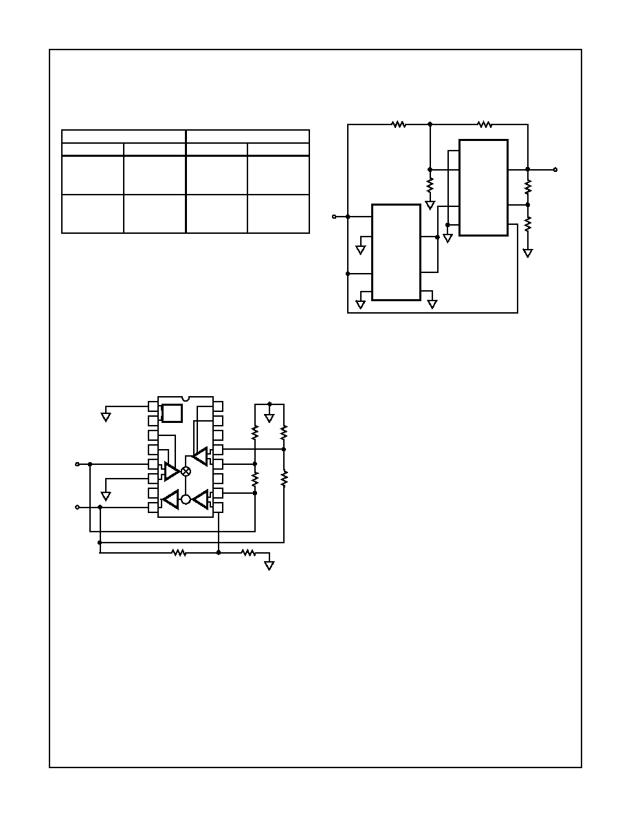
FIGURE 21. NONINTEGRAL POWERS - FIXED
NC
NC
-V
V
IN
+V
NC
NC
HA-2556
HA-5127
NC
NC
V
OUT
0V
V
IN
1V
1.0
M
2.0
1-
+
-
14
15
16
9
13
12
11
10
1
2
3
4
5
7
6
8
+
-
REF
Y
X
Z
+
-
+
-
+
-
NC
NC
-V
V
IN
+V
NC
NC
HA-2556
NC
NC
V
OUT
0V
V
IN
1V
1.2
M
2.0
R3
R4
R1
R2
V
OUT
1
5
--
R3
R4
-----
1
+
V
IN
2
R3
R4
-----
1
+
R2
R1
R2
+
-----------------
V
IN
+
=
1
≠
1
5
--
R3
R4
-----
1
+
=
R3
R4
-----
1
+
R2
R1
R2
+
-----------------
=
Setting:
14
15
16
9
13
12
11
10
1
2
3
4
5
7
6
8
+
-
REF
Y
X
Z
+
-
+
-
+
-
Spec Number
511063-883
DESIGN INFORMATION
(Continued)
The information contained in this section has been developed through characterization by Intersil Semiconductor and is for use as
application and design information only. No guarantee is implied.
8-24
HA2556
Values for
to give a desired M root or power are as follows:
Sine Function Generators
Similar functions can be formulated to approximate a SINE
function converter as shown in Figure 22. With a linearly
changing (0 to 5V) input the output will follow 0
o
to 90
o
of a
sine function (0 to 5V) output. This configuration is theoreti-
cally capable of
±
2.1% maximum error to full scale.
By adding a second HA-2556 to the circuit an improved fit
may be achieved with a theoretical maximum error of 0.5%
as shown in Figure 23. Figure 23 has the added benefit that
it will work for positive and negative input signals. This
makes a convenient triangle (
±
5V input) to sine wave (
±
5V
output) converter.
FIGURE 22. SINE-FUNCTION GENERATOR
ROOTS - FIGURE 19
POWERS - FIGURE 20
M
M
0.5
0
1.0
1
0.6
0.25
1.2
0.75
0.7
0.50
1.4
0.5
0.8
0.70
1.6
0.3
0.9
0.85
1.8
0.15
1.0
1
2.0
0
NC
NC
-V
V
IN
+V
NC
NC
HA-2556
NC
NC
V
OUT
R3
R4
V
OUT
V
IN
1
0.1284V
IN
≠
(
)
0.6082
0.05V
IN
≠
(
)
----------------------------------------
=
5sin
2
--
V
IN
5
-------
0.6082
R4
R3
R4
+
-----------------
=
5
0.1284
(
)
R2
R1
R2
+
-----------------
=
5
0.05
(
)
R6
R5
R6
+
-----------------
=
R2
R1
R6
R5
644
1K
262
470
470
1410
where:
;
for; 0V
VIN
5V
max theoretical error = 2.1%FS
14
15
16
9
13
12
11
10
1
2
3
4
5
7
6
8
+
-
REF
Y
X
Z
+
-
+
-
+
-
FIGURE 23. BIPOLAR SINE-FUNCTION GENERATOR
Further Reading
1. Pacifico Cofrancesco, "RF Mixers and ModulatorsMade
with a Monolithic Four-Quadrant Multiplier" Microwave
Journal, December 1991 pg. 58 - 70.
2. Richard Goller, "IC Generates Nonintegral Roots" Elec-
tronic Design, December 3, 1992.
V
OUT
5V
IN
0.05494V
IN
3
≠
3.18167
0.0177919V
IN
2
+
----------------------------------------------------
5
sin
2
--
V
IN
5
--------
=
10K
X
+
X
-
Y
+
Y
-
X
+
X
-
Y
+
Y
-
V
OUT
Z
+
Z
-
V
OUT
Z
+
Z
-
V
IN
V
OUT
HA-2556
HA-2556
23.1K
71.5K
5.71K
10K
-5V
V
IN
5V
max theoretical error = 0.5%FS
Spec Number
511063-883
DESIGN INFORMATION
(Continued)
The information contained in this section has been developed through characterization by Intersil Semiconductor and is for use as
application and design information only. No guarantee is implied.
8-25
HA2556
TYPICAL PERFORMANCE CHARACTERISTICS
Device Tested at Supply Voltage =
±
15V, R
F
= 50
, R
L
= 1k
, C
L
= 20pF, Unless Otherwise Specified.
PARAMETERS
SYMBOL
CONDITIONS
TEMP
TYP
UNITS
Multiplication Error
ME
V
Y
, V
X
=
±
5V
+25
o
C
±
1.5
%FS
+125
o
C, -55
o
C
±
3.0
%FS
Multiplication Error Drift
V
Y
, V
X
=
±
5V
+125
o
C, -55
o
C
±
0.003
%FS/
o
C
Linearity Error
LE3V
V
Y
, V
X
=
±
3V
+25
o
C
±
0.02
%FS
LE4V
V
Y
, V
X
=
±
4V
+25
o
C
±
0.05
%FS
LE5V
V
Y
, V
X
=
±
5V
+25
o
C
±
0.2
%FS
Differential Gain
DG
f = 4.43MHz, V
Y
= 300mV
P-P
, V
X
= 5V
+25
o
C
0.1
%
Differential Phase
DP
f = 4.43MHz, V
Y
= 300mV
P-P
, V
X
= 5V
+25
o
C
0.1
Deg.
Scale Factor
SF
+25
o
C
5
V
Voltage Noise
E
N
(1kHz)
f = 1kHz, V
X
= 0V, V
Y
= 0V
+25
o
C
150
nV/
Hz
E
N
(100kHz)
f = 100kHz, V
X
= 0V, V
Y
= 0V
+25
o
C
40
nV/
Hz
Positive Power Supply
Rejection Ratio
+PSRR
V
S
+ = +12V to +15V, V
S
- = -15V
+25
o
C
80
dB
+125
o
C, -55
o
C
80
dB
Negative Power Supply
Rejection Ratio
-PSRR
V
S
- = -12V to -15V, V
S
+ = +15V
+25
o
C
55
dB
+125
o
C, -55
o
C
55
dB
Supply Current
I
CC
V
X
, V
Y
= 0V
+25
o
C
18
mA
+125
o
C, -55
o
C
18
mA
INPUT CHARACTERISTICS
Input Offset Voltage
V
IO
V
Y
=
±
5V
+25
o
C
±
3
mV
+125
o
C, -55
o
C
±
8
mV
Input Offset Voltage Drift
V
IO
TC
V
Y
=
±
5V
+125
o
C, -55
o
C
±
45
µ
V/
o
C
Input Bias Current
I
B
V
X
= 0V, V
Y
= 5V
+25
o
C
±
8
µ
A
+125
o
C, -55
o
C
±
12
µ
A
Input Offset Current
I
IO
V
X
= 0V, V
Y
= 5V
+25
o
C
±
0.5
µ
A
+125
o
C, -55
o
C
±
1.0
µ
A
Differential Input Range
+25
o
C
±
5
V
Common Mode Range (V
X
)
CMR (V
X
)
+25
o
C
±
10
V
Common Mode Range (V
Y
)
CMR (V
Y
)
+25
o
C
+9, -10
V
Common Mode (V
X
)
Rejection Ratio
CMRR (V
X
)
V
X
CM =
±
10V, V
Y
= 5V
+25
o
C
78
dB
+125
o
C, -55
o
C
78
dB
Common Mode (V
Y
)
Rejection Ratio
CMRR (V
Y
)
V
Y
CM = +9V, -10V, V
X
= 5V
+25
o
C
78
dB
+125
o
C, -55
o
C
78
dB
Common Mode (V
Z
)
Rejection Ratio
CMRR (V
Z
)
V
Z
CM =
±
10V, V
X
= 0V, V
Y
= 0V
+25
o
C
78
dB
+125
o
C, -55
o
C
78
dB
V
Y
, V
Z
CHARACTERISTICS (Note 1)
Bandwidth
BW (V
Y
)
-3dB, V
X
= 5V, V
Y
200mV
P-P
+25
o
C
57
MHz
Gain Flatness
GF (V
Y
)
0.1dB, V
X
= 5V, V
Y
200mV
P-P
+25
o
C
5.0
MHz
AC Feedthrough
V
ISO
(1MHz)
f
O
= 1MHz, V
Y
= 200mV
P-P
, V
X
= nulled (Note 2)
+25
o
C
-65
dB
V
ISO
(5MHz)
f
O
= 5MHz, V
Y
= 200mV
P-P
, V
X
= nulled (Note 2)
+25
o
C
-50
dB
Rise and Fall Time
T
R
, T
F
V
Y
= 200mV step, V
X
= 5V, 10% to 90% pts
+25
o
C
8
ns
+125
o
C, -55
o
C
8
ns
Spec Number
511063-883

DESIGN INFORMATION
(Continued)
The information contained in this section has been developed through characterization by Intersil Semiconductor and is for use as
application and design information only. No guarantee is implied.
8-26
HA2556
Overshoot
+OS, -OS
V
Y
= 200mV step, V
X
= 5V
+25
o
C
17
%
+125
o
C, -55
o
C
17
%
Slew Rate
+SR, -SR
V
Y
= 10V step, V
X
= 5V
+25
o
C
450
V/
µ
s
+125
o
C, -55
o
C
450
V/
µ
s
Differential Input Resistance
R
IN
(V
Y
)
V
Y
=
±
5V, V
X
= 0V
+25
o
C
1
M
V
X
CHARACTERISTICS
Bandwidth
BW (V
X
)
-3dB, V
Y
= 5V, V
X
200mV
P-P
+25
o
C
52
MHz
Gain Flatness
GF (V
X
)
0.1dB, V
Y
= 5V, V
X
200mV
P-P
+25
o
C
4.0
MHz
AC Feedthrough
V
ISO
(1MHz)
f
O
= 1MHz, V
X
= 200mV
P-P
,V
Y
= nulled (Note 2)
+25
o
C
-65
dB
V
ISO
(5MHz)
f
O
= 5MHz, V
X
= 200mV
P-P
, V
Y
= nulled (Note 2)
+25
o
C
-50
dB
Rise & Fall Time
T
R
, T
F
V
X
= 200mV step, V
Y
= 5V, 10% to 90% pts
+25
o
C
8
ns
+125
o
C, -55
o
C
8
ns
Overshoot
+OS, -OS
V
X
= 200mV step, V
Y
= 5V
+25
o
C
17
%
+125
o
C, -55
o
C
17
%
Slew Rate
+SR, -SR
V
X
= 10V step, V
Y
= 5V
+25
o
C
450
V/
µ
s
+125
o
C, -55
o
C
450
V/
µ
s
Differential Input Resistance
R
IN
(V
X
)
V
X
=
±
5V, V
Y
= 0V
+25
o
C
1
M
OUTPUT CHARACTERISTICS
Output Resistance
R
OUT
V
Y
=
±
5V, V
X
= 5V, R
L
= 1k
to 250
+25
o
C
0.7
Output Current
I
OUT
V
OUT
= 5V, R
L
= 250
+25
o
C
±
45
mA
+125
o
C, -55
o
C
±
45
mA
Output Voltage Swing
+V
OUT
R
L
= 250
+25
o
C
±
6.05
V
+125
o
C, -55
o
C
±
6.05
V
NOTES:
1. V
Z
AC characteristics may be implied from V
Y
due to the use of V
Z
as feedback in the test circuit.
2. Offset voltage applied to minimize feedthrough signal.
TYPICAL PERFORMANCE CHARACTERISTICS
(Continued)
Device Tested at Supply Voltage =
±
15V, R
F
= 50
, R
L
= 1k
, C
L
= 20pF, Unless Otherwise Specified.
PARAMETERS
SYMBOL
CONDITIONS
TEMP
TYP
UNITS
Spec Number
511063-883
All Intersil semiconductor products are manufactured, assembled and tested under ISO9000 quality systems certification.
Intersil products are sold by description only. Intersil Corporation reserves the right to make changes in circuit design and/or specifications at any time without
notice. Accordingly, the reader is cautioned to verify that data sheets are current before placing orders. Information furnished by Intersil is believed to be accurate
and reliable. However, no responsibility is assumed by Intersil or its subsidiaries for its use; nor for any infringements of patents or other rights of third parties which
may result from its use. No license is granted by implication or otherwise under any patent or patent rights of Intersil or its subsidiaries.
For information regarding Intersil Corporation and its products, see web site http://www.intersil.com