
3-230
CAUTION: These devices are sensitive to electrostatic discharge; follow proper IC Handling Procedures.
http://www.intersil.com or 407-727-9207
|
Copyright
©
Intersil Corporation 1999
HA-2842/883
Wideband, High Slew Rate, High Output Current,
Video Operational Amplifier
Description
The HA-2842/883 is a wideband, high slew rate, operational
amplifier featuring an outstanding combination of speed,
bandwidth, and output drive capability. This amplifier's per-
formance is further enhanced through stable operation down
to closed loop gains of +2, the inclusion of offset null con-
trols, and by its excellent video performance.
The capabilities of the HA-2842/883 are ideally suited for
high speed cable driver circuits, where low closed loop gains
and high output drive are required. With a 6MHz full power
bandwidth, this amplifier is well suited for high frequency sig-
nal conditioning circuits and video amplifiers. Gain flatness
of 0.035dB, combined with differential gain and phase speci-
fications of 0.02%, and 0.03 degrees, respectively, make the
HA-2842/883 ideal for component and composite video
applications.
A zener/nichrome based reference circuit, coupled with
advanced laser trimming techniques, yields a supply current
with a low temperature coefficient and low lot-to-lot variabil-
ity. For example, the average I
CC
variation from +85
o
C to
-40
o
C is <600
µ
A (
±
2%),while the standard deviation of the
I
CC
distribution is <0.1mA (0.8%) at +25
o
C. Tighter I
CC
con-
trol translates to more consistent AC parameters ensuring
that units from each lot perform the same way, and easing
the task of designing systems for wide temperature ranges.
Ordering Information
PART
NUMBER
TEMPERATURE
RANGE
PACKAGE
HA1-2842/883
-55
o
C to +125
o
C
14 Lead CerDIP
HA7-2842/883
-55
o
C to +125
o
C
8 Lead CerDIP
Features
∑ This Circuit is Processed in Accordance to MIL-STD-
883 and is Fully Conformant Under the Provisions of
Paragraph 1.2.1.
∑ Low AC Variability Over Process and Temperature
∑ Stable at Gains of 2 or Greater
∑ Low Supply Current . . . . . . . . . . . . . . . . . . 15mA (Max)
∑ Gain Bandwidth Product . . . . . . . . . . . . . . 80MHz (Typ)
∑ High Slew Rate . . . . . . . . . . . . . . . . . . . . . 375V/
µ
s (Typ)
∑ High Output Current . . . . . . . . . . . . . . . . . 100mA (Min)
∑ Full Power Bandwidth . . . . . . . . . . . . . . . . . 6MHz (Typ)
∑ Low Differential Gain/Phase . . . . . . . 0.02%/0.03
o
(Typ)
Applications
∑ Coaxial Cable Drivers
∑ Pulse and Video Amplifiers
∑ Wideband Amplifiers
∑ Fast Sample and Hold Circuits
∑ High Frequency Signal Conditioning Circuits
July 1994
Pinouts
HA-2842/883
(CERDIP)
TOP VIEW
HA-2842/883
(CERDIP)
TOP VIEW
NOTE: (NC) No Connection pins may be tied to a ground plane for better isolation and heat dissipation.
NC
NC
BAL
-IN
+IN
V-
NC
NC
BAL
NC
V+
OUT
NC
NC
1
2
3
4
5
6
7
14
13
12
11
10
9
8
-
+
BAL
-IN
+IN
V-
1
2
3
4
8
7
6
5
BAL
V+
OUT
NC
-
+
Spec Number
511088-883
File Number
3622.1
3-231
Specifications HA-2842/883
Absolute Maximum Ratings
Thermal Information
Voltage between V+ and V- Terminals . . . . . . . . . . . . . . . . . . . . 35V
Differential Input Voltage . . . . . . . . . . . . . . . . . . . . . . . . . . . . . . . 6V
Voltage at Either Input Terminal . . . . . . . . . . . . . . . . . . . . . . V+ to V-
Peak Output Current (
40% Duty Cycle) . . . . . . . . . . . . . . . . 125mA
Junction Temperature (T
J
) (Note 1) . . . . . . . . . . . . . . . . . . . +175
o
C
Storage Temperature Range . . . . . . . . . . . . . . . . . -65
o
C to +150
o
C
ESD Rating. . . . . . . . . . . . . . . . . . . . . . . . . . . . . . . . . . . . . . <2000V
Lead Temperature (Soldering 10s). . . . . . . . . . . . . . . . . . . . +300
o
C
Thermal Resistance
JA
JC
14 Lead CerDIP Package . . . . . . . . . . . .
73
o
C/W
18
o
C/W
8 Lead CerDIP Package . . . . . . . . . . . . .
110
o
C/W
27
o
C/W
Package Power Dissipation Limit at +75
o
C for T
J
+175
o
C
14 Lead CerDIP Package . . . . . . . . . . . . . . . . . . . . . . . . . . . 1.1W
8 Lead CerDIP Package . . . . . . . . . . . . . . . . . . . . . . . . . . . . 0.9W
Package Power Dissipation Derating Factor Above +75
o
C
14 Lead CerDIP Package . . . . . . . . . . . . . . . . . . . . . . . 11mW/
o
C
8 Lead CerDIP Package . . . . . . . . . . . . . . . . . . . . . . . . . 9mW/
o
C
CAUTION: Stresses above those listed in "Absolute Maximum Ratings" may cause permanent damage to the device. This is a stress only rating and operation
of the device at these or any other conditions above those indicated in the operational sections of this specification is not implied.
Operating Conditions
Operating Temperature Range. . . . . . . . . . . . . . . . -55
o
C to +125
o
C
Operating Supply Voltage
. . . . . . . . . . . . . . . . . . . . . . . . . ±
12V to
±
15V
V
INCM
1/2(V+ - V-)
R
L
1k
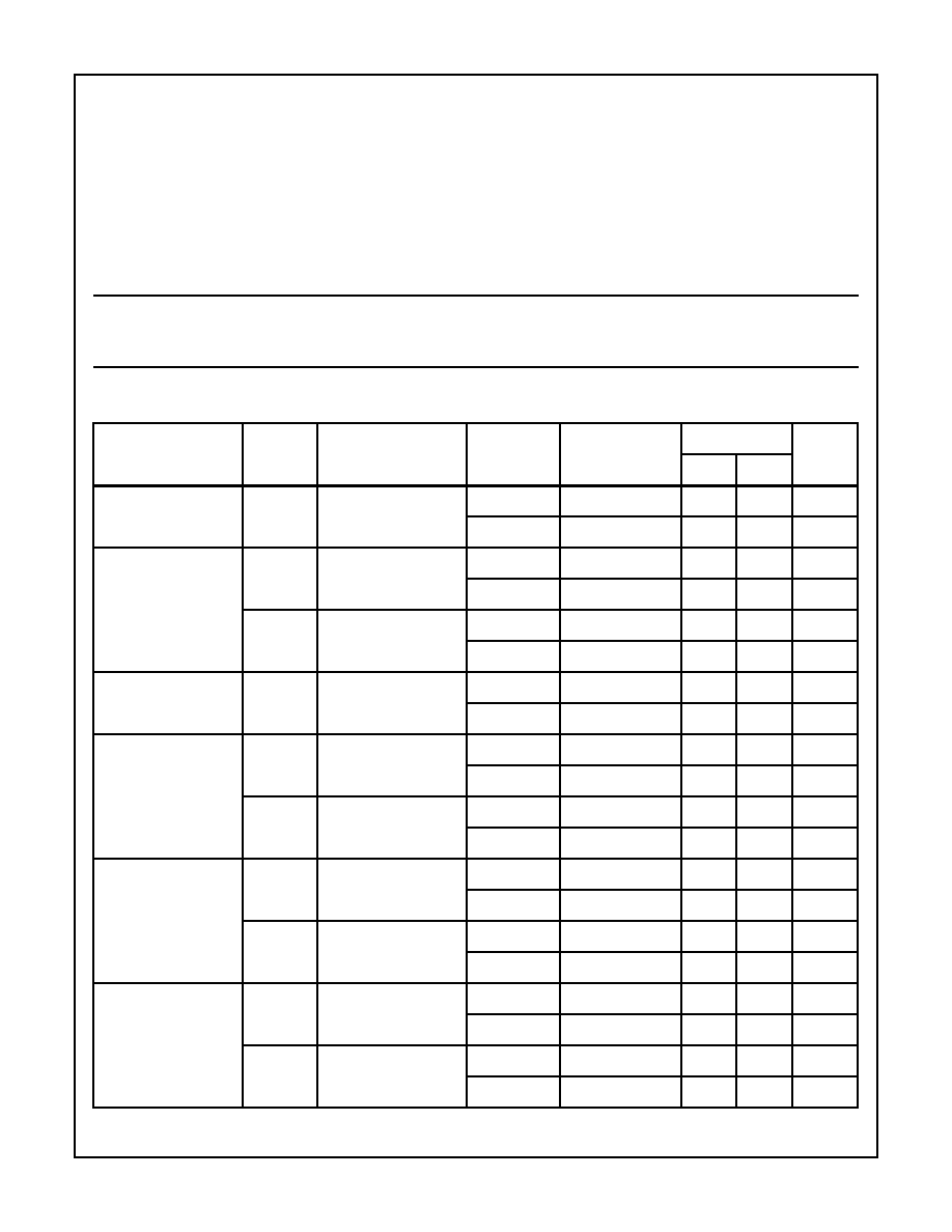
TABLE 1. DC ELECTRICAL PERFORMANCE CHARACTERISTICS
Device Tested at: V
SUPPLY
=
±
15V, R
SOURCE
= 100
, R
LOAD
= 100k
, V
OUT
= 0V, Unless Otherwise Specified.
PARAMETERS
SYMBOL
CONDITIONS
GROUP A
SUBGROUP
TEMPERATURE
LIMITS
UNITS
MIN
MAX
Input Offset Voltage
V
IO
V
CM
= 0V
1
+25
o
C
-4
4
mV
2, 3
+125
o
C, -55
o
C
-8
8
mV
Input Bias Current
+I
B
V
CM
= 0V, +R
S
= 1.1k
-R
S
= 100
1
+25
o
C
-10
10
µ
A
2, 3
+125
o
C, -55
o
C
-20
20
µ
A
-I
B
V
CM
= 0V, +R
S
= 100
-R
S
= 1.1k
1
+25
o
C
-10
10
µ
A
2, 3
+125
o
C, -55
o
C
-20
20
µ
A
Input Offset Current
I
IO
V
CM
= 0V, +R
S
= 1.1k
-R
S
= 1.1k
1
+25
o
C
-1
1
µ
A
2, 3
+125
o
C, -55
o
C
-2
2
µ
A
Common Mode Range
+CMR
V+ = 5V
V- = -25V
1
+25
o
C
10
-
V
2, 3
+125
o
C, -55
o
C
10
-
V
-CMR
V+ = 25V
V- = -5V
1
+25
o
C
-
-10
V
2, 3
+125
o
C, -55
o
C
-
-10
V
Large Signal Voltage
Gain
+A
VOL
V
OUT
= 0V and +10V
R
L
= 1k
4
+25
o
C
50
-
kV/V
5, 6
+125
o
C, -55
o
C
30
-
kV/V
-A
VOL
V
OUT
= 0V and -10V
R
L
= 1k
4
+25
o
C
50
-
kV/V
5, 6
+125
o
C, -55
o
C
30
-
kV/V
Common Mode
Rejection Ratio
+CMRR
V
CM
= 10V,
V
OUT
= -10V
V+ = 5V, V- = -25V
1
+25
o
C
90
-
dB
2, 3
+125
o
C, -55
o
C
85
-
dB
-CMRR
V
CM
= -10V,
V
OUT
= 10V
V+ = 25V, V- = -5V
1
+25
o
C
90
-
dB
2, 3
+125
o
C, -55
o
C
85
-
dB
Spec Number
511088-883
3-232
Specifications HA-2842/883
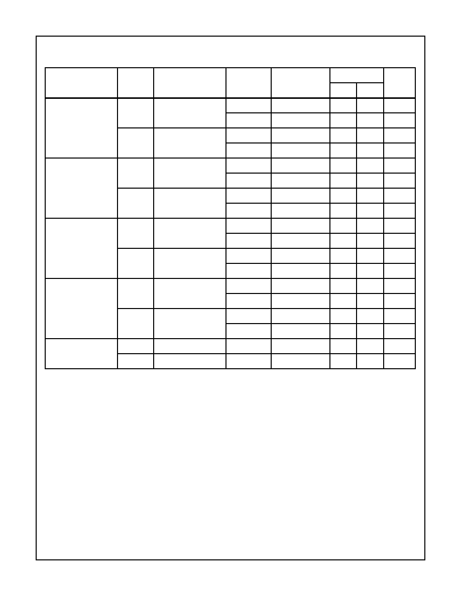
Output Voltage Swing
+V
OUT
R
L
= 1k
1
+25
o
C
10
-
V
2, 3
+125
o
C, -55
o
C
10
-
V
-V
OUT
R
L
= 1k
1
+25
o
C
-
-10
V
2, 3
+125
o
C, -55
o
C
-
-10
V
Output Current
+I
OUT
V
OUT
= -5V
Note 1
1
+25
o
C
100
-
mA
2, 3
+125
o
C, -55
o
C
100
-
mA
-I
OUT
V
OUT
= +5V
Note 1
1
+25
o
C
-
-100
mA
2, 3
+125
o
C, -55
o
C
-
-100
mA
Quiescent Power
Supply Current
+I
CC
V
OUT
= 0V
I
OUT
= 0mA
1
+25
o
C
-
15
mA
2, 3
+125
o
C, -55
o
C
-
15
mA
-I
CC
V
OUT
= 0V
I
OUT
= 0mA
1
+25
o
C
-15
-
mA
2, 3
+125
o
C, -55
o
C
-15
-
mA
Power Supply
Rejection Ratio
+PSRR
V
SUPPLY
= 10V
V+ = 10V, V- = -15V
V+ = 20V, V- = -15V
1
+25
o
C
70
-
dB
2, 3
+125
o
C, -55
o
C
70
-
dB
-PSRR
V
SUPPLY
= 10V
V+ = 15V, V- = -10V
V+ = 15V, V- = -20V
1
+25
o
C
70
-
dB
2, 3
+125
o
C, -55
o
C
70
-
dB
Offset Voltage
Adjustment
+V
IO
Adj
Note 2
1
+25
o
C
V
IO
-1
-
mV
+V
IO
Adj
Note 2
1
+25
o
C
V
IO
+1
-
mV
NOTES:
1. Maximum power dissipation, including output load conditions, must be designed to maintain the maximum junction temperature below
+175
o
C. For a 100mA load and a +125
o
C ambient, heat sinking is required.
2. Offset Adjustment range is
V
IO
(measured)
±
1mV
minimum referred to output. This test is for functionality only, to assure adjustment
through 0V.
TABLE 2. AC ELECTRICAL PERFORMANCE CHARACTERISTICS
Table 2 Intentionally Left Blank. See A.C. Specifications in Table 3.
TABLE 1. DC ELECTRICAL PERFORMANCE CHARACTERISTICS
(Continued)
Device Tested at: V
SUPPLY
=
±
15V, R
SOURCE
= 100
, R
LOAD
= 100k
, V
OUT
= 0V, Unless Otherwise Specified.
PARAMETERS
SYMBOL
CONDITIONS
GROUP A
SUBGROUP
TEMPERATURE
LIMITS
UNITS
MIN
MAX
Spec Number
511088-883

3-233
Specifications HA-2842/883
TABLE 3. ELECTRICAL PERFORMANCE CHARACTERISTICS
Device Characterized at: V
SUPPLY
=
±
15V, R
SOURCE
= 50
, R
LOAD
= 1k
, V
OUT
= 0V, A
V
= +2V/V, Unless Otherwise Specified.
PARAMETERS
SYMBOL
CONDITIONS
NOTES
TEMPERATURE
LIMITS
UNITS
MIN
MAX
Gain Bandwidth
Product
GBWP
V
O
= 200mV,
f
O
= 100kHz
1
+25
o
C
60
-
MHz
V
O
= 200mV,
f
O
= 10MHz
1
+25
o
C
70
-
MHz
Slew Rate
+SR
V
O
= -5V to +5V
1, 3
+25
o
C, -55
o
C
350
-
V/
µ
s
1, 3
+125
o
C
300
-
V/
µ
s
-SR
V
O
= +5V to -5V
1, 3
+25
o
C, -55
o
C
350
-
V/
µ
s
1, 3
+125
o
C
300
-
V/
µ
s
Full Power Bandwidth
FPBW
V
PEAK
=
+
10V
1, 2
+25
o
C, -55
o
C
5.5
-
MHz
1, 2
+125
o
C
4.7
-
MHz
Rise Time
T
R
V
O
= 0V to +200mV
C
L
10pF
1, 3
+25
o
C
-
5
ns
1, 3
-55
o
C to +125
o
C
-
7
ns
Fall Time
T
F
V
O
= 0V to -200mV
C
L
10pF
1, 3
+25
o
C
-
5
ns
1, 3
-55
o
C to +125
o
C
-
5
ns
Overshoot
+OS
V
O
= 0V to +200mV
1
+25
o
C
-
50
%
1
-55
o
C to +125
o
C
-
55
%
-OS
V
O
= 0V to -200mV
1
+25
o
C
-
50
%
1
-55
o
C to +125
o
C
-
55
%
NOTES:
1. Parameters listed in Table 3 are controlled via design or process parameters and are not directly tested at final production. These param-
eters are lab characterized upon initial design release, or upon design changes. These parameters are guaranteed by characterization
based upon data from multiple production runs which reflect lot to lot and within lot variations.
2. Full Power Bandwidth guarantee based on Slew Rate measurement using FPBW = Slew Rate/(2
V
PEAK
).
3. Measured between 10% and 90% points.
TABLE 4. ELECTRICAL TEST REQUIREMENTS
MIL-STD-883 TEST REQUIREMENTS
SUBGROUPS (SEE TABLE 1)
Interim Electrical Parameters (Pre Burn-In)
1
Final Electrical Test Parameters
1 (Note 1), 2, 3, 4, 5, 6
Group A Test Requirements
1, 2, 3, 4, 5, 6
Groups C & D Endpoints
1
NOTE:
1. PDA applies to Subgroup 1 only.
Spec Number
511088-883
3-234
Spec Number
511088-883
Die Characteristics
DIE DIMENSIONS:
77 x 81 x 19 mils
±
1 mils
1960 x 2060 x 483
µ
m
±
25.4
µ
m
METALLIZATION:
Type: Al, 1% Cu
Thickness: 16k
≈
±
2k
≈
GLASSIVATION:
Type: Nitride over Silox
Silox Thickness: 12k
≈
±
2k
≈
Nitride Thickness: 3.5k
≈
±
1.5k
≈
WORST CASE CURRENT DENSITY:
1.83 x 10
5
A/cm
2
at 56mA
SUBSTRATE POTENTIAL (Powered Up): V-
TRANSISTOR COUNT: 58
PROCESS: Bipolar Dielectric Isolation
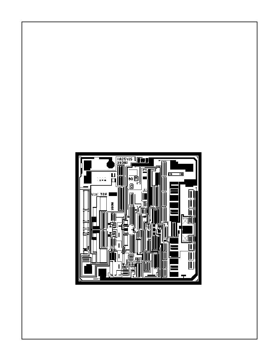
Metallization Mask Layout
HA-2842/883
V+
OUT
BAL
BAL
-IN
+IN
V-
HA-2842/883

3-235
HA-2842/883
Test Circuit
(Applies to Table 1)
Test Waveforms
SIMPLIFIED TEST CIRCUIT FOR LARGE AND SMALL SIGNAL RESPONSE (Applies to Table 3
)
MEASURED LARGE SIGNAL RESPONSE
Vertical Scale: Input = 5V/Div., Output = 5V/Div.
Horizontal Scale: 50ns/Div.
MEASURED SMALL SIGNAL RESPONSE
Vertical Scale: Input = 100mV/Div., Output = 100mV/Div.
Horizontal Scale: 50ns/Div.
S6A
1
100
S5
1
+
1
2
3
S8
1K
V-
OPEN
S9
1
2
1
V2
E
OUT
1
1K
S1
S2
S6B
1
1
0.1
100K
FOR LOOP STABILITY,
USE MIN VALUE CAPACITOR
TO PREVENT OSCILLATION
OPEN
OPEN
1K
10K
BUFFER
OPEN
OPEN
2 AC OUT
2
OPEN
100K
V1
DUT
V+
BAL
ADJ
FB
ALL RESISTORS =
±
1% (
)
ALL CAPACITORS =
±
10% (
µ
F)
1
0.1
1
2
2K
100K
100K
2K
S7A
S7B
1
2
1
2
1
2
100
10K
+
-
-1
2
2
2
-
+
-
V
IN
V
OUT
50
500
V
S
=
±
15V
A
V
= +2
C
L
10pF
500
INPUT
OUTPUT
INPUT
OUTPUT
Spec Number
511088-883

3-236
HA-2842/883
Burn-In Circuits
HA1-2842/883 CERAMIC DIP
HA7-2842/883 CERAMIC DIP
NOTES:
1. R
1
= 1M
,
±
5%, 1/4W (Min)
2. R
2
= 100k
,
±
5%, 1/4W (Min) = R
3
3. C
1
= C
2
= 0.01
µ
F/Socket (Min) or 0.1
µ
F/Row, (Min)
4. D
1
= D
2
= 1N4002 or Equivalent/Board
5.
(V+) - (V-
)
= 31V
±
1V
1
2
3
4
5
6
7
14
13
12
11
10
9
8
V-
V+
R
1
R
2
D
2
C
2
D
1
C
1
+
-
R
3
1
2
3
4
8
7
6
5
V+
D
1
C
1
R
1
V-
R
2
D
2
C
2
+
-
R
3
Spec Number
511088-883

3-237
HA-2842/883
Schematic Diagram
V+
R1
1.2K
600
R3
R6
5K
R7
5K
QP1
QP4
QN4
QN2
QP5
QP2
QN1
R4
10K
QP3
V-
QN3
R5
560
R9
5K
QN6
R8
5K
R10
170
QN9
QN8
QN5
R12
170
QN12
R14
170
QN14
QP11
QN11
QN13
QN16
QN15
R18
112
QP8
QP10
QP9
QP7
R17
5K
R15
5K
R13
112
QP6
QP12
QN7
QN10
R11
820
DZ1
300K
R2
R19
167
R20
167
R23
100
QN23
QN21
QN17
QN18
QN20
QN22
QP17
QP15
QP18
R25
10
QN19
R24
10
QN24
R21
200
R22
200
QP16
QP14
QP13
V
OUT
C1
+IN
-IN
2pF
BAL
BAL
R16
2k
Spec Number
511088-883

The information contained in this section has been developed through characterization by Intersil Corporation and is for use as application
and design information only. No guarantee is implied.
3-238
DESIGN INFORMATION
HA-2842
Wideband, High Slew Rate
High Output Current, Operational Amplifier
Typical Performance Curves
V
SUPPLY
=
±
15V, A
V
= +2, R
L
= 1k
, C
L
< 10pF, T
A
= +25
o
C, Unless Otherwise Specified.
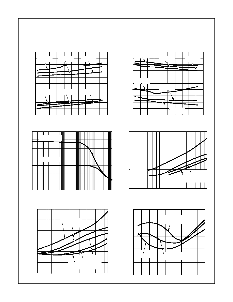
FREQUENCY RESPONSE FOR VARIOUS GAINS
GAIN BANDWIDTH PRODUCT vs SUPPLY VOLTAGE
GAIN BANDWIDTH PRODUCT vs TEMPERATURE
CMRR vs FREQUENCY
10
100
1K
10K
100K
1M
10M
100M
FREQUENCY (Hz)
GAIN (dB)
120
100
80
60
40
20
0
180
PHASE (DEGREES)
OPEN LOOP
A
VCL
= 1000
A
VCL
= 100
A
VCL
= 10
A
VCL
= 2
OPEN LOOP
A
VCL
= 1000
A
VCL
= 100
A
VCL
= 10
A
VCL
= 2
0
90
GAIN BANDWIDTH
PRODUCT (MHz)
5
6
7
8
9
10
11
12
13
14
15
SUPPLY VOLTAGE (
±
V)
90
80
70
60
50
40
30
100
60
50
40
30
90
GAIN BANDWIDTH
PRODUCT (MHz)
-60
-40
-20
0
+20
+40
+60
+80
+100 +120 +140
TEMPERATURE (
o
C)
80
70
100
110
100
90
80
70
60
50
CMRR (dB)
100
1K
10K
100K
1M
10M
FREQUENCY (Hz)
Spec Number
511088-883

DESIGN INFORMATION
(Continued)
The information contained in this section has been developed through characterization by Intersil Corporation and is for use as application
and design information only. No guarantee is implied.
3-239
HA-2842
PSRR vs FREQUENCY
INPUT NOISE vs FREQUENCY
SLEW RATE vs TEMPERATURE
SLEW RATE vs SUPPLY VOLTAGE
INPUT OFFSET VOLTAGE AND INPUT BIAS CURRENT vs
TEMPERATURE
SUPPLY CURRENT vs SUPPLY VOLTAGE
Typical Performance Curves
V
SUPPLY
=
±
15V, A
V
= +2, R
L
= 1k
, C
L
< 10pF, T
A
= +25
o
C, Unless Otherwise Specified.
90
80
70
60
50
40
30
PSRR (dB)
1K
10K
100K
1M
10M
FREQUENCY (Hz)
20
10
20
16
12
8
4
0
50
40
30
20
10
0
NOISE VOL
T
AGE (nV/
Hz)
10
100
1K
10K
100K
FREQUENCY (Hz)
NOISE CURRENT (pA/
Hz)
NOISE VOLTAGE
NOISE CURRENT
425
400
375
350
SLEW RA
TE (V/
µ
s)
-60
-40
-20
0
+20
+40
+60 +80 +100 +120 +140
TEMPERATURE (
o
C)
450
400
350
300
250
200
SLEW RA
TE (V/
µ
s)
5
6
7
8
9
10
11
12
13
14
15
SUPPLY VOLTAGE (
±
V)
8
7
6
5
4
3
INPUT BIAS CURRENT (
µ
A)
3
2
1
0
-1
-2
INPUT OFFSET VOL
T
AGE (mV)
OFFSET VOLTAGE
BIAS CURRENT
-60
-40
-20
0
+20 +40
+60
+80 +100 +120 +140
TEMPERATURE (
o
C)
16
14
12
10
8
6
4
SUPPL
Y CURRENT (mA)
5
6
7
8
9
10
11
12
13
14
15
SUPPLY VOLTAGE (
±
V)
+125
o
C
+25
o
C
-55
o
C
Spec Number
511088-883
DESIGN INFORMATION
(Continued)
The information contained in this section has been developed through characterization by Intersil Corporation and is for use as application
and design information only. No guarantee is implied.
3-240
HA-2842
POSITIVE OUTPUT SWING vs TEMPERATURE
NEGATIVE OUTPUT SWING vs TEMPERATURE
MAXIMUM UNDISTORTED OUTPUT SWING vs FREQUENCY
TOTAL HARMONIC DISTORTION vs FREQUENCY
INTERMODULATION DISTORTION vs FREQUENCY
(TWO TONE)
DIFFERENTIAL GAIN vs LOAD RESISTANCE
Typical Performance Curves
V
SUPPLY
=
±
15V, A
V
= +2, R
L
= 1k
, C
L
< 10pF, T
A
= +25
o
C, Unless Otherwise Specified.
15
10
5
2.5
POSITIVE OUTPUT SWING (V)
-60
-40
-20
0
+20 +40
+60
+80 +100 +120 +140
TEMPERATURE (
o
C)
7.5
12.5
±
15V, 1k
±
15V, 150
±
15V, 75
±
8V, 1k
±
8V, 150
±
8V, 75
-60
-40
-20
0
+20
+40
+60 +80 +100 +120 +140
TEMPERATURE (
o
C)
NEGA
TIVE OUTPUT SWING (V)
-2.5
-5
-10
-15
-7.5
-12.5
±
15V, 1k
±
15V, 150
±
15V, 75
±
8V, 1k
±
8V, 150
±
8V, 75
30
25
20
15
10
5
0
1K
10K
100K
1M
10M
100M
FREQUENCY (Hz)
V
SUPPLY
=
±
15V
V
SUPPLY
=
±
8V
OUTPUT VOL
T
AGE SWING (V
P-P
)
100K
1M
10M
-40
-50
-60
-70
-80
-90
FREQUENCY (Hz)
THD (dBc)
V
O
= 10V
P-P
V
O
= 2V
P-P
V
O
= 1V
P-P
V
O
= 0.5V
P-P
-40
-50
-60
-70
-80
-90
THIRD INTERMOD PRODUCT (dBc)
1M
10M
FREQUENCY (Hz)
V
O
= 0.25V
P-P
V
O
= 0.50V
P-P
V
O
= 1V
P-P
V
O
= 2V
P-P
V
O
= 5V
P-P
500K
0.025
0.020
0.015
0.010
0.005
0
DIFFERENTIAL GAIN (%)
100
200
300
400
500
600
700
800
900 1000
LOAD RESISTANCE (
)
V
SUPPLY
=
±
8V
V
SUPPLY
=
±
15V
V
SUPPLY
=
±
10V
Spec Number
511088-883

DESIGN INFORMATION
(Continued)
The information contained in this section has been developed through characterization by Intersil Corporation and is for use as application
and design information only. No guarantee is implied.
3-241
HA-2842
DIFFERENTIAL PHASE vs LOAD RESISTANCE
GAIN FLATNESS vs FREQUENCY (A
VCL
= 2)
GAIN BANDWIDTH PRODUCT vs LOAD RESISTANCE
SUGGESTED OFFSET VOLTAGE ADJUSTMENT
Typical Performance Curves
V
SUPPLY
=
±
15V, A
V
= +2, R
L
= 1k
, C
L
< 10pF, T
A
= +25
o
C, Unless Otherwise Specified.
0.14
0.12
0.10
0.08
0.06
0.04
0.02
DIFFERENTIAL PHASE (DEGREES)
0
100
200 300
400
500
600
700
800
900
1000
LOAD RESISTANCE (
)
V
SUPPLY
=
±
8V
V
SUPPLY
=
±
10V
V
SUPPLY
=
±
15V
0.04
0.03
0.02
0.01
0
GAIN FLA
TNESS (
±
dB)
0
1M
2M
3M
4M
5M
6M
7M
8M
9M
10M
FREQUENCY (Hz)
R
L
= 75
R
L
= 150
R
L
= 500
R
L
= 1000
80
75
70
65
GAIN BANDWIDTH PRODUCT (MHz)
0
100
200
300
400
500
600
700
800
900 1000
LOAD RESISTANCE (
)
85
+
-
V-
5K
V+
OUT
Spec Number
511088-883

3-242
All Intersil semiconductor products are manufactured, assembled and tested under ISO9000 quality systems certification.
Intersil products are sold by description only. Intersil Corporation reserves the right to make changes in circuit design and/or specifications at any time without
notice. Accordingly, the reader is cautioned to verify that data sheets are current before placing orders. Information furnished by Intersil is believed to be accurate
and reliable. However, no responsibility is assumed by Intersil or its subsidiaries for its use; nor for any infringements of patents or other rights of third parties which
may result from its use. No license is granted by implication or otherwise under any patent or patent rights of Intersil or its subsidiaries.
For information regarding Intersil Corporation and its products, see web site http://www.intersil.com
HA-2842
TYPICAL PERFORMANCE CHARACTERISTICS
Device Characterized at: V
SUPPLY
=
±
15V, R
L
= 1k
, C
L
10pF, Unless Otherwise Specified.
PARAMETERS
CONDITIONS
TEMPERATURE
TYPICAL
UNITS
Input Offset Voltage
V
CM
= 0V
+25
o
C
1
mV
Average Offset Voltage Drift
Versus Temperature
Full
13
µ
V/
o
C
Input Bias Current
V
CM
= 0V
+25
o
C
5.0
µ
A
Input Offset Current
V
CM
= 0V
+25
o
C
0.5
µ
A
Differential Input Resistance
+25
o
C
170
k
Input Noise Voltage
f
O
= 10Hz to 1MHz
+25
o
C
16
µ
V
RMS
Input Noise Voltage Density
f
O
= 1000Hz
+25
o
C
16
nV
/
Hz
Input Noise Current Density
f
O
= 1000Hz
+25
o
C
2
pA
/
Hz
Large Signal Voltage Gain
V
OUT
=
±
10V
+25
o
C
100
kV/V
Full
60
kV/V
CMRR
V
CM
=
±
10V
Full
110
dB
Gain Bandwidth Product
f = 10MHz
+25
o
C
80
MHz
Output Voltage Swing
R
L
= 1k
Full
±
11
V
Output Current
V
OUT
>
10V
Full
120
mA
Output Resistance
Open Loop
+25
o
C
8.5
Full Power Bandwidth
FPBW = SR/2
V
P
, V
P
= 10V
+25
o
C
6.0
MHz
Slew Rate
V
OUT
=
±
5V, A
V
= +2
+25
o
C
375
V/
µ
s
Rise and Fall Time
V
OUT
=
±
100mV, A
V
= +2
+25
o
C
3.5
ns
Overshoot
V
OUT
=
±
100mV, A
V
= +2
+25
o
C
20
%
PSRR
Delta V
S
=
±
10V to
±
20V
Full
80
dB
Supply Current
No Load
Full
14.2
mA
Differential Gain
R
L
= 700
+25
o
C
0.02
%
Differential Phase
R
L
= 700
+25
o
C
0.03
Degrees
Gain Flatness to 10MHz
R
L
= 75
+25
o
C
±
0.035
dB
Spec Number
511088-883