1
HA-4900, HA-4902, HA-4905
Precision Quad Comparators
The HA-4900 series are monolithic, quad, precision
comparators offering fast response time, low offset voltage,
low offset current and virtually no channel-to-channel
crosstalk for applications requiring accurate, high speed,
signal level detection. These comparators can sense signals
at ground level while being operated from either a single +5V
supply (digital systems) or from dual supplies (analog
networks) up to
±
15V. The HA-4900 series contains a unique
current driven output stage which can be connected to logic
system supplies (V
LOGIC
+ and V
LOGIC
-) to make the output
levels directly compatible (no external components needed)
with any standard logic or special system logic levels. In
combination analog/digital systems, the design employed in
the HA-4900 series input and output stages prevents
troublesome ground coupling of signals between analog and
digital portions of the system.
These comparators' combination of features make them
ideal components for signal detection and processing in data
acquisition systems, test equipment and
microprocessor/analog signal interface networks.
For military grade product, refer to the HA-4902/883 data
sheet.
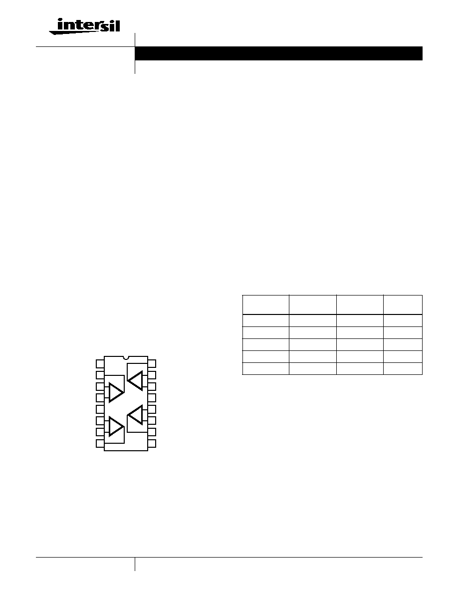
Pinout
HA-4900, HA-4902 (CERDIP)
HA-4905 (PDIP, CERDIP, SOIC)
TOP VIEW
Features
∑ Fast Response Time . . . . . . . . . . . . . . . . . . . . . . . . 130ns
∑ Low Offset Voltage . . . . . . . . . . . . . . . . . . . . . . . . . 2.0mV
∑ Low Offset Current . . . . . . . . . . . . . . . . . . . . . . . . . . .10nA
∑ Single or Dual Voltage Supply Operation
∑ Selectable Output Logic Levels
∑ Active Pull-Up/Pull-Down Output Circuit. No External
Resistors Required
Applications
∑ Threshold Detector
∑ Zero Crossing Detector
∑ Window Detector
∑ Analog Interfaces for Microprocessors
∑ High Stability Oscillators
∑ Logic System Interfaces
14
15
16
9
13
12
11
10
1
2
3
4
5
7
6
8
V
L
+
OUT 1
-IN 1
+IN 1
V-
+IN 2
OUT 2
-IN 2
OUT 4
+IN 4
V+
+IN 3
-IN 3
OUT 3
V
L
-
-IN 4
1
-
+
2
-
+
4
-
+
3
-
+
Ordering Information
PART
NUMBER
TEMP RANGE
(
o
C)
PACKAGE
PKG. NO.
HA1-4900-2
-55 to 125
16 Ld CERDIP
F16.3
HA1-4902-2
-55 to 125
16 Ld CERDIP
F16.3
HA1-4905-5
0 to 75
16 Ld CERDIP
F16.3
HA3-4905-5
0 to 75
16 Ld PDIP
E16.3
HA9P4905-5
0 to 75
16 Ld SOIC
M16.3
Data Sheet
September 1998
File Number
2855.3
CAUTION: These devices are sensitive to electrostatic discharge; follow proper IC Handling Procedures.
1-888-INTERSIL or 321-724-7143
|
Copyright
©
Intersil Corporation 1999

2
Absolute Maximum Ratings
Thermal Information
Supply Voltage (Between V+ and V- Terminals) . . . . . . . . . . . . 33V
Differential Input Voltage . . . . . . . . . . . . . . . . . . . . . . . . . . . . . . .15V
Voltage Between V
LOGIC
+ and V
LOGIC
-. . . . . . . . . . . . . . . . . . .18V
Output Current . . . . . . . . . . . . . . . . . . . . . . . . . . . . . . . . . . . . . 50mA
Power Dissipation (Notes 1, 2)
Operating Conditions
Temperature Range
HA-4900-2, HA-4902-2. . . . . . . . . . . . . . . . . . . . . -55
o
C to 125
o
C
HA-4905-5 . . . . . . . . . . . . . . . . . . . . . . . . . . . . . . . . 0
o
C to 75
o
C
Thermal Resistance (Typical, Note 3)
JA
(
o
C/W)
JC
(
o
C/W)
CERDIP Package . . . . . . . . . . . . . . . . .
85
25
PDIP Package . . . . . . . . . . . . . . . . . . .
90
N/A
SOIC Package . . . . . . . . . . . . . . . . . . .
100
N/A
Maximum Junction Temperature (Ceramic Package) . . . . . . .175
o
C
Maximum Junction Temperature (Plastic Package) . . . . . . . . .150
o
C
Maximum Storage Temperature Range . . . . . . . . . . -65
o
C to 150
o
C
Maximum Lead Temperature (Soldering 10s) . . . . . . . . . . . . 300
o
C
(SOIC - Lead Tips Only)
Die Characteristics
Back Side Potential . . . . . . . . . . . . . . . . . . . . . . . . . . . . . . . . . . V-
Number of Transistors . . . . . . . . . . . . . . . . . . . . . . . . . . . . . . . 137
Die Size . . . . . . . . . . . . . . . . . . . . . . . . . . . . . . 95 mils x 105 mils
CAUTION: Stresses above those listed in "Absolute Maximum Ratings" may cause permanent damage to the device. This is a stress only rating and operation of the
device at these or any other conditions above those indicated in the operational sections of this specification is not implied.
NOTES:
1. Maximum power dissipation, including output load, must be designed to maintain the junction temperature below 175
o
C for ceramic packages,
and below 150
o
C for plastic packages.
2. Total Power Dissipation (T.P.D.) is the sum of individual dissipation contributions of V+, V- and V
LOGIC
shown in curves of Power Dissipation
vs Supply Voltages (see Performance Curves). The calculated T.P.D. is then located on the graph of Maximum Allowable Package Dissipation
vs Ambient Temperature to determine ambient temperature operating limits imposed by the calculated T.P.D. (See Performance Curves). For
instance, the combination of +15V, -15V, +5V, 0V (V+, V-, V
LOGIC
+, V
LOGIC
-) gives a T.P.D. of 350mW, the combination +15V, -15V, +15V,
0V gives a T.P.D. of 450mW.
3.
JA
is measured with the component mounted on an evaluation PC board in free air.
Electrical Specifications
V
SUPPLY
= 15V, V
LOGIC
+ = 5V, V
LOGIC
- = GND
PARAMETER
TEMP
(
o
C)
HA-4900-2
-55
o
C to 125
o
C
HA-4902-2
-55
o
C to 125
o
C
HA-4905-5
0
o
C to 75
o
C
UNITS
MIN
TYP
MAX
MIN
TYP
MAX
MIN
TYP
MAX
INPUT CHARACTERISTICS
Offset Voltage (Note 4)
25
-
2
3
-
2
5
-
4
7.5
mV
Full
-
-
4
-
-
8
-
-
10
mV
Offset Current
25
-
10
25
-
10
35
-
25
50
nA
Full
-
-
35
-
-
45
-
-
70
nA
Bias Current (Note 5)
25
-
50
75
-
50
150
-
100
150
nA
Full
-
-
150
-
-
200
-
-
300
nA
Input Sensitivity (Note 6)
25
-
-
V
IO
+
0.3
-
-
V
IO
+
0.5
-
-
V
IO
+
0.5
mV
Full
-
-
V
IO
+
0.4
-
-
V
IO
+
0.6
-
-
V
IO
+
0.7
mV
Common Mode Range
Full
V-
-
(V+) -
2.4
V-
-
(V+) -
2.6
V-
-
(V+) -
2.4
V
Differential Input Resistance
25
-
250
-
-
250
-
-
250
-
M
TRANSFER CHARACTERISTICS
Large Signal Voltage Gain
25
-
400
-
-
400
-
-
400
-
kV/V
Response Time (t
PD
(0))
(Note 7)
25
-
130
200
-
130
200
-
130
200
ns
Response Time (t
PD
(1))
(Note 7)
25
-
180
215
-
180
215
-
180
215
ns
HA-4900, HA-4902, HA-4905
3
OUTPUT CHARACTERISTICS
Output Voltage Level
Logic "Low State" (V
OL
)
(Note 8)
Full
-
0.2
0.4
-
0.2
0.4
-
0.2
0.4
V
Logic "High State" (V
OH
)
(Note 8)
Full
3.5
4.2
-
3.5
4.2
-
3.5
4.2
-
V
Output Current
I
SINK
Full
3.0
-
-
3.0
-
-
3.0
-
-
mA
I
SOURCE
Full
3.0
-
-
3.0
-
-
3.0
-
-
mA
POWER SUPPLY CHARACTERISTICS
Supply Current, IPS (+)
25
-
6.5
20
-
6.5
20
-
7
20
mA
Supply Current, IPS (-)
25
-
4
8
-
4
8
-
5
8
mA
Supply Current, IPS (Logic)
25
-
3.5
4
-
3.5
4
-
3.5
4
mA
Supply Voltage Range
V
LOGIC
+ (Note 2)
Full
0
-
+15.0
0
-
+15.0
0
-
+15.0
V
V
LOGIC
- (Note 2)
Full
-15.0
-
0
-15.0
-
0
-15.0
-
0
V
NOTES:
4. Minimum differential input voltage required to ensure a defined output state.
5. Input bias currents are essentially constant with differential input voltages up to
±
9V. With differential input voltages from
±
9V to
±
15V, bias cur-
rent on the more negative input can rise to approximately 500
µ
A. This will also cause higher supply currents.
6. V
CM
= 0V. Input sensitivity is the worst case minimum differential input voltage required to guarantee a given output logic state. This parameter
includes the effects of offset voltage and voltage gain.
7. For t
PD
(1); 100mV input step, -10mV overdrive. For t
PD
(0); -100mV input step, 10mV overdrive. Frequency
100Hz; Duty Cycle
50%; Invert-
ing input driven. See Figure 1 for Test Circuit. All unused inverting inputs tied to +5V.
8. For V
OH
and V
OL
: I
SINK
= I
SOURCE
= 3.0mA. For other values of V
LOGIC
; V
OH
(Min) = V
LOGIC
+ -1.5V.
Electrical Specifications
V
SUPPLY
= 15V, V
LOGIC
+ = 5V, V
LOGIC
- = GND (Continued)
PARAMETER
TEMP
(
o
C)
HA-4900-2
-55
o
C to 125
o
C
HA-4902-2
-55
o
C to 125
o
C
HA-4905-5
0
o
C to 75
o
C
UNITS
MIN
TYP
MAX
MIN
TYP
MAX
MIN
TYP
MAX
Test Circuit and Waveform
FIGURE 1.
DUT
-
+
+15V
+5V
-15V
V
OUT
100mV
OVERDRIVE
t
PD
(0)
1.5V
t
PD
(0)
t = 0
V
TH
= 0V
INPUT
OUTPUT
100mV
OVERDRIVE
1.5V
t
PD
(1)
t = 0
V
TH
= 0V
t
PD
(1)
HA-4900, HA-4902, HA-4905
4
Applying the HA-4900 Series Comparators
Supply Connections
This device is exceptionally versatile in working with most
available power supplies. The voltage applied to the V+ and V-
terminals determines the allowable input signal range; while the
voltage applied to the V
L
+ and V
L
- determines the output
swing. In systems where dual analog supplies are available,
these would be connected to V+ and V-, while the logic supply
and return would be connected to V
LOGIC
+ and V
LOGIC
-. The
analog and logic supply commons can be connected together
at one point in the system, since the comparator is immune to
noise on the logic supply ground. A negative output swing may
be obtained by connecting V
L
+ to ground and V
L
- to a negative
supply. Bipolar output swings (15V
P-P
, Max) may be obtained
using dual supplies. In systems where only a single logic supply
is available (+5V to 15V), V+ and V
LOGIC
+ may be connected
together to the positive supply while V- and V
LOGIC
- are
grounded. If an input signal could swing negative with respect
the V- terminal, a resistor should be connected in series with
the input to limit input current to < 5mA since the C-B junction of
the input transistor would be forward biased.
Unused Inputs
Inputs of unused comparator sections should be tied to a
differential voltage source to prevent output "chatter."
Crosstalk
Simultaneous high frequency operation of all other channels
in the package will not affect the output logic state of a given
channel, provided that its differential input voltage is
sufficient to define a given logic state (
V
IN
±
V
OS
). Low
level or high impedance input lines should be shielded from
other signal sources to reduce crosstalk and interference.
Power Supply Decoupling
Decouple all power supply lines with 0.01
µ
F ceramic capacitors
to ground line located near the package to reduce coupling
between channels or from external sources.
Response Time
Fast rise time (<200ns) input pulses of several volts
amplitude may result in delay times somewhat longer than
those illustrated for 100mV steps. Operating speed is
optimized by limiting the maximum differential input voltage
applied, with resistor-diode clamping networks.
Typical Applications
Data Acquisition System
In this circuit the HA-4900 series is used in conjunction with
a D to A converter to form a simple, versatile, multi-channel
analog input for a data acquisition system. In operation the
processor first sends an address to the D to A, then the
processor reads the digital word generated by the
comparator outputs. To perform a simple comparison, the
processor sets the D to A to a given reference level, then
examines one or more comparator outputs to determine if
their inputs are above or below the reference. A window
comparison consists of two such cycles with 2 reference
levels set by the D to A. One way to digitize the inputs would
be for the processor to increment the D to A in steps. The D
to A address, as each comparator switches, is the digitized
level of the input. While stairstepping the D to A is slower
than successive approximation, all channels are digitized
during one staircase ramp.
Schematic Diagram
Q
9D
BIAS 2
ONE FOURTH ONLY
R
20D
1k
R
20C
1k
R
20B
1k
R
20A
1k
Q
9C
Q
9B
Q
9A
R
21
1k
Q
10
D
9A
BIAS 1
Q
5
Q
4
D
4A
D
4B
Q
4C
Q
3
R
16
540
PR
1
200k
R
10
4k
Q
2
Q
1
R
9
4k
BIAS 3
BIAS 4
Q
11
+IN
Q
17
Q
18
Q
12
Q
13
R
1
500
R
2
13k
R
3
1k
Q
19
Q
20
Q
14
R
4
1k
Q
21
Q
22
-IN
M
N1
R
7
2.5k
R
6
2.5k
Q
16
Q
7
Q
23
R
5
360
M
N2
M
N3
Q
24
Q
25
R
18
664
Q
38
M
N4
D
45
D
11A
Q
26
R
17
19k
R
14
5k
Q
33
Q
34
Q
36
Q
37
Q
30
Q
28
R
11
8k
R
15
8k
Q
31
R
23
100
R
24
14k
D
29B
Q
29
Q
29A
R
22
100
R
12
8k
Q
32
M
N6
M
N5
V
LOGIC
-
OUT
V
LOGIC
+
V-
V+
Q
15
D
35
D
39
HA-4900, HA-4902, HA-4905
5
Logic Level Translators
The HA-4900 series comparators can be used as versatile
logic interface devices as shown in the circuits above.
Negative logic devices may also be interfaced with
appropriate supply connections. If separate supplies are
used for V- and V
LOGIC
-, these logic level translators will
tolerate several volts of ground line differential noise.
RS-232 To CMOS Line Receiver
This RS-232 type line receiver to drive CMOS logic uses a
Schmitt trigger feedback network to give about 1V input
hysteresis for added noise immunity. A possible problem in
an interface which connects two equipments, each plugged
into a different AC receptacle, is that the power line voltage
may appear at the receiver input when the interface
connection is made or broken. The two diodes and a 3W
input resistor will protect the inputs under these conditions.
Window Detector
The high switching speed, low offset current and low offset
voltage of the HA-4900 series makes this window detector
circuit extremely well suited to applications requiring fast,
accurate, decision-making. The circuit above is ideal for
industrial process system feedback controllers or "out-of-
limit" alarm indicators.
Oscillator/Clock Generator
This self-starting fixed frequency oscillator circuit gives
excellent frequency stability. R
1
and C
1
comprise the
frequency determining network while R
2
provides the
regenerative feedback. Diode D
1
enhances the stability by
compensating for the difference between V
OH
and
V
SUPPLY
. In applications where a precision clock generator
up to 100kHz is required, such as in automatic test
equipment, C
1
may be replaced by a crystal.
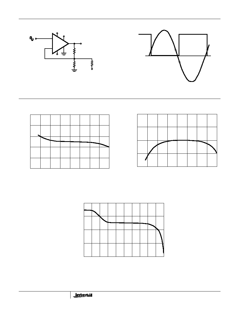
Schmitt Trigger
(Zero Crossing Detector With Hysteresis)
This circuit has a 100mV hysteresis which can be used in
applications where very fast transition times are required at
the output even though the signal input is very slow. The
hysteresis loop also reduces false triggering due to noise on
the input. The waveforms below show the trip points
developed by the hysteresis loop.
MEMORY
MICRO-
PROCESSOR
INTERF
A
C
E
INTERF
A
C
E
D/A
COMPARATORS
PROCESSOR
LA
TCH
ANALOG
INPUTS
ANALOG INPUT MODULE
1/4
HA-4900
+
-
4.7k
V
L
+
1N914s
+5.0V
1/4
HA-4900
+
-
TTL TO CMOS
1/4
HA-4900
+
-
10k
V+
+5.0V
1/4
HA-4900
+
-
CMOS TO TTL
+5V TO +15V
10k
1/4
HA-4900
+
-
+10V
4.7k
3W
1k
1N4001s
56k
51k
1k
+
-
V
L
+
+15V
+
-
-15V
1/2 HA-4900
INPUT
LOW REF
HIGH REF
HIGH
LOW
IN
WINDOW
+5.0V
1/4 HD-74C02
1/4
HA-4900
+
-
V+
150k
150k
R
2
150k
V+
R
1
50k
C
1
f
1
2.1R
1
C
1
------------------------
D
1
1N914
HA-4900, HA-4902, HA-4905
6
INPUT TO OUTPUT WAVEFORM SHOWING HYSTERESIS TRIP
POINTS
+15V
R
1
100
-15V
+5V
R
3
13k
-15V
V
OH
4.2V
R
2
2k
1/4
HA-4900
+
-
0V
V
TRIP
+
V
TRIP
-
V
OH
Typical Performance Curves
T
A
= 25
o
C, V
S
=
±
15V, V
LOGIC
+ = 5V, V
LOGIC
- = 0V, Unless Otherwise Specified
FIGURE 2. INPUT BIAS CURRENT vs TEMPERATURE
FIGURE 3. INPUT OFFSET CURRENT vs TEMPERATURE
FIGURE 4. INPUT BIAS CURRENT vs COMMON MODE INPUT VOLTAGE (V
DIFF
= 0V)
INPUT BIAS CURRENT (nA)
100
80
60
40
20
0
-55
-25
0
25
50
75
100
125
TEMPERATURE (
o
C)
15
10
5
0
INPUT OFFSET CURRENT (nA)
-55
-25
0
25
50
75
100
125
TEMPERATURE (
o
C)
-15
-12
-9
-6
-3
0
+3
+6
+9
+12
+15
COMMON MODE INPUT VOLTAGE
80
60
40
20
0
INPUT BIAS CURRENT (nA)
HA-4900, HA-4902, HA-4905

7
FIGURE 5. SUPPLY CURRENT vs TEMPERATURE (FOR
±
15V
SUPPLIES AND +5V LOGIC SUPPLY)
FIGURE 6. SUPPLY CURRENT vs TEMPERATURE (FOR SINGLE
+5V OPERATION)
FIGURE 7. RESPONSE TIME FOR VARIOUS INPUT OVERDRIVES
FIGURE 8. MAXIMUM PACKAGE DISSIPATION vs AMBIENT
TEMPERATURE
FIGURE 9. POWER DISSIPATION vs SUPPLY VOLTAGE (NO
LOAD CONDITION)
Typical Performance Curves
T
A
= 25
o
C, V
S
=
±
15V, V
LOGIC
+ = 5V, V
LOGIC
- = 0V, Unless Otherwise Specified (Continued)
-50
-25
0
25
50
75
100
125
TEMPERATURE (
o
C)
12
10
8
6
4
2
0
SUPPL
Y CURRENT (mA)
V
LOGIC
+ = 5V
V
LOGIC
- = GND
I
PS
+, V
OUT
= L
I
PS
+, V
OUT
= H
I
PS
-, V
OUT
= L
I
PS
-, V
OUT
= H
I
PS
L, V
OUT
= L
I
PS
L, V
OUT
= H
V
S
=
±
15V
-50
-25
0
25
50
75
100
125
TEMPERATURE (
o
C)
5
4
3
2
1
0
SUPPL
Y CURRENT (mA)
V+ = 5V, V- = GND
V
LOGIC
+ = 5V
V
LOGIC
- = GND
I
PS
L, V
OUT
= H
I
PS
+, V
OUT
= H
I
PS
+, V
OUT
= L
I
PS
L, V
OUT
= L
6
7
5
4
3
2
1
0
0
-100mV
V
OUT
(V)
V
IN
0
100
200
300
400
TIME (ns)
OVERDRIVE = 20mV
OVERDRIVE = 5mV
OVERDRIVE = 2mV
5
4
3
2
1
0
+100mV
V
OUT
(V)
V
IN
0
0
100
200
300
400
TIME (ns)
OVERDRIVE = 20mV
OVERDRIVE = 5mV
OVERDRIVE = 2mV
0
25
50
75
100
125
TEMPERATURE (
o
C)
2.0
1.75
1.50
1.25
1.0
0.75
0.50
0.25
0
P
A
CKA
GE DISSIP
A
TION (W)
CERDIP
PDIP
SOIC
PO
WER DISSIP
A
TION (mW)
250
200
150
100
50
0
2
4
6
8
10
12
14
SUPPLY VOLTAGE (V)
V+
V-
V
LOGIC
+
0
HA-4900, HA-4902, HA-4905

8
All Intersil semiconductor products are manufactured, assembled and tested under ISO9000 quality systems certification.
Intersil semiconductor products are sold by description only. Intersil Corporation reserves the right to make changes in circuit design and/or specifications at any time with-
out notice. Accordingly, the reader is cautioned to verify that data sheets are current before placing orders. Information furnished by Intersil is believed to be accurate and
reliable. However, no responsibility is assumed by Intersil or its subsidiaries for its use; nor for any infringements of patents or other rights of third parties which may result
from its use. No license is granted by implication or otherwise under any patent or patent rights of Intersil or its subsidiaries.
For information regarding Intersil Corporation and its products, see web site www.intersil.com
Sales Office Headquarters
NORTH AMERICA
Intersil Corporation
P. O. Box 883, Mail Stop 53-204
Melbourne, FL 32902
TEL: (321) 724-7000
FAX: (321) 724-7240
EUROPE
Intersil SA
Mercure Center
100, Rue de la Fusee
1130 Brussels, Belgium
TEL: (32) 2.724.2111
FAX: (32) 2.724.22.05
ASIA
Intersil (Taiwan) Ltd.
7F-6, No. 101 Fu Hsing North Road
Taipei, Taiwan
Republic of China
TEL: (886) 2 2716 9310
FAX: (886) 2 2715 3029
HA-4900, HA-4902, HA-4905