
1
HA-5134
4MHz, Precision, Quad Operational
Amplifier
The HA-5134 is a precision quad operational amplifier that is
pin compatible with the OP-400, LT1014, OP11, RM4156,
and LM148 as well as the HA-4741. Each amplifier features
guaranteed maximum values for offset voltage of 200
µ
V,
offset voltage drift of 2
µ
V/
o
C, and offset current of 75nA over
the full temperature range while CMRR/PSRR is guaranteed
greater than 94dB and A
VOL
is guaranteed above 500kV/V
over the full temperature range.
Precision performance of the HA-5134 is enhanced by a
noise voltage density of 7nV/
Hz at 1kHz, noise current
density of 1pA/
Hz at 1kHz and channel separation of
120dB. Each unity-gain stable quad amplifier is fabricated
using the dielectric isolation process to assure performance
in the most demanding applications.
The HA-5134 is ideal for compact circuits such as
instrumentation amplifiers, state-variable filters, and low-
level transducer amplifiers. Other applications include
precision data acquisition, precision integrators, and
accurate threshold detectors in designs where board space
is a limitation.
For military grade product, refer to the HA-5134/883 data sheet.
Features
∑ Low Offset Voltage . . . . . . . . . . . . . . . . . . . . 200
µ
V (Max)
∑ Low Offset Voltage Drift . . . . . . . . . . . . . . . 2
µ
V/
o
C (Max)
∑ High Channel Separation . . . . . . . . . . . . . . . . . . . . 120dB
∑ Low Noise. . . . . . . . . . . . . . . . . . . . . . . . . . . . . . 7nV/
Hz
∑ Unity Gain Bandwidth. . . . . . . . . . . . . . . . . . . . . . . . 4MHz
∑ High CMRR/PSRR . . . . . . . . . . . . . . . . . . . . . 120dB (Typ)
Applications
∑ Instrumentation Amplifiers
∑ State-Variable Filters
∑ Precision Integrators
∑ Threshold Detectors
∑ Precision Data Acquisition Systems
∑ Low-Level Transducer Amplifiers
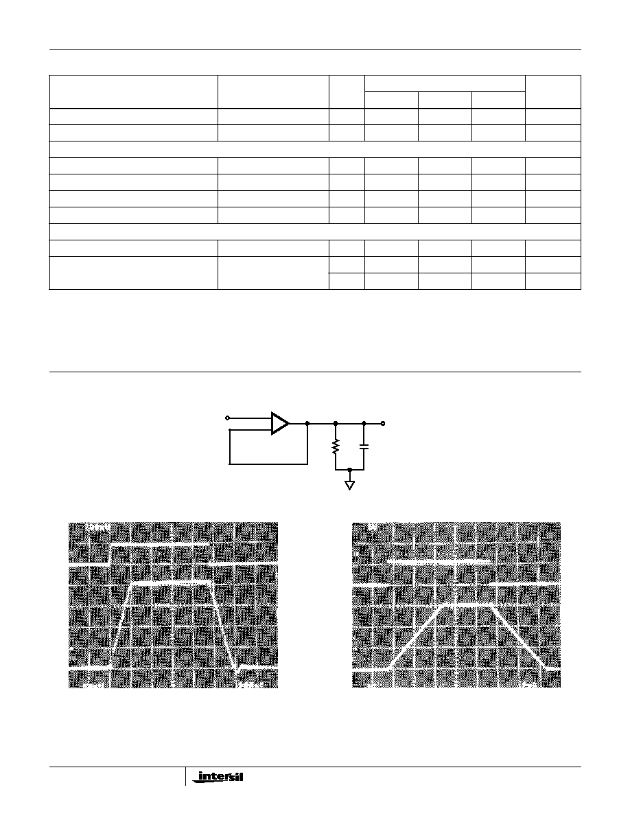
Pinout
HA-5134
(CERDIP)
TOP VIEW
Ordering Information
PART NUMBER
TEMP.
RANGE (
o
C)
PACKAGE
PKG.
NO.
HA1-5134-5
0 to 75
14 Ld CERDIP
F14.3
1
2
3
4
5
6
7
14
13
12
11
10
9
8
V-
OUT 3
OUT 4
V+
1
+
4
+
2
+
3
+
OUT 1
-IN 1
OUT 2
+IN 1
+IN 2
-IN 2
-IN 4
+IN 4
+IN 3
-IN 3
-
-
-
-
Data Sheet
August 1998
File Number
2926.3
CAUTION: These devices are sensitive to electrostatic discharge; follow proper IC Handling Procedures.
1-888-INTERSIL or 321-724-7143
|
Copyright
©
Intersil Corporation 1999

2
Absolute Maximum Ratings
Thermal Information
Voltage Between V+ and V- Terminals. . . . . . . . . . . . . . . . . . . . 40V
Differential Input Voltage (Note 2) . . . . . . . . . . . . . . . . . . . . . . . . 6V
Output Current . . . . . . . . . . . . . . . . . . . . Full Short Circuit Protection
Operating Conditions
Temperature Range
HA-5134-5 . . . . . . . . . . . . . . . . . . . . . . . . . . . . . . . . 0
o
C to 75
o
C
Thermal Resistance (Typical, Note 1)
JA
(
o
C/W)
JC
(
o
C/W)
CERDIP Package . . . . . . . . . . . . . . . . .
80
30
Maximum Junction Temperature (Note 3) . . . . . . . . . . . . . . . . 175
o
C
Maximum Storage Temperature Range . . . . . . . . . . -65
o
C to 150
o
C
Maximum Lead Temperature (Soldering 10s) . . . . . . . . . . . . 300
o
C
CAUTION: Stresses above those listed in "Absolute Maximum Ratings" may cause permanent damage to the device. This is a stress only rating and operation of the
device at these or any other conditions above those indicated in the operational sections of this specification is not implied.
NOTES:
1.
JA
is measured with the component mounted on an evaluation PC board in free air.
2. For differential input voltages greater than 6V, the input current must be limited to 25mA to protect the back-to-back input diodes.
3. Maximum power dissipation, including output load, must be designed to maintain the maximum junction temperature below 175
o
C.
Electrical Specifications
V
SUPPLY
=
±
15V, R
L
= 2k
, C
L
= 50pF, R
S
100
,
Unless Otherwise Specified
PARAMETER
TEST CONDITIONS
TEMP
(
o
C)
HA-5134-5
UNITS
MIN
TYP
MAX
INPUT CHARACTERISTICS
Offset Voltage
25
-
50
200
µ
V
Full
-
75
350
µ
V
Average Offset Voltage Drift
Full
-
0.3
2
µ
V/
o
C
Bias Current
25
-
±
10
±
50
nA
Full
-
±
20
±
75
nA
Offset Current
25
-
10
50
nA
Full
-
15
75
nA
Average Offset Current Drift
Full
-
0.05
-
nA/
o
C
Common Mode Range
Full
±
10
-
-
V
Differential Input Resistance
25
-
30
-
M
Input Noise Voltage
0.1Hz to 10Hz
25
-
0.2
-
µ
V
P-P
Input Noise Voltage Density
f = 10Hz
25
-
10
-
nV/
Hz
f = 100Hz
-
7.5
-
nV/
Hz
f = 1kHz
-
7
-
nV/
Hz
Input Noise Current Density
f = 10Hz
25
-
3
-
pA/
Hz
f = 100Hz
-
1.5
-
pA/
Hz
f = 1kHz
-
1
-
pA/
Hz
TRANSFER CHARACTERISTICS
Large Signal Voltage Gain
V
OUT
=
±
10V
25
800
1200
-
kV/V
Full
500
750
-
kV/V
Common Mode Rejection Ratio
V
CM
=
±
10V
25
100
120
-
dB
Full
94
115
-
dB
Minimum Stable Gain
25
1
-
-
V/V
Unity-Gain Bandwidth
25
-
4
-
MHz
OUTPUT CHARACTERISTICS
Output Voltage Swing
Full
12
13.5
-
V
Output Current
25
-
20
-
mA
HA-5134
3
Full Power Bandwidth (Note 4)
25
12
16
-
kHz
Channel Separation (Note 7)
V
OUT
=
±
10V
25
120
136
-
dB
TRANSIENT RESPONSE (Note 5)
Rise Time
A
V
= +1, V
OUT
= 200mV
25
-
200
400
ns
Slew Rate
A
V
= +1
25
0.75
1.0
-
V/
µ
s
Overshoot
A
V
= +1
25
-
20
40
%
Settling Time (Note 6)
25
-
13
-
µ
s
POWER SUPPLY CHARACTERISTICS
Supply Current
All Amps
Full
-
6.5
8
mA
Power Supply Rejection Ratio
V
S
=
±
5V to
±
18V
25
100
120
-
dB
Full
94
115
-
dB
NOTES:
4. Full power bandwidth guaranteed based on slew rate measurement using:
.
5. Refer to Test Circuits section of the data sheet.
6. Specified to 0.01% of a 10V step, A
V
= -1.
7. Guaranteed but not tested.
Electrical Specifications
V
SUPPLY
=
±
15V, R
L
= 2k
, C
L
= 50pF, R
S
100
,
Unless Otherwise Specified (Continued)
PARAMETER
TEST CONDITIONS
TEMP
(
o
C)
HA-5134-5
UNITS
MIN
TYP
MAX
FPBW
Slew Rate
2
V
PEAK
-------------------------------
; V
PEAK
10V
=
=
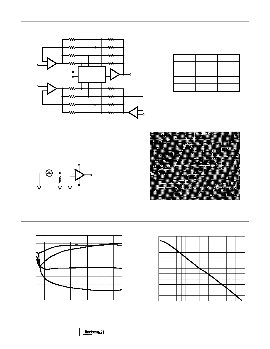
Test Circuits and Waveforms
FIGURE 1. SLEW RATE AND TRANSIENT RESPONSE TEST CIRCUIT
Vertical: 50mV/Div.,
Horizontal: 200ns/Div.
T
A
= 25
o
C, V
S
=
±
15V, A
V
= +1, R
L
= 2k
,
C
L
= 50pF
SMALL SIGNAL RESPONSE
Vertical: 2V/Div.,
Horizontal: 2
µ
s/Div.
T
A
= 25
o
C, V
S
=
±
15V, A
V
= +1, R
L
= 2k
,
C
L
= 50pF
LARGE SIGNAL RESPONSE
IN
50pF
OUT
2k
+
-
HA-5134

4
Schematic Diagram
(Each Amplifier)
FIGURE 2. SETTLING TIME CIRCUIT
T
A
= 25
o
C, V
S
=
±
15V, A
V
= 1000
e
n
= 0.167
µ
V
P-P
0.05
µ
V/Div., 1s/Div.
PEAK-TO-PEAK NOISE 0.1Hz TO 10Hz
Test Circuits and Waveforms
(Continued)
+
-
A.U.T.
+15V
-15V
2k
50pF
V
OUT
5k
5k
2k
V
IN
2k
TO
OSCILLOSCOPE
2N4416
+15V
NOTES:
8. A
V
= -1.
9. Feedback and summing resistors should be 0.1% matched.
10. Clipping diodes are optional. HP5082-2810 recommended.
Q
P2
Q
N1
R
2
Q
N3
R
1
Q
N2
Q
N4
Q
N11
Q
P1
Q
P5
Q
P7
Q
P4
Q
P3
V+
Q
N5
Q
N8
Q
N10
Q
N12
Q
N14
Q
N13
Q
N15
Q
P10
R
3
R
4
C
2
Q
N16
Q
N17
Q
N18
Q
P8
C
1
R
5
Q
N19
Q
P13
Q
P12
Q
P11
Q
N20
R
7
Q
N23
Q
P14
OUT
V-
Q
N22
R
8
Q
N21
R
6
Q
P6
+IN
Q
N9
Q
P9
D
2
D
1
-IN
Q
N26
Q
N25
Q
N24
Q
N7
Q
N6
HA-5134

5
Application Information
Power Supply Decoupling
Although not absolutely necessary, it is recommended that
all power supply lines be decoupled with 0.01
µ
F ceramic
capacitors to ground. Decoupling capacitors should be
located as near to the amplifier terminals as possible.
Considerations For Prototyping
The following list of recommendations are suggested for
prototyping.
1. Resolving low level signals requires minimizing leakage
currents caused by external circuitry. Use of quality insulating
materials, thorough cleaning of insulating surfaces and
implementation of moisture barriers when required is
suggested.
2. Error voltages generated by thermocouples formed between
dissimilar metals in the presence of temperature gradients
should be minimized. Isolation of low level circuitry from heat
generating components is recommended.
3. Shielded cable input leads, guard rings and shield drivers are
recommended for the most critical applications.
Typical Applications
T
A
= 25
o
C, V
S
=
±
15V, A
V
= 1, R
L
= 10k
20mV/Div., 1
µ
s/Div.
V
OUT
=
±
10V, R
LOAD
= 50
C
LOAD
= 0.01
µ
F, A
V
= 3, V
S
=
±
15V
Top: Input, 2V/Div., 20
µ
s/Div.
Bottom: Output, 5V/Div, 20
µ
s/Div.
FIGURE 3. SMALL SIGNAL TRANSIENT RESPONSE
(C
LOAD
= 1nF)
TRANSIENT RESPONSE OF APPLICATION CIRCUIT #1
FIGURE 4. APPLICATION CIRCUIT #1: INSTRUMENTATION AMPLIFIER WITH POWER OUTPUT
+
V
O
1nF
10k
-
NOTES:
11.
.
12. 10
- 100
recommended for short circuit limiting.
13. When driving heavy loads the HA-5002 may
contribute to thermal errors. Proper thermal shielding
is recommended.
A
V
≠
1
2R
R
G
--------
+
R
2
R
1
-------
=
+
50
1
/
4
HA-5134
+
1
/
4
HA-5134
R
R
G
R
1
/
4
HA-5134
+
HA-
5002
-15V
+15V
R
1
R
2
(NOTE 12)
(NOTE 12)
R
1
R
2
0.01
µ
F
HA-5134
6
FIGURE 5. APPLICATION CIRCUIT #2: PROGRAMMABLE GAIN AMPLIFIER
NOTE: If differential input voltages greater than 6V are present, input
current must be limited to less than 25mA.
Horizontal: 50
µ
s/Div.
V
IN
=
±
25mV, V
OUT
=
±
14V
FIGURE 6. APPLICATION CIRCUIT #3: PRECISION COMPARATOR
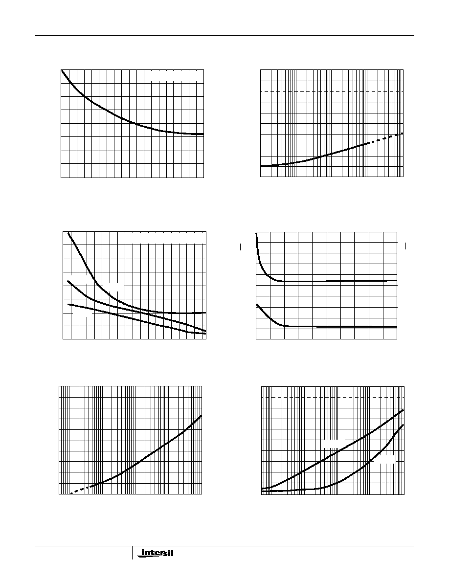
Typical Performance Curves
FIGURE 7. V
IO
WARM-UP DRIFT
FIGURE 8. INPUT OFFSET VOLTAGE vs TEMPERATURE
Typical Applications
(Continued)
G
1
G
0
A
V
0
0
-1
0
1
-2
1
0
-4
1
1
-8
High A
VOL
of HA-5134 reduces gain error.
Gain Error
0.004% at A
V
= 8.
1
/
4
HA-5134
1
/
4
HA-5134
G
1
1
/
4
HA-5134
V
IN
V
IN
G
0
R
R
R
R
8R
4R
2R
R
R
4R
2R
R
R
R
R
8R
+
V
REF
1
/
4
HA-5134
V
OUT
1B 2B 3B 4B
1A 2A 3A 4A
HI-509
-
+
-
+
-
+
-
+
1
/
4
HA-5134
OUTPUT
(TOP TRACE)
+15V
-15V
50
PULSE
GEN.
V
IN
(BOTTOM TRACE)
-
TIME (MINUTES)
0
2
4
6
8
10
-6
-5
-4
-3
-2
0
-1
1
2
T
A
= 25
o
C, V
S
=
±
15V
OFFSET CHANGE (
µ
V)
TEMPERATURE (
o
C)
0
20
40
60
80
120
-60
-50
-40
0
10
30
20
40
50
OFFSET V
O
L
T
A
GE (
µ
V)
100
-20
-40
-60
60
-30
-20
-10
HA-5134
7
FIGURE 9. OFFSET CURRENT vs TEMPERATURE
FIGURE 10. CHANNEL SEPARATION vs FREQUENCY
FIGURE 11. REJECTION RATIOS vs TEMPERATURE
FIGURE 12. NOISE DENSITY vs FREQUENCY
FIGURE 13. CMRR vs FREQUENCY
FIGURE 14. PSRR vs FREQUENCY
Typical Performance Curves
(Continued)
TEMPERATURE (
o
C)
0
20
40
60
80
120
-6
-5
-4
0
1
OFFSET CURRENT (nA)
100
-20
-40
-60
2
-3
-2
-1
A
CL
= +1, V
S
=
±
15V
FREQUENCY (Hz)
100
1K
100K
120
0
CHANNEL SEP
ARA
TION (dB)
10K
10
80
40
160
TEMPERATURE (
o
C)
0
20
40
60
80
120
120
121
122
126
127
REJECTION RA
TIO (dB)
100
-20
-40
-60
128
123
124
125
V
S
=
±
5V TO
±
20V, V
CM
=
±
10V
CMRR
-PSRR
+PSRR
FREQUENCY (Hz)
200
400
5
NOISE V
O
L
T
A
GE DENSITY (nV/
Hz)
1
10
0
5
10
0
NOISE CURRENT DENSITY (pA/
Hz)
80
0
CMRR (dB)
60
40
20
100
1K
100K
10K
1M
FREQUENCY (Hz)
FREQUENCY (Hz)
100
1K
100K
80
0
PSRR (dB)
10K
1M
60
40
20
-PSRR
+PSRR
HA-5134
8
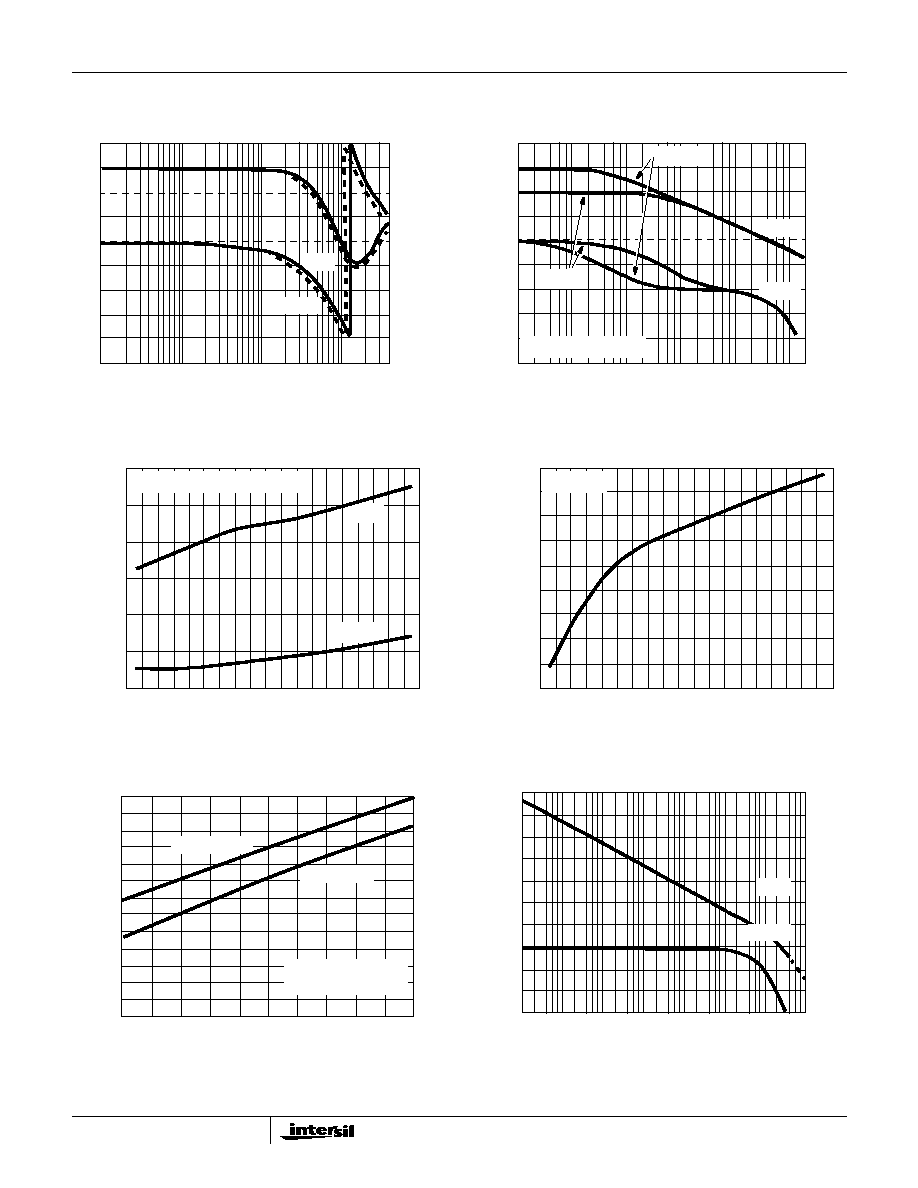
FIGURE 15. CLOSED LOOP FREQUENCY RESPONSE
FIGURE 16. CLOSED LOOP GAIN/PHASE vs FREQUENCY
FIGURE 17. MAXIMUM OUTPUT VOLTAGE vs TEMPERATURE
FIGURE 18. SUPPLY CURRENT vs TEMPERATURE
FIGURE 19. OVERSHOOT vs C
LOAD
FIGURE 20. OPEN LOOP GAIN AND PHASE vs FREQUENCY
Typical Performance Curves
(Continued)
FREQUENCY (Hz)
100K
3
GAIN (dB)
10K
1M
-3
0
10M
-55
o
C
125
o
C
0
90
180
PHASE (DEGREES)
-55
o
C
125
o
C
A
V
= 100
FREQUENCY (Hz)
100K
60
GAIN (dB)
100
1M
0
40
10M
0
90
180
PHASE (DEGREES)
GAIN
PHASE
10K
1K
20
A
V
= 1000
T
A
= 25
o
C, V
S
=
±
15V
R
LOAD
= 2K, A
V
= 1000, V
IN
=
±
2V
TEMPERATURE (
o
C)
0
20
40
60
80
120
13.9
14.0
14.1
V
OUT
MAXIMUM (V)
100
-20
-40
-60
14.5
14.2
14.3
14.4
-V
OUT
+V
OUT
V
S
=
±
15V
TEMPERATURE (
o
C)
0
20
40
60
80
120
4.30
4.40
4.50
SUPPL
Y CURRENT (mA)
100
-20
-40
-60
4.90
4.60
4.70
4.80
5.00
5.10
5.20
LOAD CAPACITANCE (nF)
1.6
40
O
VERSHOO
T (%)
1
1.8
34
38
2
FALLING EDGE
1.4
1.2
36
T
A
= 25
o
C, V
S
=
±
15V
A
V
= 1, V
OUT
= 200mV
RISING EDGE
32
30
28
26
24
22
20
18
16
14
FREQUENCY (Hz)
100K
80
GAIN (dB)
10
1M
0
40
10M
0
90
180
PHASE SHIFT (DEGREES)
GAIN
PHASE
10K
1K
20
45
135
100M
100
60
100
120
HA-5134

9
All Intersil semiconductor products are manufactured, assembled and tested under ISO9000 quality systems certification.
Intersil semiconductor products are sold by description only. Intersil Corporation reserves the right to make changes in circuit design and/or specifications at any time with-
out notice. Accordingly, the reader is cautioned to verify that data sheets are current before placing orders. Information furnished by Intersil is believed to be accurate and
reliable. However, no responsibility is assumed by Intersil or its subsidiaries for its use; nor for any infringements of patents or other rights of third parties which may result
from its use. No license is granted by implication or otherwise under any patent or patent rights of Intersil or its subsidiaries.
For information regarding Intersil Corporation and its products, see web site www.intersil.com
Sales Office Headquarters
NORTH AMERICA
Intersil Corporation
P. O. Box 883, Mail Stop 53-204
Melbourne, FL 32902
TEL: (321) 724-7000
FAX: (321) 724-7240
EUROPE
Intersil SA
Mercure Center
100, Rue de la Fusee
1130 Brussels, Belgium
TEL: (32) 2.724.2111
FAX: (32) 2.724.22.05
ASIA
Intersil (Taiwan) Ltd.
7F-6, No. 101 Fu Hsing North Road
Taipei, Taiwan
Republic of China
TEL: (886) 2 2716 9310
FAX: (886) 2 2715 3029
HA-5134