7-3
CAUTION: These devices are sensitive to electrostatic discharge; follow proper IC Handling Procedures.
http://www.intersil.com or 407-727-9207
|
Copyright
©
Intersil Corporation 1999
HA5320/883
High Speed Precision Sample and Hold Amplifier
Description
The HA-5320/883 was designed for use in precision, high speed
data acquisition systems.
The circuit consists of an input transconductance amplifier
capable of providing large amounts of charging current, a low
leakage analog switch, and an output integrating amplifier. The
analog switch sees virtual ground as its load; therefore, charge
injection on the hold capacitor is constant over the entire input/
output voltage range. The pedestal voltage resulting from this
charge injection can be adjusted to zero by use of the offset
adjust inputs. The device includes a hold capacitor. However, if
improved droop rate is required at the expense of acquisition
time, additional hold capacitance may be added externally.
This monolithic device is manufactured using the Intersil
Dielectric Isolation Process, minimizing stray capacitance and
eliminating SCR's. This allows higher speed and latch-free
operation. For further information, please see Application Note
AN538.
Features
∑ This Circuit is Processed in Accordance to MIL-STD-
883 and is Fully Conformant Under the Provisions of
Paragraph 1.2.1.
∑ Gain, DC . . . . . . . . . . . . . . . . . . . . . . . . 2 x 10
6
V/V (Typ)
∑ Acquisition Time . . . . . . . . . . . . . . . 1.0
µ
s (0.01%) (Typ)
∑ Droop Rate . . . . . . . . . . . . . . . . 0.08
µ
V/
µ
s (+25
o
C) (Typ)
17
µ
V/
µ
s (Full Temperature) (Typ)
∑ Aperture Time. . . . . . . . . . . . . . . . . . . . . . . . . 25ns (Typ)
∑ Hold Step Error . . . . . . . . . . . . . . . . . . . . . . 1.0mV (Typ)
∑ Internal Hold Capacitor
∑ Fully Differential Input
∑ TTL Compatible
Applications
∑ High Bandwidth Precision Data Acquisition Systems
∑ Inertial Navigation and Guidance Systems
∑ Ultrasonics
∑ SONAR / RADAR
∑ Digital to Analog Converter Deglitcher
July 1994
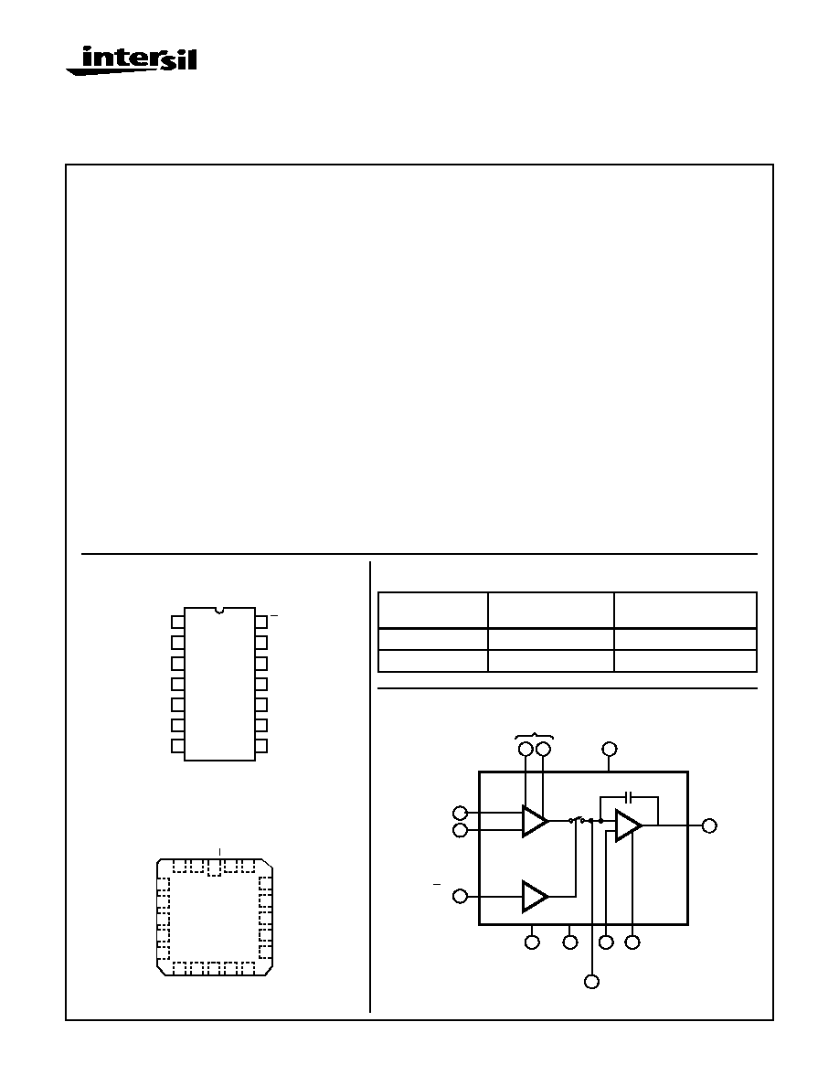
Pinouts
HA-5320/883 (CERDIP)
TOP VIEW
HA-5320/883 (CLCC)
TOP VIEW
-INPUT
+INPUT
V-
SIG GND
OUTPUT
SUPPLY GND
NC
NC
V+
INT. BW
S/H CONTROL
C
EXT
1
2
3
4
5
6
7
14
13
12
11
10
9
8
OFFSET ADJ
OFFSET ADJ
4
5
6
7
8
9
10 11 12 13
3
2
1
20 19
15
14
18
17
16
OFFSET ADJ
NC
OFFSET ADJ
NC
V-
NC
NC
NC
NC
C
EXT
CNTL
S/H
SUPPL
Y GND
NC
SIG
OUTPUT
NC
V+
GND
-I
N
+I
N
INT
. BW
Functional Diagram
Ordering Information
PART NUMBER
TEMPERATURE
RANGE
PACKAGE
HA1-5320/883
-55
o
C to +125
o
C
14 Lead CerDIP
HA4-5320/883
-55
o
C to +125
o
C
20 Lead Ceramic LCC
9
100pF
7
OFFSET
ADJUST
3
4
V+
OUTPUT
HA-5320/883
-INPUT
+INPUT
1
2
CONTROL
S/H
SUPPLY
GND
V-
C
EXT
SIG
GND
INTEGRATOR
BANDWIDTH
14
13
5
8
6
-
+
11
Spec Number
511096-883
File Number
2927.3

7-4
Specifications HA-5320/883
Absolute Maximum Ratings
Thermal Information
Voltage Between V+ and V- Terminals . . . . . . . . . . . . . . . . . . . . 40V
Differential Input Voltage . . . . . . . . . . . . . . . . . . . . . . . . . . . . . . 24V
Digital Input Voltage (S/H Pin) . . . . . . . . . . . . . . . . . . . . . .+8V, -15V
Output Current, Continuous (Note 1)
. . . . . . . . . . . . . . . . . . . . .±
20mA
Storage Temperature Range . . . . . . . . . . . . . . . . . -65
o
C to +150
o
C
Junction Temperature . . . . . . . . . . . . . . . . . . . . . . . . . . . . . . +175
o
C
Lead Temperature (Soldering 10s) . . . . . . . . . . . . . . . . . . . . +300
o
C
ESD Classification . . . . . . . . . . . . . . . . . . . . . . . . . . . . . . . . <2000V
Thermal Resistance
JA
JC
CerDIP Package . . . . . . . . . . . . . . . . . . .
66
o
C/W
16
o
C/W
Ceramic LCC Package . . . . . . . . . . . . . .
57
o
C/W
9
o
C/W
Package Power Dissipation at +75
o
C
CerDip Package . . . . . . . . . . . . . . . . . . . . . . . . . . . . . . . . . . 1.5W
Ceramic LCC Package . . . . . . . . . . . . . . . . . . . . . . . . . . . . 1.75W
Package Power Dissipation Derating Factor Above +75
o
C
CerDip Package . . . . . . . . . . . . . . . . . . . . . . . . . . . . . . 15mW/
o
C
Ceramic LCC Package . . . . . . . . . . . . . . . . . . . . . . . . . 17mW/
o
C
CAUTION: Stresses above those listed in "Absolute Maximum Ratings" may cause permanent damage to the device. This is a stress only rating and operation
of the device at these or any other conditions above those indicated in the operational sections of this specification is not implied.
Operating Conditions
Operating Temperature Range . . . . . . . . . . . . . -55
o
C
T
A
+125
o
C
Operating Supply Voltage (
±
V
S
)
. . . . . . . . . . . . . . . . . . . . . . . . . . ±
15V
Analog Input Voltage
. . . . . . . . . . . . . . . . . . . . . . . . . . . . . . . . . . . . ±
10V
Logic Level Low (V
IL
) . . . . . . . . . . . . . . . . . . . . . . . . . . . . 0V to 0.8V
Logic Level High (V
IH
) . . . . . . . . . . . . . . . . . . . . . . . . . . 2.0V to 5.0V
TABLE 1. DC ELECTRICAL PERFORMANCE CHARACTERISTICS
Device Tested at: V+ = +15V; V- = -15V; V
IL
= 0.8V (Sample); V
IH
= 2.0V (Hold); C
H
= Internal = 100pF; Signal GND = Supply GND,
Unless Otherwise Specified
PARAMETERS
SYMBOL
CONDITIONS
GROUP A
SUBGROUP
TEMPERATURE
LIMITS
UNITS
MIN
MAX
Input Offset Voltage
V
IO
1
+25
o
C
-
1
+
1
mV
2, 3
+125
o
C, -55
o
C
-
2
+
2
mV
Input Bias Current
+I
B
1
+25
o
C
-
200
+
200
nA
2, 3
+125
o
C, -55
o
C
-
200
+
200
nA
-I
B
1
+25
o
C
-
200
+
200
nA
2, 3
+125
o
C, -55
o
C
-
200
+
200
nA
Input Offset Current
I
IO
1
+25
o
C
-
100
+
100
nA
2, 3
+125
o
C, -55
o
C
-
100
+
100
nA
Open Loop Voltage Gain
+A
VS
R
L
= 1k
, V
OUT
= +10V
1
+25
o
C
120
-
dB
2, 3
+125
o
C, -55
o
C
110
-
dB
-A
VS
R
L
= 1k
, V
OUT
= -10V
1
+25
o
C
120
-
dB
2, 3
+125
o
C, -55
o
C
110
-
dB
Common Mode
Rejection Ratio
+CMRR
V+ = 10V, V- = -20V,
V
OUT
= -5V, V
S/H
= -4.2V,
V
GND
= -5V
1
+25
o
C
80
-
dB
2, 3
+125
o
C, -55
o
C
80
-
dB
-CMRR
V+ = 20V, V- = -10V,
V
OUT
= +5V, V
S/H
= 5.8V,
V
GND
= +5V
1
+25
o
C
80
-
dB
2, 3
+125
o
C, -55
o
C
80
-
dB
Output Current
+I
O
V
OUT
= +10V
1
+25
o
C
10
-
mA
2, 3
+125
o
C, -55
o
C
10
-
mA
-I
O
V
OUT
= -10V
1
+25
o
C
-10
-
mA
2, 3
+125
o
C, -55
o
C
-10
-
mA
CAUTION: These devices are sensitive to electronic discharge. Proper IC handling procedures should be followed.
Spec Number
511096-883

7-5
Specifications HA-5320/883
Output Voltage Swing
+V
OP
R
L
= 1k
1
+25
o
C
10
-
V
2, 3
+125
o
C, -55
o
C
10
-
V
-V
OP
R
L
= 1k
1
+25
o
C
-
-10
V
2, 3
+125
o
C, -55
o
C
-
-10
V
Power Supply Current
+I
CC
V
OUT
= 0V, I
OUT
= 0mA
1
+25
o
C
-
13
mA
2, 3
+125
o
C, -55
o
C
-
13
mA
-I
CC
V
OUT
= 0V, I
OUT
= 0mA
1
+25
o
C
-13
-
mA
2, 3
+125
o
C, -55
o
C
-13
-
mA
Power Supply Rejection
Ratio
+PSRR
V+ = 14.5V, 15.5V
V- = -15V, -15V
1
+25
o
C
80
-
dB
2, 3
+125
o
C, -55
o
C
80
-
dB
-PSRR
V+ = +15V, +15V,
V- = -14.5V, -15.5V
1
+25
o
C
65
-
dB
2, 3
+125
o
C, -55
o
C
65
-
dB
Digital Input Current
I
INL
V
IN
= 0V
1
+25
o
C
-
4
µ
A
2, 3
+125
o
C, -55
o
C
-
10
µ
A
I
INH
V
IN
= 5V
1
+25
o
C
-
0.1
µ
A
2, 3
+125
o
C, -55
o
C
-
0.1
µ
A
Digital Input Voltage
V
IL
1
+25
o
C
-
0.8
V
2, 3
+125
o
C, -55
o
C
-
0.8
V
V
IH
1
+25
o
C
2.0
-
V
2, 3
+125
o
C, -55
o
C
2.0
-
V
Output Voltage Droop
Rate
V
D
V
OUT
= 0V
2
+125
o
C
-
100
µ
V/
µ
s
NOTE:
1. Internal power dissipation may limit output current below 20mA.
TABLE 2. AC ELECTRICAL PERFORMANCE CHARACTERISTICS
Table 2 Intentionally Left Blank. See AC Specifications in Table 3.
TABLE 1. DC ELECTRICAL PERFORMANCE CHARACTERISTICS
(Continued)
Device Tested at: V+ = +15V; V- = -15V; V
IL
= 0.8V (Sample); V
IH
= 2.0V (Hold); C
H
= Internal = 100pF; Signal GND = Supply GND,
Unless Otherwise Specified
PARAMETERS
SYMBOL
CONDITIONS
GROUP A
SUBGROUP
TEMPERATURE
LIMITS
UNITS
MIN
MAX
CAUTION: These devices are sensitive to electronic discharge. Proper IC handling procedures should be followed.
Spec Number
511096-883

7-6
Specifications HA-5320/883
TABLE 3. ELECTRICAL PERFORMANCE CHARACTERISTICS
PARAMETER
SYMBOL
CONDITIONS
NOTES
TEMPERATURE
LIMITS
UNITS
MIN
MAX
Hold Mode Feedthrough
V
HMF
V
IN
= 10V
P-P
, 100kHz
1
+25
o
C
-
3
mV
Hold Step Error
V
ERROR
V
IH
= 3.5V, V
IL
= 0V,
T
RISE
(V
IL
to V
IH
) = 10ns
1
+25
o
C
-11
11
mV
Sample Mode Noise
Voltage
E
N(SAMPLE)
DC to 10MHz, V
S/H
= 0V,
R
LOAD
= 2k
1
+25
o
C
-
200
µ
V
RMS
Hold Mode Noise
Voltage
E
N(HOLD)
DC to 10MHz, V
S/H
= 5V,
R
LOAD
= 2k
1
+25
o
C
-
200
µ
V
RMS
Input Capacitance
C
IN
V
S/H
= 0V
1
+25
o
C
-
5
pF
Input Resistance
R
IN
V
S/H
= 0V, Delta V
IN
= 20V
1
+25
o
C
1
-
M
Slew Rate
+SR
C
L
= 50pF, R
L
= 2k
,
V
OUT
= -5V to +5V Step
10%, 90% pts
1
+25
o
C
30
-
V/
µ
s
-SR
C
L
= 50pF, R
L
= 2k
,
V
OUT
= +5V to -5V Step
10%, 90% pts
1
+25
o
C
30
-
V/
µ
s
Rise and Fall Times
T
R
C
L
= 50pF, R
L
= 2k
,
V
OUT
= 0V to +200mV Step
10%, 90% pts
1
+25
o
C
-
150
ns
T
F
C
L
= 50pF, R
L
= 2k
,
V
OUT
= 0V to -200mV Step
10%, 90% pts
1
+25
o
C
-
150
ns
Overshoot
+OS
C
L
= 50pF, R
L
= 2k
,
V
OUT
= 0V to +200mV Step
1
+25
o
C
-
25
%
-OS
C
L
= 50pF, R
L
= 2k
,
V
OUT
= 0V to -200mV Step
1
+25
o
C
-
25
%
0.1% Acquisition Time
T
ACQ
0.1%
C
L
= 50pF, R
L
= 2k
,
V
OUT
= 0V to 10V Step
1
+25
o
C
-
1.2
µ
s
NOTE:
1. The parameters listed in this table are controlled via design or process parameters and are not directly tested. These parameters are
characterized upon initial design release and upon design changes which would affect these characteristics.
TABLE 4. ELECTRICAL TEST REQUIREMENTS
MIL-STD-883 TEST REQUIREMENTS
SUBGROUPS (SEE TABLE 1)
Interim Electrical Parameters (Pre Burn-In)
-
Final Electrical Test Parameters
1(Note 1), 2, 3
Group A Test Requirements
1, 2, 3
Groups C and D Endpoints
1
NOTE:
1. PDA applies to Subgroup 1 only. No other subgroups are included in PDA.
Spec Number
511096-883
7-7
HA-5320/883
Die Characteristics
DIE DIMENSIONS:
92 x 152 x 19
±
1mils
METALLIZATION:
Type: Al, 1% Cu
Thickness: 16k
≈
±
2k
≈
GLASSIVATION:
Type: Nitride (Si
3
N
4
) over Silox (SiO
2
, 5% Phos)
Silox Thickness: 12k
≈
±
2k
≈
Nitride Thickness: 3.5k
≈
±
1.5k
≈
WORST CASE CURRENT DENSITY:
1.742 x 10
5
A/cm
2
TRANSISTOR COUNT: 184
SUBSTRATE POTENTIAL: V-
Metallization Mask Layout
HA-5320/883
C
EXT
V+
(8) INT BW
(7) OUTPUT
(6) SIG GND
V-
V
IO
ADJ
V
IO
ADJ
+INPUT (2)
-INPUT (1)
S/H CTRL (14)
SUPPLY GND
(9)
(11)
(13)
(5)
(4)
(3)
Spec Number
511096-883

7-8
HA-5320/883
Burn-In Circuits
HA-5320/883 DIP BURN-IN/LIFE TEST CIRCUIT
HA-5320/883 LCC BURN-IN/LIFE TEST CIRCUIT
NOTES:
1. R
1
= 100k
, 5%, (per socket).
2. C
1
, C
2
= 0.01
µ
F minimum per socket or 0.1
µ
F minimum per row.
3. D
1
, D
2
= 1N4002 or equivalent (per board).
4. +V = +15.5V
±
0.5V, -V = -15.5V
±
0.5V.
1
2
3
4
5
6
7
14
13
12
11
10
9
8
R
1
-V
D
2
C
2
+V
D
1
C
1
4
5
6
7
8
9
10
11
12
13
3
2
1
20
19
15
14
18
17
16
R
1
-V
D
2
C
2
+V
D
1
C
1
Spec Number
511096-883
7-9
HA-5320/883
F14.3
MIL-STD-1835 GDIP1-T14 (D-1, CONFIGURATION A)
14 LEAD DUAL-IN-LINE FRIT-SEAL CERAMIC PACKAGE
SYMBOL
INCHES
MILLIMETERS
NOTES
MIN
MAX
MIN
MAX
A
-
0.200
-
5.08
-
b
0.014
0.026
0.36
0.66
2
b1
0.014
0.023
0.36
0.58
3
b2
0.045
0.065
1.14
1.65
-
b3
0.023
0.045
0.58
1.14
4
c
0.008
0.018
0.20
0.46
2
c1
0.008
0.015
0.20
0.38
3
D
-
0.785
-
19.94
5
E
0.220
0.310
5.59
7.87
5
e
0.100 BSC
2.54 BSC
-
eA
0.300 BSC
7.62 BSC
-
eA/2
0.150 BSC
3.81 BSC
-
L
0.125
0.200
3.18
5.08
-
Q
0.015
0.060
0.38
1.52
6
S1
0.005
-
0.13
-
7
S2
0.005
-
0.13
-
-
90
o
105
o
90
o
105
o
-
aaa
-
0.015
-
0.38
-
bbb
-
0.030
-
0.76
-
ccc
-
0.010
-
0.25
-
M
-
0.0015
-
0.038
2
N
14
14
8
Packaging
NOTES:
1. Index area: A notch or a pin one identification mark shall be locat-
ed adjacent to pin one and shall be located within the shaded
area shown. The manufacturer's identification shall not be used
as a pin one identification mark.
2. The maximum limits of lead dimensions b and c or M shall be
measured at the centroid of the finished lead surfaces, when
solder dip or tin plate lead finish is applied.
3. Dimensions b1 and c1 apply to lead base metal only. Dimension
M applies to lead plating and finish thickness.
4. Corner leads (1, N, N/2, and N/2+1) may be configured with a
partial lead paddle. For this configuration dimension b3 replaces
dimension b1.
5. This dimension allows for off-center lid, meniscus, and glass
overrun.
6. Dimension Q shall be measured from the seating plane to the
base plane.
7. Measure dimension S1 at all four corners.
8. N is the maximum number of terminal positions.
9. Dimensioning and tolerancing per ANSI Y14.5M - 1982.
10. Controlling Dimension: Inch.
11. Materials: Compliant to MIL-I-38535.
bbb
C A - B
S
c
Q
L
A
SEATING
BASE
D
PLANE
PLANE
-D-
-A-
-C-
-B-
D
E
S1
b2
b
A
e
M
c1
b1
(c)
(b)
SECTION A-A
BASE
LEAD FINISH
METAL
e
A/2
A
M
S
S
e
A
ccc
C A - B
M
D
S
S
aaa
C A - B
M
D
S
S
Spec Number
511096-883

7-10
HA-5320/883
Packaging
(Continued)
D
j x 45
o
D3
B
h x 45
o
A
A1
E
L
L3
e
B3
B1
L1
D2
D1
e
1
E2
E1
L2
PLANE 2
PLANE 1
E3
B2
NOTES:
1. Metallized castellations shall be connected to plane 1 terminals
and extend toward plane 2 across at least two layers of ceramic
or completely across all of the ceramic layers to make electrical
connection with the optional plane 2 terminals.
2. Unless otherwise specified, a minimum clearance of 0.015 inch
(0.381mm) shall be maintained between all metallized features
(e.g., lid, castellations, terminals, thermal pads, etc.)
3. Symbol "N" is the maximum number of terminals. Symbols "ND"
and "NE" are the number of terminals along the sides of length
"D" and "E", respectively.
4. The required plane 1 terminals and optional plane 2 terminals
shall be ellectrically connected.
5. The corner shape (square, notch, radius, etc.) may vary at the
manufacturer's option, from that shown on the drawing.
6. Chip carriers shall be constructed of a minimum of two ceramic
layers.
7. Maximum limits allows for 0.007 inch solder thickness on pads.
8. Materials: Compliant to MIL-I-38535.
J20.A
MIL-STD-1835 CQCC1-N20 (C-2)
20 PAD METAL SEAL LEADLESS CERAMIC CHIP CARRIER
SYMBOL
INCHES
MILLIMETERS
NOTES
MIN
MAX
MIN
MAX
A
0.060
0.100
1.52
2.54
6, 7
A1
0.050
0.088
1.27
2.23
7
B
-
-
-
-
4
B1
0.022
0.028
0.56
0.71
2, 4
B2
0.072 REF
1.83 REF
-
B3
0.006
0.022
0.15
0.56
-
D
0.342
0.358
8.69
9.09
-
D1
0.200 BSC
5.08 BSC
-
D2
0.100 BSC
2.54 BSC
-
D3
-
0.358
-
9.09
2
E
0.342
0.358
8.69
9.09
-
E1
0.200 BSC
5.08 BSC
-
E2
0.100 BSC
2.54 BSC
-
E3
-
0.358
-
9.09
2
e
0.050 BSC
1.27 BSC
-
e1
0.015
-
0.38
-
2
h
0.040 REF
1.02 REF
5
j
0.020 REF
0.51 REF
5
L
0.045
0.055
1.14
1.40
-
L1
0.045
0.055
1.14
1.40
-
L2
0.075
0.095
1.91
2.41
-
L3
0.003
0.015
0.08
0.38
-
ND
5
5
3
NE
5
5
3
N
20
20
3
Spec Number
511096-883
The information contained in this section has been developed through characterization by Intersil Semiconductor and is for use as applica-
tion and design information only. No guarantee is implied.
DESIGN INFORMATION
August 1999
7-11
Semiconductor
HA5320
High Speed Precision
Sample and Hold Amplifier
Applying the HA-5320
The HA-5320 has the uncommitted differential inputs of an
op amp, allowing the Sample and Hold function to be
combined with many conventional op amp circuits. See the
Intersil Application Note 517 for a collection of circuit ideas.
Layout
A printed circuit board with ground plane is recommended
for best performance. Bypass capacitors (0.01 to 0.1
µ
F,
ceramic) should be provided from each power supply termi-
nal to the Supply Ground terminal on pin 13.
The ideal ground connections are pin 6 (SIG. Ground)
directly to the system Signal Ground, and pin 13 (Supply
Ground) directly to the system Supply Common.
Hold Capacitor
The HA-5320 includes a 100pF MOS hold capacitor, suffi-
cient for most high speed applications (the Electrical Specifi-
cations section is based on this internal capacitor).
Additional capacitance may be added between pins 7 and
11. This external hold capacitance will reduce droop rate at
the expense of acquisition time, and provide other trade-offs
as shown in the Performance Curves.
If an external hold capacitor C
EXT
is used, then a noise
band- width capacitor of value 0.1C
EXT
should be connected
from pin 8 to ground. Exact value and type are not critical.
The hold capacitor C
EXT
should have high insulation resis-
tance and low dielectric absorption, to minimize droop
errors. Polystyrene dielectric is a good choice for operating
temperatures up to +85
o
C. Teflon
Æ
and glass dielectrics
offer good performance to +125
o
C and above.
The hold capacitor terminal (pin 11) remains at virtual
ground potential. Any PC connection to this terminal should
be kept short and "guarded" by the ground plane, since
nearby signal lines or power supply voltages will introduce
errors due to drift current.
Æ
Teflon is a registered Trademark of Dupont Corporation.
Applications
Figure 1 shows the HA-5320 connected as a unity gain non-
inverting amplifier ≠ its most widely used configuration. As
an input device for a fast successive ≠ approximation A/D
converter, it offers very high throughput rate for a monolithic
IC sample/hold amplifier. Also, the hold step error is adjust-
able to zero using the Offset Adjust potentiometer, to deliver
a 12-bit accurate output from the converter.
The application may call for an external hold capacitor C
EXT
as shown. As mentioned earlier, 0.1C
EXT
is then recom-
mended at pin 8 to reduce output noise in the Hold mode.
The HA-5320 output circuit does not include short circuit
protection, and consequently its output impedance remains
low at high frequencies. Thus, the step changes in load cur-
rent which occur during an A/D conversion are absorbed at
the S/H output with minimum voltage error. A momentary
short circuit to ground is permissible, but the output is not
designed to tolerate a short of indefinite duration.
FIGURE 1. TYPICAL HA-5320/883 CONNECTIONS; NONINVERTING UNITY GAIN MODE
NOTE: Pin Numbers Refer to DIP Package Only.
100pF
DIGITAL
OUTPUT
C
EXT
HA-5320
0.1C
EXT
V
IN
H
S
S/H CONTROL
7
13
11
9
5
4
3
-15V +15V
10k
OFFSET
ADJUST
±
15mV
1
2
14
13
6
8
SYSTEM
SIGNAL
GROUND
SYSTEM
POWER
GROUND
CONVERT
5
9
ANALOG
COMMON
R/C
INPUT
HI-574A
-
+
-
+
Spec Number
511096-883

DESIGN INFORMATION
(Continued)
The information contained in this section has been developed through characterization by Intersil Semiconductor and is for use as applica-
tion and design information only. No guarantee is implied.
7-12
HA-5320
Test Circuits
CHARGE TRANSFER AND DRIFT CURRENT
CHARGE TRANSFER TEST
1. Observe the "hold step" voltage V
p
:
2. Compute charge transfer: Q = V
p
C
H
DRIFT CURRENT TEST
1. Observe the voltage "droop",
V
O
/
T:
2. Measure the slope of the output during hold,
V
O
/
T, and com-
pute drift current: I
D
= C
H
V
O
/
T.
HOLD MODE FEED THROUGH ATTENUATION
Feedthrough in dB = 20 Log
V
OUT
where:
V
IN
V
OUT
= Volts
p-p
, Hold Mode,
V
IN
= Volts
p-p
.
14
2
1
7
11
N.C.
-INPUT
+INPUT
S/H CONTROL
CONTROL
INPUT
S/H
OUTPUT
V
O
(C
H
= 100pF)
HA-5320
8
N.C.
HOLD (+3.5V)
SAMPLE (0V)
S/H CONTROL
V
O
V
p
V
O
T
S/H CONTROL
V
O
HOLD (4.0V)
SAMPLE (0V)
V
IN
ANALOG
MUX OR
SWITCH
A
IN
S/H CONTROL
C
EXT
REF
COM
SUPPLY
GND
+IN
-IN
TO
SIGNAL
GND
TO
SUPPLY
COMMON
N.C.
OUT
V
OUT
7
13
11
6
1
2
14
-V
+V
S/H CONTROL
INPUT
9
5
HA-5320
100kHz
SINE WAVE
10V
p-p
INT.
COMP.
N.C.
8
Spec Number
511096-883

DESIGN INFORMATION
(Continued)
The information contained in this section has been developed through characterization by Intersil Semiconductor and is for use as applica-
tion and design information only. No guarantee is implied.
7-13
HA-5320
Performance Curves
V
SUPPLY
=
±
15VDC
TYPICAL SAMPLE AND HOLD PERFORMANCE
AS FUNCTION OF HOLDING CAPACITOR
DRIFT CURRENT vs TEMPERATURE
OPEN LOOP GAIN AND PHASE RESPONSE
TYPICAL SAMPLE-TO-HOLD OFFSET (HOLD STEP) ERROR
HOLD STEP vs. INPUT VOLTAGE
HOLD STEP vs. LOGIC (V
IH
) VOLTAGE
10
5
1.0
0.5
0.1
0.05
0.01
100
1000
10K
100K
CH VALUE (pF)
ACQUISITION TIME
FOR 10V STEP TO +0.01%(
µ
s)
VOLTAGE DROOP
DURING HOLD MODE
(mV/100ms)
SAMPLE-TO-HOLD
OFFSET (HOLD STEP)
ERROR (mV)
1.0
10
100
1000
I
DRIFT
(pA)
TEMPERATURE (
o
C)
-25
0
+25 +50 +75 +100 +125
C
H
= 100pF, INTERNAL
120
100
80
60
40
20
0
GAIN (dB)
PHASE (DEGREES)
0
45
90
135
180
10
100
1K
10K
100K
1M
10M
FREQUENCY (Hz)
G
G
(C
H
= 1100pF)
(C
H
= 100pF)
HOLD STEP
VOLTAGE
(mV)
-10
-8
-6
-4
-2
2
10
8
6
4
T
A
= +25
o
C
C
H
= 100pF
C
H
= 1000pF
C
H
= 0.01
µ
F
1.0
0.1
0.01
DC INPUT (V)
LOGIC LEVEL HIGH (V)
2
3
4
5
2.0
1.5
1.0
0.5
0.0
HOLD STEP VOL
T
AGE (mV)
+25
o
C
+75
o
C
C
H
= 100pF
Spec Number
511096-883

DESIGN INFORMATION
(Continued)
The information contained in this section has been developed through characterization by Intersil Semiconductor and is for use as applica-
tion and design information only. No guarantee is implied.
7-14
HA-5320
Acquisition Time
The time required following a "sample" command, for the
output to reach its final value within
±
0.1% or
±
0.01%. This is
the minimum sample time required to obtain a given accu-
racy, and includes switch delay time, slewing time and set-
tling time.
Charge Transfer
The small charge transferred to the holding capacitor from
the inter-electrode capacitance of the switch when the unit is
switched to the HOLD mode. Charge transfer is directly pro-
portional to sample-to-hold offset pedestal error, where:
Charge Transfer (pC) = C
H
(pF) x Offset Error (V)
Aperture Time
The time required for the sample-and-hold switch to open,
independent of delays through the switch driver and input
amplifier circuitry. The switch opening time is the interval
between the conditions of 10% open and 90% open.
Hold Step Error
Hold Step Error is the output error due to Charge Transfer
(see above). It may be calculated from Charge Transfer,
using the following relationship:
HOLD STEP (V) =
CHARGE TRANSFER (pC)
HOLD CAPACITANCE (pF)
See Performance Curves.
Effective Aperture Delay Time (EADT)
The difference between propagation time from the analog
input to S/H switch, and digital delay time between the Hold
command and opening of the switch.
EADT may be positive, negative or zero. If zero, the S/H
amplifier will output a voltage equal to V
IN
at the instant the
Hold command was received. For negative EADT, the output
in Hold (exclusive of pedestal and droop errors) will
correspond to a value of V
IN
that occurred before the Hold
command.
Aperture Uncertainty
The range of variation in Effective Aperture Delay Time.
Aperture Uncertainty (also called Aperture Delay
Uncertainty, Aperture Time Jitter, etc.) sets a limit on the
accuracy with which a waveform can be reconstructed from
sample data.
Drift Current
The net leakage current from the hold capacitor during the
hold mode. Drift current can be calculated from the droop
rate using the formula:
I
D
(pA) = C
H
(pF) x
V
(V/s)
T
Glossary of Terms
TYPICAL PERFORMANCE CHARACTERISTICS
PARAMETER
CONDITIONS
TEMPERATURE
TYP
UNITS
Input Voltage Range
Full
±
10
V
Offset Voltage Drift
Full
5
µ
V/
o
C
Gain Bandwidth Product (C
H
= 100pF)
Av = +1, V
O
= 200mV
P-P
, R
L
= 2K, C
L
= 50pF
+25
o
C
2
MHz
Gain Bandwidth Product (C
H
= 1000pF)
Av = +1, V
O
= 200mV
P-P
, R
L
= 2K, C
L
= 50pF
+25
o
C
0.18
MHz
Full Power Bandwidth
V
O
= 20V
P-P
, R
L
= 2K, C
L
= 50pF
+25
o
C
600
kHz
Output Resistance (Hold Mode)
+25
o
C
1.0
0.1% Acquisition Time
V
O
= 10V Step, R
L
= 2K, C
L
= 50pF
+25
o
C
0.8
µ
s
0.01% Acquisition Time
V
O
= 10V Step, R
L
= 2K, C
L
= 50pF
+25
o
C
1.0
µ
s
Effective Aperture Delay Time
+25
o
C
-25
ns
Aperture Uncertainty
+25
o
C
0.3
ns
0.01% Hold Mode Settling Time
+25
o
C
165
ns
Spec Number
511096-883
All Intersil semiconductor products are manufactured, assembled and tested under ISO9000 quality systems certification.
Intersil products are sold by description only. Intersil Corporation reserves the right to make changes in circuit design and/or specifications at any time without
notice. Accordingly, the reader is cautioned to verify that data sheets are current before placing orders. Information furnished by Intersil is believed to be accurate
and reliable. However, no responsibility is assumed by Intersil or its subsidiaries for its use; nor for any infringements of patents or other rights of third parties which
may result from its use. No license is granted by implication or otherwise under any patent or patent rights of Intersil or its subsidiaries.
For information regarding Intersil Corporation and its products, see web site http://www.intersil.com