1
CAUTION: These devices are sensitive to electrostatic discharge; follow proper IC Handling Procedures.
1-888-INTERSIL or 321-724-7143
|
Copyright
©
Intersil Corporation 1999
HA-5330
650ns Precision Sample and Hold
Amplifier
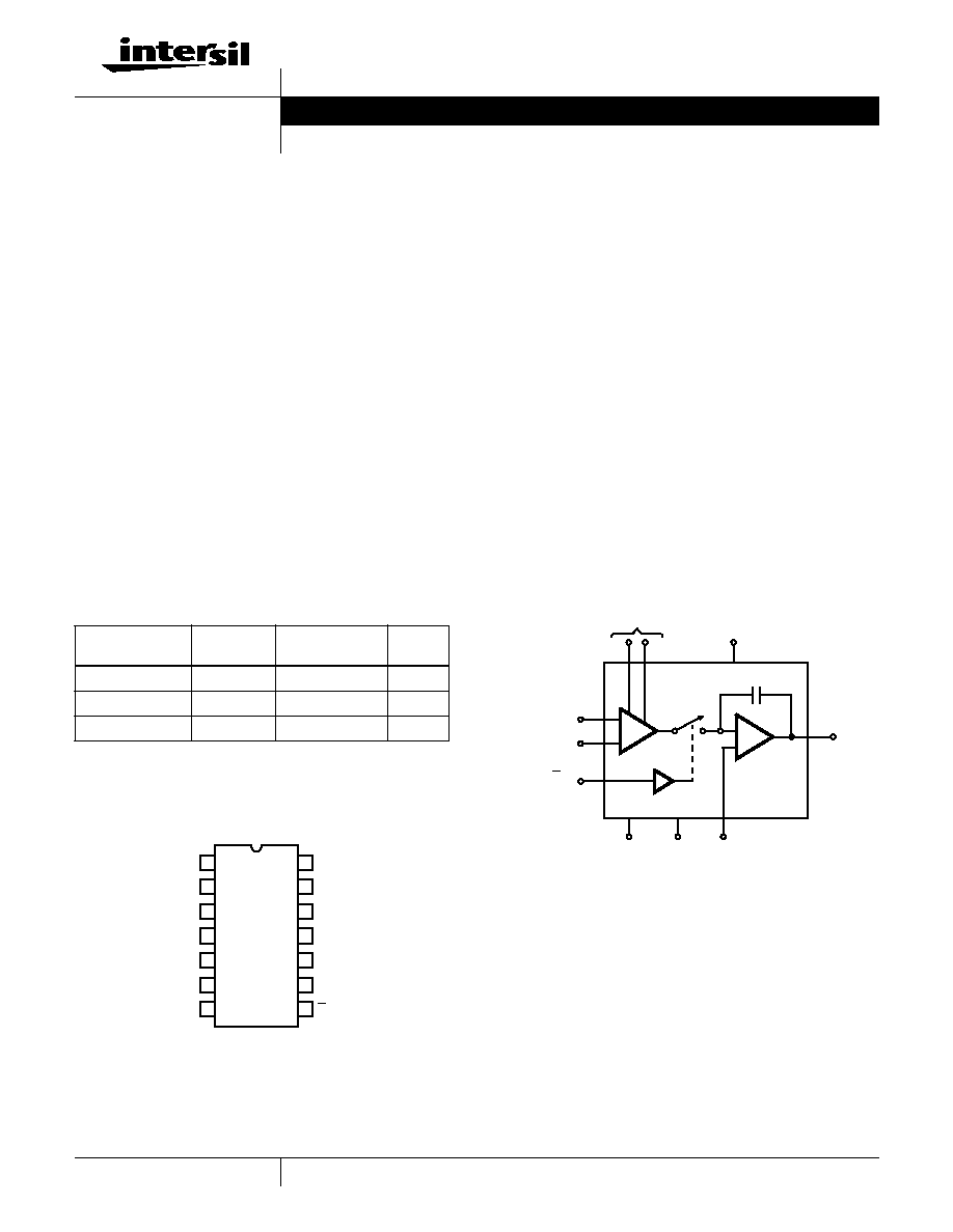
The HA-5330 is a very fast sample and hold amplifier
designed primarily for use with high speed A/D converters. It
utilizes the Intersil Dielectric Isolation process to achieve a
650ns acquisition time to 12-bit accuracy and a droop rate of
0.01
µ
V/
µ
s. The circuit consists of an input transconductance
amplifier capable of producing large amounts of charging
current, a low leakage analog switch, and an integrating
output stage which includes a 90pF hold capacitor.
The analog switch operates into a virtual ground, so charge
injection on the hold capacitor is constant and independent
of V
IN
. Charge injection is held to a low value by
compensation circuits and, if necessary, the resulting 0.5mV
hold step error can be adjusted to zero via the Offset Adjust
terminals. Compensation is also used to minimize leakage
currents which cause voltage droop in the Hold mode.
The HA-5330 will operate at reduced supply voltages (to
±
10V) with a reduced signal range. The MIL-STD-883 data
sheet for this device is available on request.
Pinout
HA-5330
(PDIP, CERDIP)
TOP VIEW
Features
∑ Very Fast Acquisition . . . . . . 500ns (0.1%) 650ns (0.01%)
∑ Low Droop Rate . . . . . . . . . . . . . . . . . . . . . . . . 0.01
µ
V/
µ
s
∑ Very Low Offset . . . . . . . . . . . . . . . . . . . . . . . . . . . 0.2mV
∑ High Slew Rate. . . . . . . . . . . . . . . . . . . . . . . . . . . . 90V/
µ
s
∑ Wide Supply Range
. . . . . . . . . . . . . . . . . . . . . ±
10V to
±
20V
∑ Internal Hold Capacitor
∑ Fully Differential Input
∑ TTL/CMOS Compatible
Applications
∑ Precision Data Acquisition Systems
∑ D/A Converter Deglitching
∑ Auto-Zero Circuits
∑ Peak Detectors
Functional Diagram
Ordering Information
PART NUMBER
TEMP.
RANGE (
o
C)
PACKAGE
PKG.
NO.
HA1-5330-2
-55 to 125
14 Ld CERDIP
F14.3
HA1-5330-5
0 to 75
14 Ld CERDIP
F14.3
HA3-5330-5
0 to 75
14 Ld PDIP
E14.3
+IN
NC
OFFSET ADJ.
OFFSET ADJ.
V-
NC
OUTPUT
-IN
NC
SIGNAL GND
SUPPLY GND
V+
NC
S/H CONTROL
1
2
3
4
5
6
7
14
13
12
11
10
9
8
GND
SUPPLY
V-
SIGNAL
GND
11
5
8
1
14
CONTROL
S/H
+IN
IN
-
HA-5330
7
OUT
12
90pF
OFFSET
ADJUST
4
3
V+
10
Data Sheet
September 1998
File Number
2858.3

2
Absolute Maximum Ratings
Thermal Information
Voltage between V+ and SUPPLY/SIG GND . . . . . . . . . . . . . . +20V
Voltage between V- and SUPPLY/SIG GND . . . . . . . . . . . . . . . -20V
Voltage between SUPPLY GND and SIG GND . . . . . . . . . . . .
±
2.0V
Voltage between S/H Control and SUPPLY/SIG GND . . . . +8V, -6V
Differential Input Voltage . . . . . . . . . . . . . . . . . . . . . . . . . . . . . . 24V
Output Current, Continuous (Note 1) . . . . . . . . . . . . . . . . . . .
±
17mA
Operating Conditions
Temperature Range
HA-5330-2 . . . . . . . . . . . . . . . . . . . . . . . . . . . . . . -55
o
C to 125
o
C
HA-5330-5 . . . . . . . . . . . . . . . . . . . . . . . . . . . . . . . . 0
o
C to 75
o
C
Supply Voltage Range (Typical) . . . . . . . . . . . . . . . . .
±
10V to
±
20V
Thermal Resistance (Typical, Note 3)
JA
(
o
C/W)
JC
(
o
C/W)
CERDIP Package . . . . . . . . . . . . . . . . .
66
16
PDIP Package . . . . . . . . . . . . . . . . . . .
90
N/A
Maximum Junction Temperature (Ceramic Package, Note 2) . . .175
o
C
Maximum Junction Temperature (Plastic Package) . . . . . . . .150
o
C
Maximum Storage Temperature Range . . . . . . . . . . -65
o
C to 150
o
C
Maximum Lead Temperature (Soldering 10s) . . . . . . . . . . . . 300
o
C
CAUTION: Stresses above those listed in "Absolute Maximum Ratings" may cause permanent damage to the device. This is a stress only rating and operation of the
device at these or any other conditions above those indicated in the operational sections of this specification is not implied.
NOTES:
1. Internal Power Dissipation may limit Output Current below
±
17mA.
2. Maximum power dissipation, including output load, must be designed to maintain the junction temperature below 175
o
C for the ceramic package,
and below 150
o
C for the plastic package.
3.
JA
is measured with the component mounted on an evaluation PC board in free air.
Electrical Specifications
V
SUPPLY
=
±
15V; S/H Control V
IL
= +0.8V (Sample): V
IH
= +2.0V (Hold); SIG GND = SUPPLY GND,
Unity Gain Configuration (Output tied to -Input), Unless Otherwise Specified
PARAMETER
TEST
CONDITIONS
TEMP.
(
o
C)
HA-5330-2
HA-5330-5
UNITS
MIN
TYP
MAX
MIN
TYP
MAX
INPUT CHARACTERISTICS
Input Voltage Range
Full
±
10
-
-
±
10
-
-
V
Input Resistance (Note 4)
25
5
15
-
5
15
-
M
Input Capacitance
25
-
3
-
-
3
-
pF
Offset Voltage
25
-
0.2
-
-
0.2
-
mV
Full
-
-
2.0
-
-
1.5
mV
Offset Voltage Temperature Coefficient
Full
-
1
10
-
1
10
µ
V/
o
C
Bias Current
25
-
±
20
-
-
±
20
-
nA
Full
-
-
±
500
-
-
±
300
nA
Offset Current
25
-
20
-
-
20
-
nA
Full
-
-
500
-
-
300
nA
Common Mode Range
Full
±
10
-
-
±
10
-
-
V
CMRR
V
CM
=
±
10V
Full
86
100
-
86
100
-
dB
TRANSFER CHARACTERISTICS
Gain
DC
Full
2 x 10
6
2 x 10
7
-
2 x 10
6
2 x 10
7
-
V/V
Gain Bandwidth Product
Note 12
25
-
4.5
-
-
4.5
-
MHz
OUTPUT CHARACTERISTICS
Output Voltage
Full
±
10
-
-
±
10
-
-
V
Output Current
Full
±
10
-
-
±
10
-
-
mA
Full Power Bandwidth (Note 6)
25
-
1.4
-
-
1.4
-
MHz
Output Resistance
Hold Mode
25
-
0.2
-
-
0.2
-
Sample Mode
25
-
10
-5
0.001
-
10
-5
0.001
HA-5330

3
Total Output Noise, DC to 4MHz
Sample Mode
-
230
-
-
230
-
µ
V
RMS
Hold Mode
25
-
190
-
-
190
-
µ
V
RMS
TRANSIENT RESPONSE
Rise Time
Note 5
25
-
70
-
-
70
-
ns
Overshoot
Note 5
25
-
10
-
-
10
-
%
Slew Rate
Note 7
25
-
90
-
-
90
-
V/
µ
s
DIGITAL INPUT CHARACTERISTICS
Input Voltage
V
IH
Full
2.0
-
-
2.0
-
-
V
V
IL
Full
-
-
0.8
-
-
0.8
V
Input Current
V
IL
= 0V
Full
-
10
40
-
10
40
µ
A
V
IH
= 5V
Full
-
10
40
-
10
40
µ
A
SAMPLE/HOLD CHARACTERISTICS
Acquisition Time
To 0.1%, Note 8
25
-
500
-
-
500
-
ns
Full
-
-
700
-
-
700
ns
To 0.01%, Note 8
25
-
650
-
-
650
-
ns
Full
-
-
900
-
-
900
ns
Aperture Time (Note 4)
25
-
20
-
-
20
-
ns
Effective Aperture Delay Time
25
-50
-25
0
-50
-25
0
ns
Aperture Uncertainty
25
-
0.1
-
-
0.1
-
ns
Droop Rate (Note 9)
25
-
0.01
-
-
0.01
-
µ
V/
µ
s
Full
-
-
100
-
-
10
µ
V/
µ
s
Hold Step Error
Note 10
25
-
0.5
-
-
0.5
-
mV
Hold Mode Settling Time
To 0.01%
25
-
100
200
-
100
200
ns
Hold Mode Feedthrough
20V
P-P
, 100kHz
Full
-
-88
-
-
-88
-
dB
POWER SUPPLY CHARACTERISTICS
Positive Supply Current
Full
-
18
22
-
18
24
mA
Negative Supply Current
Full
-
19
23
-
19
25
mA
Power Supply Rejection
Note 11
Full
86
100
-
86
100
-
dB
NOTES:
4. Derived from computer simulation only; not tested.
5. V
I
= 200mV Step; R
L
= 2k
; C
L
= 50pF.
6. Full power bandwidth based on slew rate measurement using:
. Distortion of wave shape occurs beyond 100kHz due to
slew rate enhancement circuitry.
7. V
O
= 20V Step; R
L
= 2k
; C
L
= 50pF.
8. V
O
= 10V Step; R
L
= 2k
; C
L
= 50pF.
9. This parameter is measured at ambient temperature extremes in a high speed test environment. Consequently, steady state heating effects from
internal power dissipation are not included.
10. V
IN
= 0V; V
IH
= +3.5V; t
R
= 22ns (V
IL
to V
IH
). See graph.
11. Based on a 3V delta in each supply, i.e. 15V
±
1.5V
DC
.
12. V
OUT
= 200mV
P-P
, R
L
= 2k
, C
L
= 50pF.
Electrical Specifications
V
SUPPLY
=
±
15V; S/H Control V
IL
= +0.8V (Sample): V
IH
= +2.0V (Hold); SIG GND = SUPPLY GND,
Unity Gain Configuration (Output tied to -Input), Unless Otherwise Specified (Continued)
PARAMETER
TEST
CONDITIONS
TEMP.
(
o
C)
HA-5330-2
HA-5330-5
UNITS
MIN
TYP
MAX
MIN
TYP
MAX
FPBW
Slew Rate
2
V
PEAK
---------------------------
=
HA-5330
4
Application Information
The HA-5330 has the uncommitted differential inputs of an
op amp, allowing the Sample/Hold function to be combined
with many conventional op amp circuit ideas. See the Intersil
Application Note AN517 for a collection of circuit ideas.
Layout
A printed circuit board with ground plane is recommended
for best performance. Bypass capacitors (0.01
µ
F to 0.1
µ
F,
ceramic) should be provided from each power supply
terminal to the Supply GND Terminal on pin 11.
Typical Applications
The HA-5330 is configured as a unity gain noninverting
amplifier by simply connecting the output (pin 7) to the
inverting input (pin 14). As an input device for a fast
successive - approximation A/D converter, it offers an
extremely high throughput rate. Also, the HA-5330's
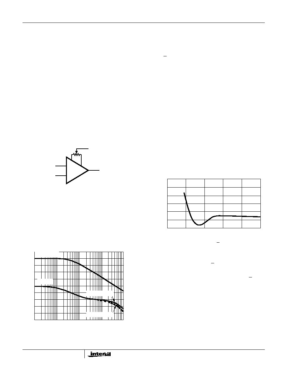
pedestal error is adjustable to zero by using an Offset Adjust
potentiometer (10K to 50K) center tapped to V-.
The ideal ground connections are pin 11 (Supply Ground)
directly to the system Supply Common, and pin 12 (Signal
Ground) directly to the system Signal Ground (Analog
Ground).
Hold Capacitor
The HA-5330 includes a 90pF MOS hold capacitor, sufficient
for most high speed applications (the Electrical
Specifications section is based on the internal capacitor).
Output Stage
The HA-5330 output circuit does not include short circuit
protection, and consequently its output impedance remains
low at high frequencies. Thus, the step changes in load
current which occur during an A/D conversion are absorbed
at the S/H output with minimum voltage error. A momentary
short circuit to ground is permissible, but the output is not
designed to tolerate a short of indefinite duration.
Glossary of Terms
Acquisition Time
The time required following a "sample" command, for the
output to reach its final value within
±
0.1% or
±
0.01%. This is
the minimum sample time required to obtain a given
accuracy, and includes switch delay time, slewing time and
settling time.
Aperture Time
The time required for the sample-and-hold switch to open,
independent of delays through the switch driver and input
amplifier circuitry. The switch opening time is that interval
between the conditions of 10% open and 90% open.
Hold Step Error
Hold step error is the output shift due to charge transfer from
the sample to the hold mode. It is also referred to as "offset
step" or "pedestal error".
Effective Aperture Delay Time (EADT)
The difference between the digital delay time from the Hold
command to the opening of the S/H switch, and the
propagation time from the analog input to the switch.
EADT may be positive, negative or zero. If zero, the S/H
amplifier will output a voltage equal to V
IN
at the instant the
Hold command was received. For negative EADT, the output
in Hold (exclusive of pedestal and droop errors) will
correspond to a value of V
IN
that occurred before the Hold
command.
Aperture Uncertainty
The range of variation in Effective Aperture Delay Time.
Aperture Uncertainty (also called Aperture Delay Uncertainty,
Aperture Time Jitter, etc.) sets a limit on the accuracy with
which a waveform can be reconstructed from sample data.
3
4
10k
- 50k
V-
FIGURE 1. HA-5330 OFFSET ADJUST
40
20
0
-20
-40
MA
GNITUDE (dB)
1K
10K
100K
1M
10M
FREQUENCY (Hz)
MAGNITUDE
PHASE
±
15V SUPPLIES
±
12V SUPPLIES
PHASE (DEGREES)
180
90
0
FIGURE 2. MAGNITUDE AND PHASE RESPONSE
(CLOSED LOOP GAIN = 100)
20
40
60
80
100
3.0
2.0
1.0
0.0
-1.0
-2.0
HOLD STEP ERR
OR (mV)
RISE TIME (ns) 0V TO 3.5V
FIGURE 3. HOLD STEP ERROR vs S/H CONTROL RISE TIME
HA-5330

5
All Intersil semiconductor products are manufactured, assembled and tested under ISO9000 quality systems certification.
Intersil semiconductor products are sold by description only. Intersil Corporation reserves the right to make changes in circuit design and/or specifications at any time with-
out notice. Accordingly, the reader is cautioned to verify that data sheets are current before placing orders. Information furnished by Intersil is believed to be accurate and
reliable. However, no responsibility is assumed by Intersil or its subsidiaries for its use; nor for any infringements of patents or other rights of third parties which may result
from its use. No license is granted by implication or otherwise under any patent or patent rights of Intersil or its subsidiaries.
For information regarding Intersil Corporation and its products, see web site http://www.intersil.com
Die Characteristics
DIE DIMENSIONS:
99 mils x 166 mils x 19 mils
2510
µ
m x 4210
µ
m x 483
µ
m
METALLIZATION:
Type: Al, 1% Cu
Thickness: 16k
≈
±
2k
≈
PASSIVATION:
Type: Nitride (Si
3
N
4
) over Silox (SiO
2
, 5% Phos.)
Silox Thickness: 12k
≈
±
2k
≈
Nitride Thickness: 3.5k
≈
±
1.5k
≈
SUBSTRATE POTENTIAL (Powered Up):
Signal GND
TRANSISTOR COUNT:
205
PROCESS:
Bipolar Dielectric Isolation
Metallization Mask Layout
HA-5330
+IN
-IN
SIGNAL GND
SUPPLY GND
V+
S/H CONTROL
OUTPUT
V-
OFFSET ADJ
OFFSET ADJ
HA-5330