
7-8
CAUTION: These devices are sensitive to electrostatic discharge; follow proper IC Handling Procedures.
http://www.intersil.com or 407-727-9207
|
Copyright
©
Intersil Corporation 1999
HA5340/883
High Speed, Low Distortion, Precision Monolithic
Sample and Hold Amplifier
Description
The HA-5340/883 combines the advantages of two sample/hold
architectures to create a new generation of monolithic sample/
hold. High amplitude, high frequency signals can be sampled
with very low distortion being introduced. The combination of
exceptionally fast acquisition time and specified/characterized
hold mode distortion is an industry first. Additionally, the AC
performance is only minimally affected by additional hold
capacitance.
To achieve this level of performance, the benefits of an
integrating output stage have been combined with the
advantages of a buffered hold capacitor. To the user this
translates to a front-end stage that has high bandwidth due to
charging only a small capacitive load and an output stage with
constant pedestal error which can be nulled out using the offset
adjust pins. Since the performance penalty for additional hold
capacitance is low, the designer can further minimize pedestal
error and droop rate without sacrificing speed.
Low distortion, fast acquisition, and low droop rate are the
result, making the HA-5340/883 the obvious choice for high
speed, high accuracy sampling systems.
Features
∑ This Circuit is Processed in Accordance to MIL-STD-
883 and is Fully Conformant Under the Provisions of
Paragraph 1.2.1.
∑ Fast Acquisition Time (0.01%) . . . . . . . . . . . . . . . 900ns
∑ Fast Hold Mode Settling Time (0.01%) . . . . . . . . . 300ns
∑ Low Distortion (Hold Mode) . . . . . . . . . . . -72dBc (Typ)
(V
IN
= 200kHz, Fs = 450kHz, 5V
P-P
)
∑ Bandwidth Minimally Affected By External C
H
∑ Fully Differential Analog Inputs
∑ Built-in 135pF Hold Capacitor
∑ Pin Compatible with HA-5320
Applications
∑ High Bandwidth Precision Data Acquisition Systems
∑ Inertial Navigation and Guidance Systems
∑ Ultrasonics
∑ SONAR
∑ RADAR
June 1994
Pinouts
HA-5340/883 (CERDIP)
TOP VIEW
HA-5340/883 (CLCC)
TOP VIEW
-INPUT
+INPUT
V-
SIG GND
OUTPUT
SUPPLY GND
NC
NC
V+
NC
S/H CONTROL
EXTERNAL
HOLD CAP
1
2
3
4
5
6
7
14
13
12
11
10
9
8
OFFSET ADJ
OFFSET ADJ
4
5
6
7
8
9
10 11 12 13
3
2
1
20 19
15
14
18
17
16
OFFSET ADJ
NC
OFFSET ADJ
NC
V-
NC
NC
NC
NC
EXT. HOLD CAP.
CNTL
S/H
SUPPL
Y
GND
NC
SIG
OUTPUT
NC
NC
V+
GND
-IN
+IN
Functional Diagram
NOTE: Buffer acts as a buffer in sample mode, acts as a closed switch in hold
mode.
Ordering Information
PART NUMBER
TEMPERATURE
RANGE
PACKAGE
HA1-5340/883
-55
o
C to +125
o
C
14 Lead CerDIP
HA4-5340/883
-55
o
C to +125
o
C
20 Lead Ceramic LCC
4
3
7
OFFSET
ADJUST
+V
7
OUT
6
9
5
13
GND
SUPPL
Y
SIGNAL
GND
C
COMP
15pF
120pF
C
HOLD
14
2
1
CONTROL
S/H
11
(OPTIONAL)
C
HOLD
EXTERNAL
-IN
+IN
-V
*
Spec Number
511117-883
File Number
2452.1

7-9
Specifications HA5340/883
Absolute Maximum Ratings
Thermal Information
Voltage Between V+ and V- Terminals . . . . . . . . . . . . . . . . . . . . 36V
Differential Input Voltage . . . . . . . . . . . . . . . . . . . . . . . . . . . . . . 24V
Digital Input Voltage (S/H Pin) . . . . . . . . . . . . . . . . . . . . . . .+8V, -6V
Output Current, Continuous
. . . . . . . . . . . . . . . . . . . . . . . . . . . . .±
20mA
Storage Temperature Range . . . . . . . . . . . . . . . . . -65
o
C to +150
o
C
Junction Temperature . . . . . . . . . . . . . . . . . . . . . . . . . . . . . . +175
o
C
Lead Temperature (Soldering 10s) . . . . . . . . . . . . . . . . . . . . +300
o
C
ESD Classification . . . . . . . . . . . . . . . . . . . . . . . . . . . . . . . . <2000V
Thermal Resistance
JA
JC
CerDIP Package . . . . . . . . . . . . . . . . .
68
o
C/W
17
o
C/W
Ceramic LCC Package . . . . . . . . . . . .
68
o
C/W
18
o
C/W
Package Power Dissipation at +75
o
C
CerDip Package . . . . . . . . . . . . . . . . . . . . . . . . . . . . . . . . . . 1.5W
Ceramic LCC Package . . . . . . . . . . . . . . . . . . . . . . . . . . . . . 1.5W
Package Power Dissipation Derating Factor Above +75
o
C
CerDip Package . . . . . . . . . . . . . . . . . . . . . . . . . . . . . . 15mW/
o
C
Ceramic LCC Package . . . . . . . . . . . . . . . . . . . . . . . . . 15mW/
o
C
CAUTION: Stresses above those listed in "Absolute Maximum Ratings" may cause permanent damage to the device. This is a stress only rating and operation
of the device at these or any other conditions above those indicated in the operational sections of this specification is not implied.
Operating Conditions
Operating Temperature Range . . . . . . . . . . . . -55
o
C
T
A
+125
o
C
Operating Supply Voltage (
±
V
S
)
. . . . . . . . . . . . . . . . . . . . . . . . . . ±
15V
Analog Input Voltage
. . . . . . . . . . . . . . . . . . . . . . . . . . . . . . . . . . . . ±
10V
Logic Level Low (V
IL
) . . . . . . . . . . . . . . . . . . . . . . . . . . . . 0V to 0.8V
Logic Level High (V
IH
) . . . . . . . . . . . . . . . . . . . . . . . . . . 2.0V to 5.0V
TABLE 1. DC ELECTICAL PERFORMANCE CHARACTERISTICS
Device Tested at: V+ = +15V; V- = -15V; V
IL
= 0.8V (Sample); V
IH
= 2.0V (Hold); C
H
= Internal = 135pF; Signal GND = Supply GND,
Unless Otherwise Specified.
PARAMETERS
SYMBOL
CONDITIONS
GROUP A
SUBGROUP
TEMPERATURE
LIMITS
UNITS
MIN
MAX
Input Offset Voltage
V
IO
1
+25
o
C
-1.5
1.5
mV
2, 3
+125
o
C, -55
o
C
-3
3
mV
Input Bias Current
+I
B
1
+25
o
C
-350
350
nA
2, 3
+125
o
C, -55
o
C
-350
350
nA
-I
B
1
+25
o
C
-350
350
nA
2, 3
+125
o
C, -55
o
C
-350
350
nA
Input Offset Current
I
IO
1
+25
o
C
-350
350
nA
2, 3
+125
o
C, -55
o
C
-350
350
nA
Open Loop Voltage Gain
+A
VS
R
L
= 2k
, C
L
= 60pF,
V
OUT
= +10V
1
+25
o
C
110
-
dB
2, 3
+125
o
C, -55
o
C
100
-
dB
-A
VS
R
L
= 2k
, C
L
= 60pF,
V
OUT
= -10V
1
+25
o
C
110
-
dB
2, 3
+125
o
C, -55
o
C
100
-
dB
Common Mode
Rejection Ratio
+CMRR
V+ = 5V, V- = -25V,
V
OUT
= -10V, V
S/H
= -9.2V
1
+25
o
C
72
-
dB
2, 3
+125
o
C, -55
o
C
72
-
dB
-CMRR
V+ = 25V, V- = -5V,
V
OUT
= +10V, V
S/H
= 10.8V
1
+25
o
C
72
-
dB
2, 3
+125
o
C, -55
o
C
72
-
dB
Output Current
+I
O
V
OUT
= +10V
1
+25
o
C
10
-
mA
2, 3
+125
o
C, -55
o
C
10
-
mA
-I
O
V
OUT
= -10V
1
+25
o
C
-10
-
mA
2, 3
+125
o
C, -55
o
C
-10
-
mA
Output Voltage Swing
+V
OP
R
L
= 2k
, C
L
= 60pF
1
+25
o
C
10
-
V
2, 3
+125
o
C, -55
o
C
10
-
V
-V
OP
R
L
= 2k
, C
L
= 60pF
1
+25
o
C
-
-10
V
2, 3
+125
o
C, -55
o
C
-
-10
V
CAUTION: These devices are sensitive to electronic discharge. Proper IC handling procedures should be followed.
Spec Number
511117-883

7-10
Specifications HA5340/883
Power Supply Current
+I
CC
V
OUT
= 0V, I
OUT
= 0mA
1
+25
o
C
-
25
mA
2, 3
+125
o
C, -55
o
C
-
25
mA
-I
CC
V
OUT
= 0V, I
OUT
= 0mA
1
+25
o
C
-25
-
mA
2, 3
+125
o
C, -55
o
C
-25
-
mA
Power Supply Rejection
Ratio
+PSRR
V+ = 13.5V, 16.5V
V- = -15V, -15V
1
+25
o
C
75
-
dB
2, 3
+125
o
C, -55
o
C
75
-
dB
-PSRR
V+ = +15V, +15V,
V- = -13.5V, -16.5V
1
+25
o
C
75
-
dB
2, 3
+125
o
C, -55
o
C
75
-
dB
Digital Input Current
I
INL
V
IN
= 0V
1
+25
o
C
-
40
µ
A
2, 3
+125
o
C, -55
o
C
-
40
µ
A
I
INH
V
IN
= 5V
1
+25
o
C
-
40
µ
A
2, 3
+125
o
C, -55
o
C
-
40
µ
A
Digital Input Voltage
V
IL
1
+25
o
C
-
0.8
V
2, 3
+125
o
C, -55
o
C
-
0.8
V
V
IH
1
+25
o
C
2.0
-
V
2, 3
+125
o
C, -55
o
C
2.0
-
V
Output Voltage Droop
Rate
V
D
V
OUT
= 0V
2
+125
o
C
-
95
µ
V/
µ
s
TABLE 2. AC ELECTICAL PERFORMANCE CHARACTERISTICS
Device Tested at: V+ = +15V; V- = -15V; V
IL
= 0.8V (Sample); V
IH
= 2.0V (Hold); C
H
= Internal = 135pF; - Input Tied to Output, Signal
GND = Supply GND, Unless Otherwise Specified.
PARAMETERS
SYMBOL
CONDITIONS
GROUP A
SUBGROUP
TEMPERATURE
LIMITS
UNITS
MIN
MAX
Hold Step Error
V
ERROR
V
IL
= 0V, V
IH
= 4.0V,
t
RISE
(V
S/H
) = 15ns
4
+25
o
C
-50
50
mV
Rise Time & Fall Time
T
R
C
L
=60pF, R
L
=2k
, A
V
= +1,
V
OUT
= 0V to +200mV Step
10%, 90%pts
4
+25
o
C
-
50
ns
5, 6
+125
o
C, -55
o
C
-
50
ns
T
F
C
L
= 60pF, R
L
= 2k
,
A
V
= +1, V
OUT
= 0V to
-200mV Step 10%, 90%pts
4
+25
o
C
-
50
ns
Overshoot
+OS
C
L
= 60pF, R
L
= 2k
,
A
V
= +1, V
OUT
= 0V to
+200mV Step
4
+25
o
C
-
60
%
5, 6
+125
o
C, -55
o
C
-
60
%
-OS
C
L
= 60pF, R
L
= 2k
,
A
V
= +1, V
OUT
= 0V
to -200mV Step
4
+25
o
C
-
60
%
5, 6
+125
o
C, -55
o
C
-
60
%
Slew Rate
+SR
C
L
= 60pF, R
L
= 2k
,
A
V
= +1, V
OUT
= 0V to +10V
Step, 25%, 75% pts
4
+25
o
C
40
-
V/
µ
s
5, 6
+125
o
C, -55
o
C
40
-
V/
µ
s
-SR
C
L
= 60pF, R
L
= 2k
,
A
V
= +1, V
OUT
= 0V to -10V
Step, 25%, 75% pts
4
+25
o
C
40
-
V/
µ
s
5, 6
+125
o
C, -55
o
C
40
-
V/
µ
s
TABLE 1. DC ELECTICAL PERFORMANCE CHARACTERISTICS
(Continued)
Device Tested at: V+ = +15V; V- = -15V; V
IL
= 0.8V (Sample); V
IH
= 2.0V (Hold); C
H
= Internal = 135pF; Signal GND = Supply GND,
Unless Otherwise Specified.
PARAMETERS
SYMBOL
CONDITIONS
GROUP A
SUBGROUP
TEMPERATURE
LIMITS
UNITS
MIN
MAX
CAUTION: These devices are sensitive to electronic discharge. Proper IC handling procedures should be followed.
Spec Number
511117-883

7-11
Specifications HA5340/883
TABLE 3. ELECTRICAL PERFORMANCE CHARACTERISTICS
PARAMETER
SYMBOL
CONDITIONS
NOTES
TEMPERATURE
LIMITS
UNITS
MIN
MAX
Hold Mode Feedthrough
V
HMF
V
IN
= 20V
P-P
, 200kHz
1
+25
o
C
-
-70
dB
Sample Mode Noise
Voltage
E
n(SAMPLE)
DC to 10MHz, V
S/H
= 0V,
R
LOAD
= 2K
1
+25
o
C
-
335
µ
V
RMS
Hold Mode Noise
Voltage
E
n(HOLD)
DC to 10MHz, V
S/H
= 5V,
R
LOAD
= 2K
1
+25
o
C
-
100
µ
V
RMS
Input Capacitance
C
IN
V
S/H
= 0V
1
+25
o
C
-
5
pF
Input Resistance
R
IN
V
S/H
= 0V, Delta V
IN
= 20V
1
+25
o
C
1
-
M
0.1% Acquisition Time
T
ACQ
0.1%
C
L
= 60pF, R
L
= 2K, V
OUT
= 0V
to 10V Step
1
+25
o
C
-
600
ns
Total Harmonic
Distortion Hold Mode
THD
200K(HOLD)
F
S
= 450kHz,
V
IN
= 20V
P-P
, 200kHz
1
+25
o
C
-
-50
dBc
THD
500K(HOLD)
F
S
= 450kHz,
V
IN
= 5V
P-P
, 500kHz
1
+25
o
C
-
-47
dBc
Total Harmonic
Distortion Sample Mode
THD
200K(SAMPLE)
V
IN
= 20V
P-P
, 200kHz
1
+25
o
C
-
-60
dBc
THD
500K(SAMPLE)
V
IN
= 5V
P-P
, 500kHz
1
+25
o
C
-
-49
dBc
NOTE:
1. The parameters listed in this table are controlled via design or process parameters and are not directly tested. These parameters are
characterized upon initial design release and upon design changes which would affect these characteristics.
TABLE 4. ELECTRICAL TEST REQUIREMENTS
MIL-STD-883 TEST REQUIREMENTS
SUBGROUPS (SEE TABLES 1 AND 2)
Interim Electrical Parameters (Pre Burn-In)
-
Final Electrical Test Parameters
1(Note 1), 2, 3, 4, 5, 6
Group A Test Requirements
1, 2, 3, 4, 5, 6
Groups C and D Endpoints
1
NOTE:
1. PDA applies to Subgroup 1 only. No other subgroups are included in PDA.
CAUTION: These devices are sensitive to electronic discharge. Proper IC handling procedures should be followed.
Spec Number
511117-883

7-12
HA-5340/883
Die Characteristics
DIE DIMENSIONS:
84 x 139 x 19mils
METALLIZATION:
Type: Al, 1% Cu
Thickness: 16k
≈
±
2k
≈
GLASSIVATION:
Type: Nitride (Si
3
N
4
) over Silox (SiO
2
, 5% Phos)
Silox Thickness: 12k
≈
±
2.0k
≈
Nitride Thickness: 3.5k
≈
±
1.5k
≈
DIE ATTACH:
Material: Gold Silicon Eutectic Alloy
Temperature:Ceramic DIP - 460
o
C (Max)
Ceramic LCC - 420
o
C (Max)
WORST CASE CURRENT DENSITY:
5.33 x 10
4
A/cm
2
Metallization Mask Layout
HA-5340/883
-IN (1)
S/H (14)
SUPPLY (13)
+IN (2)
(1
1) EXTERNAL
CONTROL
GND
(9) +V
SUPPLY
(7) OUTPUT
(7) OUTPUT
(6) SIG GND
-V
SUPPL
Y
(5)
OFFSET ADJ (4)
OFFSET ADJ (3)
HOLD CAP
Spec Number
511117-883

7-13
HA-5340/883
Burn-In Circuits
HA-5340/883 DIP BURN-IN/LIFE TEST CIRCUIT
HA-5340/883 LCC BURN-IN/LIFE TEST CIRCUIT
NOTES:
1. R
1
= 100k
, 5%,
1
/
4
W or
1
/
2
W (per socket).
2. C
1
, C
2
= 0.01
µ
F minimum per socket or 0.1
µ
F minimum per row.
3. D
1
, D
2
= 1N4002 or equivalent (per board).
1
2
3
4
5
6
7
14
13
12
11
10
9
8
R
1
-15V
D
2
C
2
+15V
D
1
C
1
4
5
6
7
8
9
10
11
12
13
3
2
1
20
19
15
14
18
17
16
R
1
-15V
D
2
C
2
+15V
D
1
C
1
Spec Number
511117-883

7-14
HA-5340/883
Packaging
14 PIN CERAMIC DIP
LEAD MATERIAL: Type B
LEAD FINISH: Type A
PACKAGE MATERIAL: Ceramic, 90% Alumina
PACKAGE SEAL:
Material: Glass Frit
Temperature: 450
o
C
±
10
o
C
Method: Furnace Seal
INTERNAL LEAD WIRE:
Material: Aluminum
Diameter: 1.25 Mil
Bonding Method: Ultrasonic
COMPLIANT OUTLINE: 38510-D-1
20 PIN CERAMIC LCC
LEAD MATERIAL: Type C
LEAD FINISH: Type A
PACKAGE MATERIAL: Multilayer Ceramic, 90% Alumina
PACKAGE SEAL:
Material: Gold/Tin (80/20)
Temperature: 320
o
C
±
10
o
C
Method: Furnace Seal
INTERNAL LEAD WIRE:
Material: Aluminum
Diameter: 1.25 Mil
Bonding Method: Ultrasonic
COMPLIANT OUTLINE: 38510-C-2
NOTE:
All Dimensions are
Min
, Dimensions are in inches.
Max
Spec Number
511117-883

The information contained in this section has been developed through characterization by Intersil Semiconductor and is for use as applica-
tion and design information only. No guarantee is implied.
DESIGN INFORMATION
August 1999
7-15
Semiconductor
HA5340
High Speed, Low Distortion, Precision
Monolithic Sample and Hold Amplifier
Applying the HA-5340
The HA-5340 has the uncommitted differential inputs of an
op amp, allowing the Sample and Hold function to be com-
bined with many conventional op amp circuits. See the Inter-
sil Application Note 517 for a collection of circuit ideas.
Layout
A printed circuit board with ground plane is recommended
for best performance. Bypass capacitors (0.01 to 0.1
µ
F,
ceramic) should be provided from each power supply termi-
nal to the Supply Ground terminal on pin 13.
The ideal ground connections are pin 6 (SIG. Ground)
directly to the system Signal Ground, and pin 13 (Supply
Ground) directly to the system Supply Common.
Hold Capacitor
The HA-5340 includes a 135pF MOS hold capacitor, suffi-
cient for most high speed applications (the Electrical Specifi-
cations section is based on this internal capacitor).
Additional capacitance may be added between pins 7 and
11. This external hold capacitance will reduce droop rate at
the expense of acquisition time, and provide other trade-offs
as shown in the Performance Curves.
The hold capacitor CH should have high insulation resis-
tance and low dielectric absorption, to minimize droop
errors. Teflon
Æ
, polystyrene and polypropylene dielectric
capacitor types offer good performance over the specified
operating temperature range.
The hold capacitor terminal (pin 11) remains at virtual
ground potential. Any PC connection to this terminal should
be kept short and ``guarded'' by the ground plane, since
nearby signal lines or power supply voltages will introduce
errors due to drift current.
Æ
Teflon is a registered Trademark of Dupont Corporation.
Applications
Figure 1 shows the HA-5340 connected as a unity gain non-
inverting amplifier ≠ its most widely used configuration. As
an input device for a fast successive ≠ approximation A/D
converter, it offers very high throughput rate for a monolithic
IC sample/hold amplifier. Also, the HA-5340's hold step error
is adjustable to zero using the Offset Adjust potentiometer,
to deliver a 12-bit accurate output from the converter.
The HA-5340 output circuit does not include short circuit
protection, and consequently its output impedance remains
low at high frequencies. Thus, the step changes in load cur-
rent which occur during an A/D conversion are absorbed at
the S/H output with minimum voltage error. A momentary
short circuit to ground is permissible, but the output is not
designed to tolerate a short of indefinite duration.
FIGURE 1. TYPICAL HA-5340 CONNECTIONS; NONINVERTING UNITY GAIN MODE
NOTE: Pin Numbers Refer to DIP Package Only.
+15V
VIN
C H
50K
3
4
9
5
7
1
2
14
135pF
13
6
SYSTEM
POWER
GROUND
SYSTEM
SIGNAL
GROUND
5
9
CONVERT
13
INPUT
DIGITAL
OUTPUT
H
S
S/H CONTROL
11
-15V
HA 5340
-
HI-774
OFFSET
ADJUST
±
15mV
ANALOG
COMMON
R/C
Spec Number
511117-883

DESIGN INFORMATION
(Continued)
The information contained in this section has been developed through characterization by Intersil Semiconductor and is for use as applica-
tion and design information only. No guarantee is implied.
7-16
HA5340
Test Circuits
HOLD STEP ERROR AND DROOP RATE
HOLD STEP ERROR
1. Observe the ``hold step'' voltage V
p
:
DROOP RATE TEST
1. Observe the voltage ``droop'',
V
O
/
T:
2. Measure the slope of the output during hold,
V
O
/
T.
3. Droop can be positive or negative - usually to one rail or the other
not to GND.
HOLD MODE FEED THROUGH ATTENUATION
Feedthrough in dB = 20 Log
V
OUT
where:
V
IN
V
OUT
= Voltsp-p, Hold Mode,
V
IN
= Voltsp-p.
14
2
1
7
11
N.C.
-INPUT
+INPUT
S/H CONTROL
CONTROL
INPUT
S/H
OUTPUT
V
O
(C
H
= 135pF = INTERNAL)
HA-5340
8
N.C.
HOLD (4.0V)
SAMPLE (0V)
S/H CONTROL
V
O
V
p
V
O
T
S/H CONTROL
V
O
HOLD (4.0V)
SAMPLE (0V)
V
IN
ANALOG
MUX OR
SWITCH
A
IN
S/H
CONTROL
C
H
REF
COM
SUPPLY
GND
+IN
-IN
TO
SIGNAL
GND
TO
SUPPLY
COMMON
N.C.
OUT
V
OUT
7
13
11
6
1
2
14
-V
+V
S/H CONTROL
INPUT
9
5
HA-5340
200kHz
SINE WAVE
20V
p-p
Spec Number
511117-883

DESIGN INFORMATION
(Continued)
The information contained in this section has been developed through characterization by Intersil Semiconductor and is for use as applica-
tion and design information only. No guarantee is implied.
7-17
HA5340
Performance Curves
V
S
=
±
15V, T
A
= +25
o
C, Unless Otherwise Specified.
T
ACQ
POS 0 TO +10 STEP
T
ACQ
vs. ADDITIONAL C
H
DROOP RATE vs. HOLD CAPACITOR SIZE
ACQUISITION TIME (0.01%) vs. HOLD CAPACITANCE
HOLD STEP ERROR vs. T
RISE
C
H
= Internal; Temperature +25
o
C
HOLD STEP ERROR vs. HOLD CAPACITANCE
T
RISE
= 5ns; Temperature = +25
o
C
S/H
CONTROL
V
OUT
S/H
CONTROL
V
OUT
Spec Number
511117-883

DESIGN INFORMATION
(Continued)
The information contained in this section has been developed through characterization by Intersil Semiconductor and is for use as applica-
tion and design information only. No guarantee is implied.
7-18
HA5340
HOLD STEP ERROR vs. TEMPERATURE
V
IH
= 4V, C
H
= 470pF
HOLD STEP ERROR vs. TEMPERATURE
V
IH
= 4V, C
H
= Internal
t
r
= 5ns, 10ns, 20ns
CLOSED LOOP PHASE/GAIN
A
V
= +100,
±
15V and
±
12V Supplies*
*
±
15V and
±
12V supplies trace the same line within the width of the
line, therefore only one line is shown.
CLOSED LOOP PHASE/GAIN
A
V
= +100
Performance Curves
(Continued) V
S
=
±
15V, T
A
= +25
o
C, Unless Otherwise Specified.
Spec Number
511117-883
DESIGN INFORMATION
(Continued)
The information contained in this section has been developed through characterization by Intersil Semiconductor and is for use as applica-
tion and design information only. No guarantee is implied.
7-19
HA-5340
Typical Performance Characteristics
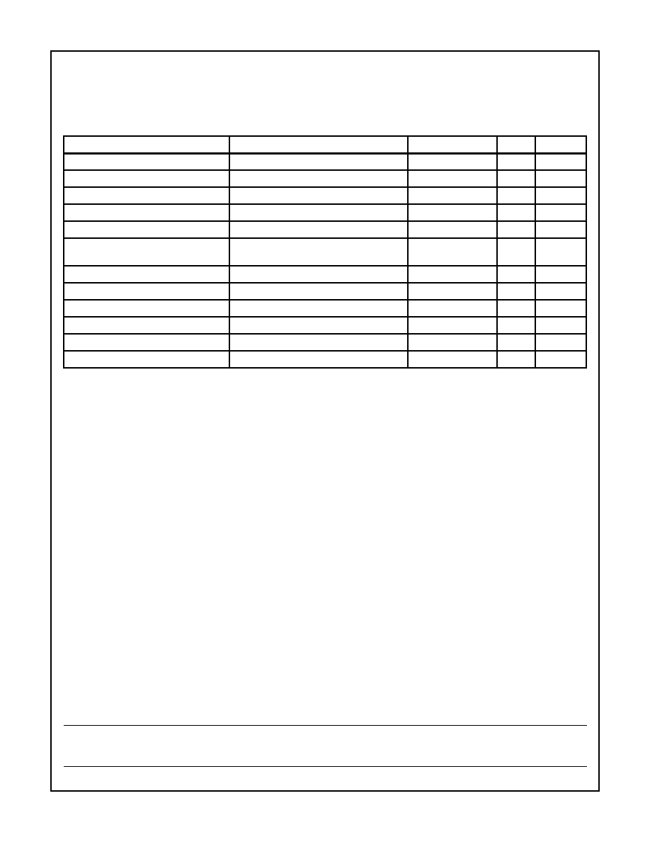
PARAMETER
CONDITIONS
TEMPERATURE
TYP
UNITS
Input Voltage Range
Full
±
10
V
Offset Voltage Drift
Full
30
µ
V/C
Gain Bandwidth Product (ChExt = 0pF)
Av = +1, V
O
= 200mVpp, R
L
= 2K, C
L
= 60pF
+25
o
C
10
MHz
Gain Bandwidth Product (ChExt = 100pF)
Av = +1, V
O
= 200mVpp, R
L
= 2K, C
L
= 60pF
+25
o
C
9.6
MHz
Gain Bandwidth Product (ChExt = 1000pF)
Av = +1, V
O
= 200mVpp, R
L
= 2K, C
L
= 60pF
+25
o
C
6.7
MHz
Full Power Bandwidth
V
O
= 20Vpp, R
L
= 2K, C
L
= 60pF, Slew Rate
Limited
+25
o
C
900
KHz
Output Resistance (Hold Mode)
+25
o
C
0.05
0.1% Acquisition Time
V
O
= 10V Step, R
L
= 2K, C
L
= 60pF
+25
o
C
430
ns
0.01% Acquisition Time
V
O
= 10V Step, R
L
= 2K, C
L
= 60pF
+25
o
C
700
ns
Effective Aperture Delay Time
+25
o
C
-15
ns
Aperture Uncertainty
+25
o
C
0.2
ns
1mV Hold Mode Settling Time
+25
o
C
200
ns
Spec Number
511117-883
All Intersil semiconductor products are manufactured, assembled and tested under ISO9000 quality systems certification.
Intersil products are sold by description only. Intersil Corporation reserves the right to make changes in circuit design and/or specifications at any time without
notice. Accordingly, the reader is cautioned to verify that data sheets are current before placing orders. Information furnished by Intersil is believed to be accurate
and reliable. However, no responsibility is assumed by Intersil or its subsidiaries for its use; nor for any infringements of patents or other rights of third parties which
may result from its use. No license is granted by implication or otherwise under any patent or patent rights of Intersil or its subsidiaries.
For information regarding Intersil Corporation and its products, see web site http://www.intersil.com