
1
HA-2640, HA-2645
4MHz, High Supply Voltage Operational
Amplifiers
HA-2640 and HA-2645 are monolithic operational amplifiers
which are designed to deliver unprecedented dynamic
specifications for a high voltage internally compensated
device. These dielectrically isolated devices offer very low
values for offset voltage and offset current coupled with large
output voltage swing and common mode input voltage.
For maximum reliability, these amplifiers offer unconditional
output overload protection through current limiting and a chip
temperature sensing circuit. This sensing device turns the
amplifier "off", when the chip reaches a certain temperature
level.
These amplifiers deliver
±
35V common mode input voltage
range,
±
35V output voltage swing, and up to
±
40V supply
range for use in such designs as regulators, power supplies,
and industrial control systems. 4MHz gain bandwidth and
5V/
µ
s slew rate make these devices excellent components
for high performance signal conditioning applications.
Outstanding input and output voltage swings coupled with a
low 5nA offset current make these amplifiers excitation
designs.
Features
∑ Output Voltage Swing . . . . . . . . . . . . . . . . . . . . . . . .
±
35V
∑ Supply Voltage . . . . . . . . . . . . . . . . . . . . . .
±
10V to
±
40V
∑ Offset Current. . . . . . . . . . . . . . . . . . . . . . . . . . . . . . . 5nA
∑ Bandwidth. . . . . . . . . . . . . . . . . . . . . . . . . . . . . . . . . 4MHz
∑ Slew Rate . . . . . . . . . . . . . . . . . . . . . . . . . . . . . . . . . 5V/
µ
s
∑ Common Mode Input Voltage Range . . . . . . . . . . . .
±
35V
∑ Output Overload Protection
Applications
∑ Industrial Control Systems
∑ Power Supplies
∑ High Voltage Regulators
∑ Resolver Excitation
∑ Signal Conditioning
Pinouts
Ordering Information
PART NUMBER
TEMP.
RANGE (
o
C)
PACKAGE
PKG.
NO.
HA2-2640-2
-55 to 125
8 Pin Metal Can
T8.C
HA2-2645-5
0 to 75
8 Pin Metal Can
T8.C
HA7-2640-2
-55 to 125
8 Ld CERDIP
F8.3A
HA7-2645-5
0 to 75
8 Ld CERDIP
F8.3A
HA-2640/2645
(CERDIP)
TOP VIEW
HA-2640/2645
(METAL CAN)
TOP VIEW
BAL
-IN
+IN
V-
1
2
3
4
8
7
6
5
COMP
V+
OUT
BAL
-
+
COMP
OUT
-IN
V-
BAL
+IN
V+
BAL
2
4
6
1
3
7
5
8
-
+
(TO-99 CASE VOLTAGE = FLOATING)
Data Sheet
September 1998
File Number
2904.3
CAUTION: These devices are sensitive to electrostatic discharge; follow proper IC Handling Procedures.
1-888-INTERSIL or 321-724-7143
|
Copyright
©
Intersil Corporation 1999
2
Absolute Maximum Ratings
Thermal Information
Voltage Between V+ and V- Terminals. . . . . . . . . . . . . . . . . . . 100V
Differential Input Voltage Range . . . . . . . . . . . . . . . . . . . . . . . . 37V
Output Current . . . . . . . . . . . . . . . . . . . . Full Short Circuit Protection
Operating Conditions
Temperature Range
HA-2640-2 . . . . . . . . . . . . . . . . . . . . . . . . . . . . . . -55
o
C to 125
o
C
HA-2645-5 . . . . . . . . . . . . . . . . . . . . . . . . . . . . . . . . 0
o
C to 75
o
C
Thermal Resistance (Typical, Note 1)
JA
(
o
C/W)
JC
(
o
C/W)
CERDIP Package . . . . . . . . . . . . . . . . .
135
50
Metal Can Package . . . . . . . . . . . . . . .
165
80
Maximum Junction Temperature . . . . . . . . . . . . . . . . . . . . . . . .175
o
C
Maximum Storage Temperature Range . . . . . . . . . . -65
o
C to 150
o
C
Maximum Lead Temperature (Soldering 10s) . . . . . . . . . . . . 300
o
C
CAUTION: Stresses above those listed in "Absolute Maximum Ratings" may cause permanent damage to the device. This is a stress only rating and operation of the
device at these or any other conditions above those indicated in the operational sections of this specification is not implied.
NOTE:
1.
JA
is measured with the component mounted on an evaluation PC board in free air.
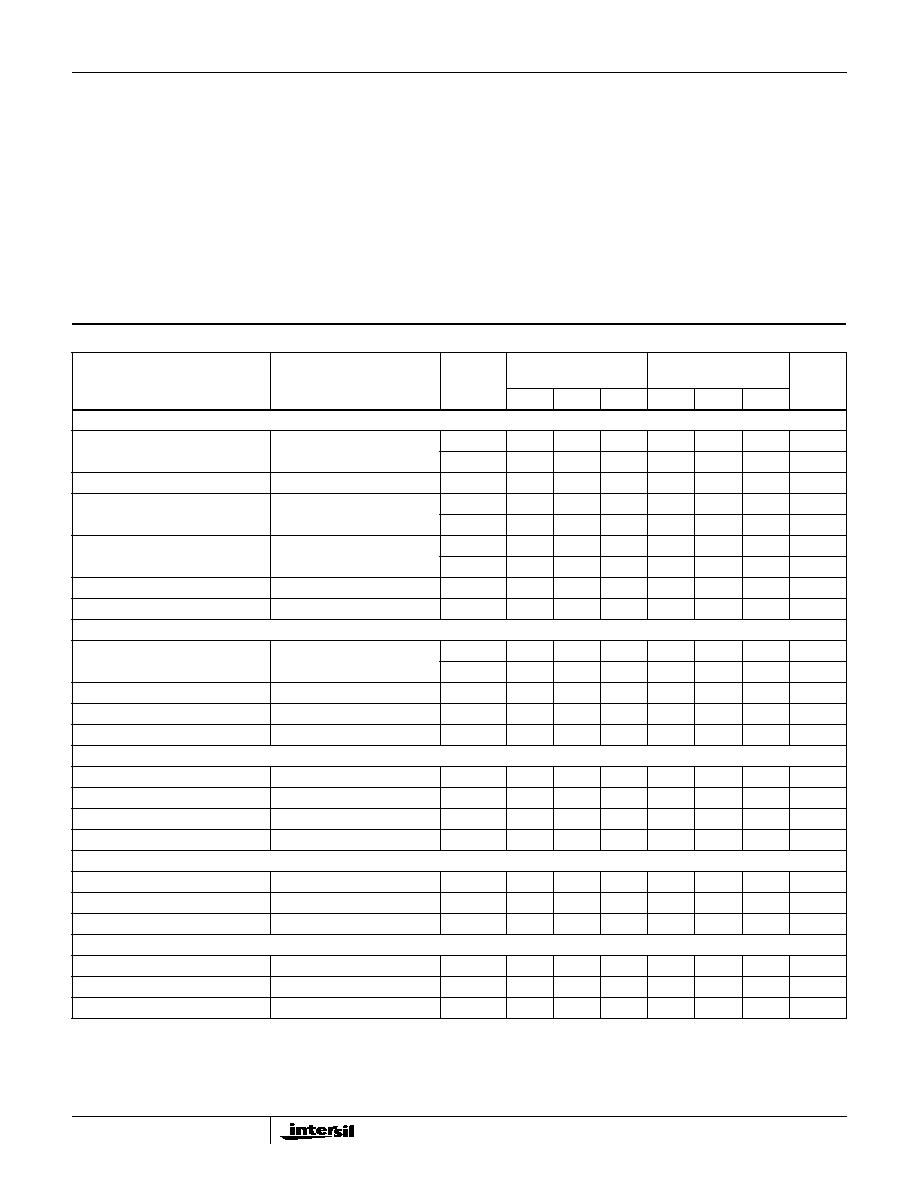
Electrical Specifications
V
SUPPLY
=
±
40V, R
L
= 5k
, Unless Otherwise Specified
PARAMETER
TEST CONDITIONS
TEMP
(
o
C)
HA-2640-2
-55
o
C TO 125
o
C
HA-2645-5
0
o
C TO 75
o
C
UNITS
MIN
TYP
MAX
MIN
TYP
MAX
INPUT CHARACTERISTICS
Offset Voltage
25
-
2
4
-
2
6
mV
Full
-
6
-
-
7
mV
Average Offset Voltage Drift
Full
-
15
-
-
15
-
µ
V/
o
C
Bias Current
25
-
10
25
-
12
30
nA
Full
-
-
50
-
-
50
nA
Offset Current
25
-
5
12
-
15
30
nA
Full
-
-
35
-
-
50
nA
Input Resistance (Note 2)
25
50
250
-
40
200
-
M
Common Mode Range
Full
±
35
-
-
±
35
-
-
V
TRANSFER CHARACTERISTICS
Large Signal Voltage Gain
V
OUT
=
±
30V
25
100
200
-
100
200
-
kV/V
Full
75
-
-
75
-
-
kV/V
Common Mode Rejection Ratio
V
CM
=
±
20V
Full
80
100
-
74
100
-
dB
Minimum Stable Gain
25
1
-
-
1
-
-
V/V
Unity Gain Bandwidth
V
OUT
= 90mV
25
-
4
-
-
4
-
MHz
OUTPUT CHARACTERISTICS
Output Voltage Swing
Full
±
35
-
-
±
35
-
-
V
Output Current
R
L
= 1k
25
±
12
±
15
-
±
10
±
12
-
mA
Output Resistance
Open Loop
25
-
500
-
-
500
-
Full Power Bandwidth (Note 3)
V
OUT
=
±
35V
25
-
23
-
-
23
-
kHz
TRANSIENT RESPONSE A
V
= +1, C
L
= 50pF, R
L
= 5k
Rise Time
V
OUT
=
±
200mV
25
-
60
135
-
60
135
ns
Overshoot
V
OUT
=
±
200mV
25
-
15
30
15
40
%
Slew Rate
25
±
3
±
5
-
±
2.5
±
5
-
V/
µ
s
POWER SUPPLY CHARACTERISTICS
Supply Current
25
-
3.2
3.8
-
3.2
4.5
mA
Supply Voltage Range
Full
±
10
-
±
40
±
10
-
±
40
V
Power Supply Rejection Ratio
V
S
=
±
10V to
±
40V
Full
80
90
-
74
90
-
dB
NOTES:
2. This parameter is based upon design calculations.
3. Full Power Bandwidth guaranteed based upon slew rate measurement: FPBW = S.R./2
V
PEAK
; V
PEAK
= 35V.
HA-2640, HA-2645

3
Schematic Diagram
Test Circuits and Waveform
FIGURE 1. SLEW RATE AND TRANSIENT RESPONSE TEST
CIRCUIT
NOTE: Tested offset adjustment range is |V
OS
+1mV| minimum
referred to output. Typical range is
±
20mV with R
T
= 10k
.
FIGURE 2. SUGGESTED V
OS
ADJUSTMENT AND
COMPENSATION HOOK UP
BAL
BAL
5
1
2 -IN
6
V
OUT
D
11
D
16
D
15
R
23
R
24
Q
59
Q
57
Q
60
Q
58
Q
55
R
22
R
21
Q
53
Q
51
Q
56
Q
54
Q
52
Q
50
Q
49
R
20
R
19
R
18
R
17
R
27
R
26
Q
44
Q
41
R
16
R
15
R
14
R
13
Q
48
C
2
Q
42
C
3
C
4
C
1
Q
43
D
12
Q
47
Q
46
14
D
10
R
11
R
10
Q
11
R
3
R
2
Q9
Q
10
Q
8
Q
13
Q
6
Q
4
D
2
D
3
Q
12
Q
19
D
4
D
5
D
6
D
7
Q
7
Q
5
Q
3
R
4
Q
61
Q
1
R
1
R
25
D
17
R
25
R
5
R
6
R
7
R
8
R
9
R
12
Q
15
Q
17
Q
34
Q
28
Q
30
Q
18
Q
35
Q
31
Q
29
Q
40
Q
36
Q
37
Q
38
Q
39
Q
32
Q
33
Q
24
Q
23
Q
22
Q
21
Q
20
Q
25
Q
26
Q
27
D
13
7
V+
4
V-
Q
16
3 +IN
D
8
D
9
8 COMP
50pF
OUT
IN
5K
+
V-
V+
-
2
4
6
1
3
7
5
8
-
+
COMP
CAP
V-
10k
HA-2640, HA-2645

4
NOTE: R
L
= 5k
, C
L
= 50pF, T
A
= 25
o
C, V
S
=
±
40V
FIGURE 3. VOLTAGE FOLLOWER PULSE RESPONSE
Test Circuits and Waveform
(Continued)
Vertical = 10V/Div., Horizontal = 5
µ
s/Div.
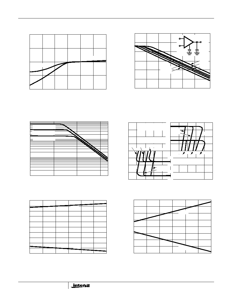
Typical Performance Curves
V
S
=
±
40V, T
A
= 25
o
C, Unless Otherwise Specified
FIGURE 4. INPUT BIAS AND OFFSET CURRENT vs
TEMPERATURE
FIGURE 5. INPUT NOISE CHARACTERISTICS
FIGURE 6. NORMALIZED AC PARAMETERS vs TEMPERATURE
FIGURE 7. OPEN LOOP FREQUENCY RESPONSE
TEMPERATURE (
o
C)
0
-50
-25
25
50
75
100
125
CURRENT (nA)
25
20
15
10
5
0
BIAS CURRENT
OFFSET CURRENT
FREQUENCY (Hz)
100K
10K
1K
100
10
1
INPUT NOISE V
O
L
T
A
GE (nV/
Hz)
1
10
100
1000
INPUT NOISE CURRENT
INPUT NOISE VOLTAGE
0.01
0.1
1
10
INPUT NOISE CURRENT (pA/
Hz)
TEMPERATURE (
o
C)
0
-50
-25
25
50
75
100
125
1.4
1.2
1.0
0.8
SLEW RATE
BANDWIDTH
NORMALIZED V
ALUE REFERRED T
O
25
o
C
FREQUENCY (Hz)
100K
10K
1K
100
10
1M
10M
270
225
180
135
90
45
0
-40
0
40
80
120
PHASE
GAIN
OPEN LOOP V
O
L
T
A
GE GAIN (dB)
PHASE ANGLE (DEGREES)
HA-2640, HA-2645
5
FIGURE 8. NORMALIZED AC PARAMETERS vs SUPPLY
VOLTAGE AT 25
o
C
FIGURE 9. OPEN LOOP FREQUENCY RESPONSE FOR
VARIOUS VALUES OF CAPACITORS FROM
COMPENSATION PIN TO GROUND
FIGURE 10. OUTPUT VOLTAGE SWING vs FREQUENCY
FIGURE 11. OUTPUT CURRENT CHARACTERISTIC
FIGURE 12. SUPPLY CURRENT vs SUPPLY VOLTAGE
FIGURE 13. OUTPUT VOLTAGE SWING vs SUPPLY VOLTAGE
Typical Performance Curves
V
S
=
±
40V, T
A
= 25
o
C, Unless Otherwise Specified (Continued)
SUPPLY VOLTAGE (
±
V)
0.8
SLEW RATE
BANDWIDTH
10
20
30
40
0.9
1.0
1.1
1.2
NORMALIZED V
ALUE REFERRED T
O
±
30V
FREQUENCY (Hz)
100K
10K
1K
100
10
1M
10M
0pF
30pF
100pF
300pF
1,000pF
OPEN LOOP GAIN (dB)
40
0
40
80
120
AUT
C
COMP
C
L
=
100pF
V
SUPPLY
=
±
40V
V
SUPPLY
=
±
20V
V
SUPPLY
=
±
10V
FREQUENCY (Hz)
1K
100K
1M
10K
0.1
1.0
10.0
100
OUTPUT V
O
L
T
A
GE SWING (V
P-P
)
OUTPUT LOAD CURRENT (mA)
-10
-20
-40
-30
A
V
= 1, V
SUPPLY
=
±
40V
V
IN
= -35V
A
V
= 1, V
SUPPLY
=
±
20V
V
IN
= -15V
125
o
C
25
o
C
-55
o
C
OUTPUT V
O
L
T
A
GE (V)
20
15
10
5
125
o
C
-55
o
C
25
o
C
10
20
40
30
A
V
= 1, V
SUPPLY
=
±
40V
V
IN
= +35V
A
V
= 1, V
SUPPLY
=
±
20V
V
IN
= +15V
125
o
C
25
o
C
-10
-5
-55
o
C
-15
-20
-55
o
C
125
o
C
25
o
C
SUPPLY VOLTAGE (
±
V)
SUPPL
Y CURRENT (mA)
10
15
20
25
30
35
40
-2.5
-2.0
-1.5
-1.0
-0.5
0
0.5
1.0
1.5
2.0
2.5
+I
CC
-I
CC
SUPPLY VOLTAGE (
±
V)
OUTPUT V
O
L
T
A
GE SWING (
±
V)
10
15
20
25
30
35
40
-40
-V
OUT
+V
OUT
-30
-20
-10
0
10
20
30
40
HA-2640, HA-2645

6
All Intersil semiconductor products are manufactured, assembled and tested under ISO9000 quality systems certification.
Intersil semiconductor products are sold by description only. Intersil Corporation reserves the right to make changes in circuit design and/or specifications at any time with-
out notice. Accordingly, the reader is cautioned to verify that data sheets are current before placing orders. Information furnished by Intersil is believed to be accurate and
reliable. However, no responsibility is assumed by Intersil or its subsidiaries for its use; nor for any infringements of patents or other rights of third parties which may result
from its use. No license is granted by implication or otherwise under any patent or patent rights of Intersil or its subsidiaries.
For information regarding Intersil Corporation and its products, see web site www.intersil.com
Sales Office Headquarters
NORTH AMERICA
Intersil Corporation
P. O. Box 883, Mail Stop 53-204
Melbourne, FL 32902
TEL: (321) 724-7000
FAX: (321) 724-7240
EUROPE
Intersil SA
Mercure Center
100, Rue de la Fusee
1130 Brussels, Belgium
TEL: (32) 2.724.2111
FAX: (32) 2.724.22.05
ASIA
Intersil (Taiwan) Ltd.
7F-6, No. 101 Fu Hsing North Road
Taipei, Taiwan
Republic of China
TEL: (886) 2 2716 9310
FAX: (886) 2 2715 3029
Die Characteristics
DIE DIMENSIONS:
93 mils x 68 mils x 19 mils
2360
µ
m x 1720
µ
m x 483
µ
m
METALLIZATION:
Type: Al, 1% Cu
Thickness: 16k
≈
±
2k
≈
PASSIVATION:
Type: Nitride (Si
3
N
4
) over Silox (SiO
2
, 5% Phos.)
Silox Thickness: 12k
≈
±
2k
≈
Nitride Thickness: 3.5k
≈
±
1.5k
≈
SUBSTRATE POTENTIAL (Powered Up):
Unbiased
TRANSISTOR COUNT:
76
PROCESS:
HV200 Bipolar Dielectric Isolation
Metallization Mask Layout
HA-2640, HA-2645
COMP
V+
OUT
BAL
V-
+IN
-IN
BAL
HA-2640, HA-2645