 | –≠–ª–µ–∫—Ç—Ä–æ–Ω–Ω—ã–π –∫–æ–º–ø–æ–Ω–µ–Ω—Ç: HA-2405 | –°–∫–∞—á–∞—Ç—å:  PDF PDF  ZIP ZIP |

1
Æ
HA-2404
40MHz, PRAM Four Channel
Programmable Amplifiers
The HA-2404 comprise a series of four-channel
programmable amplifiers providing a level of versatility
unsurpassed by any other monolithic operational amplifier.
Versatility is achieved by employing four input amplifier
channels, any one (or none) of which may be electronically
selected and connected to a single output stage through
DTL/TTL compatible address inputs. The device formed by
the output and the selected pair of inputs is an op amp which
delivers excellent slew rate, gain bandwidth and power
bandwidth performance. Other advantageous features for
these dielectrically isolated amplifiers include high voltage
gain and input impedance coupled with low input offset
voltage and offset current. External compensation is not
required on this device at closed loop gains greater than 10.
Each channel of the HA-2404 can be controlled and
operated with suitable feedback networks in any of the
standard op amp configurations. This specialization makes
these amplifiers excellent components for multiplexing signal
selection and mathematical function designs. With 30V/
µ
s
slew rate, 40MHz gain bandwidth and 30M
input
impedance these devices are ideal building blocks for signal
generators, active filters and data acquisition designs.
Programmability, coupled with 4mV typical offset voltage
and 5nA offset current, makes these amplifiers outstanding
components for signal conditioning circuits.
During Disable Mode V
OUT
goes to V-. For high output
impedance during Disable, see HA2444.
For further design ideas, see Application Note AN514.
Features
∑ Programmability
∑ High Rate Slew . . . . . . . . . . . . . . . . . . . . . . . . . . . 30V/
µ
s
∑ Wide Gain Bandwidth. . . . . . . . . . . . . . . . . . . . . . . 40MHz
∑ High Gain . . . . . . . . . . . . . . . . . . . . . . . . . . . . . . . 150kV/V
∑ Low Offset Current . . . . . . . . . . . . . . . . . . . . . . . . . . . .5nA
∑ High Input Impedance . . . . . . . . . . . . . . . . . . . . . . . 30M
∑ Single Capacitor Compensation
∑ DTL/TTL Compatible Inputs
Applications
∑ Thousands of Applications; Program
- Signal Selection/Multiplexing
- Operational Amplifier Gain
- Oscillator Frequency
- Filter Characteristics
- Add-Subtract Functions
- Integrator Characteristics
- Comparator Levels
Pinout
HA-2404 (CERDIP)
TOP VIEW
Ordering Information
PART NUMBER
TEMP.
RANGE (
o
C)
PACKAGE
PKG.
DWG. #
HA1-2404-4
-25 to 85
16 Ld CERDIP
F16.3
TRUTH TABLE
D1
D0
EN
SELECTED CHANNEL
D1
L
L
H
1
L
L
H
H
2
L
H
L
H
3
H
H
H
H
4
H
X
X
L
None, V
OUT
goes to V-
X
14
15
16
9
13
12
11
10
1
2
3
4
5
7
6
8
3
OUTPUT AMP
ENABLE
D0
D1
GND
COMP
V+
OUT
V-
4
1
2
+IN3
-IN3
+IN4
-IN4
-IN1
+IN1
+IN2
-IN2
3
DECODE
CONTROL
+
-
+
-
+
-
+
-
August 2003
Data Sheet
FN2891.5
CAUTION: These devices are sensitive to electrostatic discharge; follow proper IC Handling Procedures.
1-888-INTERSIL or 321-724-7143
|
Intersil (and design) is a registered trademark of Intersil Americas Inc.
Copyright © Intersil Americas Inc. 2003. All Rights Reserved
All other trademarks mentioned are the property of their respective owners.
2
Absolute Maximum Ratings
(T
A
= 25∞C)
Thermal Information
Voltage Between V+ and V- Terminals . . . . . . . . . . . . . . . . . 45.0V
Differential Input Voltage . . . . . . . . . . . . . . . . . . . . . . . . . . V
SUPPLY
Digital Input Voltage . . . . . . . . . . . . . . . . . . . . . . . . -0.76V to +10.0V
Output Current . . . . . . . . . . . Short Circuit Protected, I
SC
<
±
33mA)
Internal Power Dissipation (Note 1)
Operating Conditions
Temperature Range
HA-2404-4 . . . . . . . . . . . . . . . . . . . . . . . . . . . . . . . -25
o
C to 85
o
C
Thermal Resistance (Typical, Note 2)
JA
(
o
C/W)
JC
(
o
C/W)
CERDIP Package . . . . . . . . . . . . . .
75
22
Maximum Junction Temperature (Ceramic Package) . . . . . . . . 175
o
C
Maximum Junction Temperature (Plastic Package) . . . . . . . 150
o
C
Maximum Storage Temperature Range . . . . . . . . . -65
o
C to 150
o
C
Maximum Lead Temperature (Soldering 10s) . . . . . . . . . . . . 300
o
C
CAUTION: Stresses above those listed in "Absolute Maximum Ratings" may cause permanent damage to the device. This is a stress only rating and operation of the
device at these or any other conditions above those indicated in the operational sections of this specification is not implied.
NOTES:
1. Maximum power dissipation including output load, must be designed to maintain the junction temperature below 175
o
C for the ceramic package,
and below 150
o
C for the plastic packages.
2.
JA is measured with the component mounted on a low effective thermal conductivity test board in free air. See Tech Brief TB379 for details.
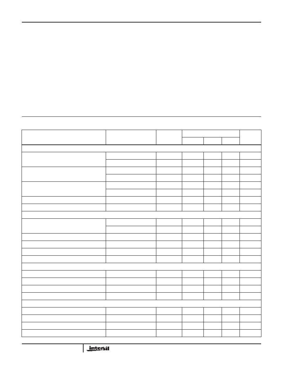
Electrical Specifications
Test Conditions: V
SUPPLY
=
±
15V, Unless Otherwise Specified. Digital Inputs: V
IL
= +0.5V, V
IH
= +2.4. Limits
apply to each of the four channels, when addressed
PARAMETER
TEST
CONDITIONS
TEMP.
(
o
C)
HA-2404
UNITS
MIN
TYP
MAX
INPUT CHARACTERISTICS
Offset Voltage
25
-
4
9
mV
Full
-
-
11
mV
Bias Current (Note 8)
25
-
50
200
nA
Full
-
-
400
nA
Offset Current (Note 8)
25
-
5
50
nA
Full
-
-
100
nA
Input Resistance (Note 8)
25
-
30
-
M
Common Mode Range
Full
±
9.0
-
-
V
TRANSFER CHARACTERISTICS
Large Signal Voltage Gain
R
L
= 2k
25
50
150
-
kV/V
V
OUT
= 20V
P-P
Full
25
-
-
kV/V
Common Mode Rejection Ratio
V
CM
=
±
5V
Full
80
100
-
dB
Gain Bandwidth (Notes 3, 9)
25
20
40
-
MHz
Gain Bandwidth (Notes 4, 9)
25
4
8
-
MHz
Minimum Stable Gain
(C
COMP
= 0)
10
-
-
V/V
OUTPUT CHARACTERISTICS
Output Voltage Swing
R
L
= 2k
Full
±
10.0
±
12.0
-
V
Output Current
25
10
20
-
mA
Full Power Bandwidth (Notes 3, 10)
V
OUT
= 20V
P-P
25
640
950
-
kHz
Full Power Bandwidth (Notes 4, 10)
V
OUT
= 20V
P-P
25
200
250
-
kHz
TRANSIENT RESPONSE (Note 11)
Rise Time (Note 4)
V
OUT
= 200mV
PEAK
25
-
20
45
ns
Overshoot (Note 4)
V
OUT
= 200mV
PEAK
25
-
25
40
%
Slew Rate (Note 3)
V
OUT
= 10V
P-P
25
20
30
-
V/
µ
s
Slew Rate (Notes 4, 9)
V
OUT
= 10V
P-P
25
6
8
-
V/
µ
s
HA-2404

3
Settling Time (Notes 4, 5, 9)
V
OUT
= 10V
P-P
25
-
1.5
2.5
µ
s
CHANNEL SELECT CHARACTERISTICS
Digital Input Current
V
IN
= 0V
Full
-
1
1.5
mA
Digital Input Current
V
IN
= +5.0V
Full
-
5
-
nA
Output Delay (Notes 6, 9)
25
-
100
250
ns
Crosstalk (Note 7)
25
-80
-110
-
dB
POWER SUPPLY CHARACTERISTICS
Supply Current
25
-
4.8
6.0
mA
Power Supply Rejection Ratio
V
S
=
±
10V to
±
20V
Full
74
90
-
dB
NOTES:
3. A
V
= +10, C
COMP
= 0, R
L
= 2k
, C
L
= 50pF.
4. A
V
= +1, C
COMP
= 15pF, R
L
= 2k
, C
L
= 50pF.
5. To 0.1% of final value.
6. To 10% of final value; output then slews at normal rate to final value.
7. Unselected input to output; V
IN
=
±
10V
DC
.
8. Unselected channels have approximately the same input parameters.
9. Guaranteed by design.
10. Full Power Bandwidth based on slew rate measurement using:
.
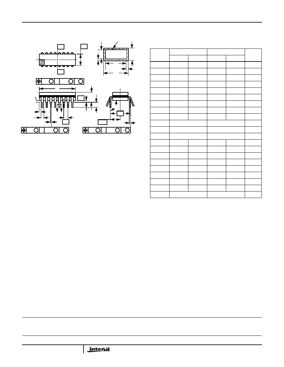
11. See Figure 13 for test circuit.
Electrical Specifications
Test Conditions: V
SUPPLY
=
±
15V, Unless Otherwise Specified. Digital Inputs: V
IL
= +0.5V, V
IH
= +2.4. Limits
apply to each of the four channels, when addressed (Continued)
PARAMETER
TEST
CONDITIONS
TEMP.
(
o
C)
HA-2404
UNITS
MIN
TYP
MAX
FPBW
SR
2
VPEAK
--------------------------- VPEAK
;
5V
=
=
HA-2404
HA-2404

4
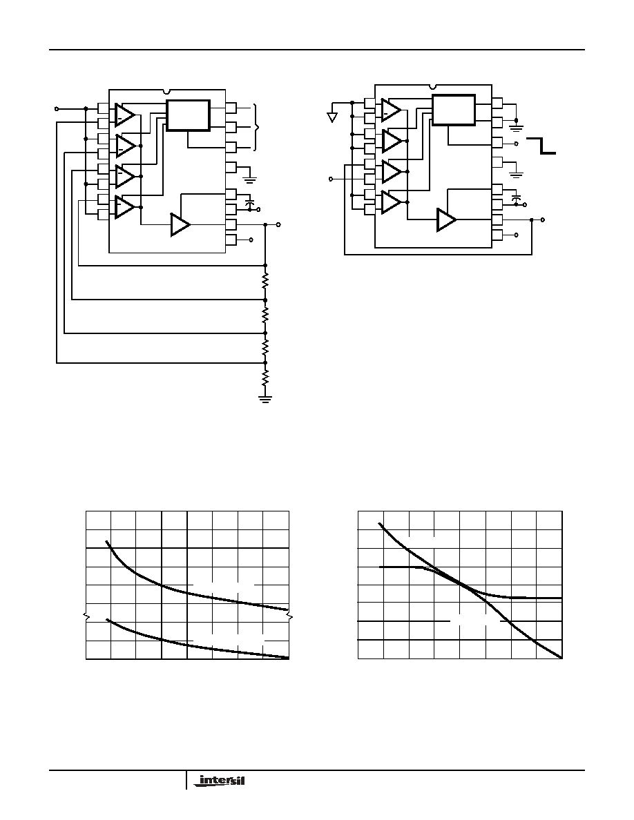
Schematic Diagram
HA-2404
ENABLE
GND
OUT
R
2
2.4K
R
4
22.9K
Q
1
Q
3
Q
4
Q
6
Q
7
Q
8
R
1
1.6K
R
3
1.8K
Q
2
Q
5
R
5
8.0K
R
6
2.0K
R
35
1.6K
R
7
5.6K
Q
10
Q
11
Q
13
Q
12
Q
15
Q
14
R
8
4K
Q
16
R
9
1.5K
R
10
10K
R
11
10K
VA
VC
Q17
VB
Q
18
Q
19
Q
20
VD
R
12
1.6K
Q
28
VE
R
13
0.8K
Q
22
R
15
10K
R
16
10K
Q
21
Q
26
Q
27
R
14
10K
Q
29
Q
23
Q
24
Q
25
Q
30
Q
32
Q
33
Q
102
Q
34
Q
38
R
18
2.0K
Q
103
Q
35
Q
31
Q
36
Q
37
Q
39
Q
40
Q
41
Q
79
Q
81
Q
82
Q
84
Q
80
Q
83
Q
86
Q
89
Q
88
R
35
0.75K
Q
85
Q
98
Q
92
R
30
1.2K
C
1
9.0pF
V+
Q
93
Q
42
R19
1.6K
TO ADDITIONAL
INPUT STAGES
R
29
0.4K
Q
90
Q
91
R
33
4K
Q
97
Q
100
Q
99
Q
95
Q
94
+V
CC
-V
EE
R
31
36.5
R
32
34
Q
96
COMP
IN-
IN+
D1
D0
R
17
1.6K
Q
87
R
34
1.6K
Q
101
Q
9
Diagram Includes: One Input Stage, Decode Control, Bias Network, and Output Stage
HA-2404
HA-2404
5
Typical Applications
FIGURE 1. HA-2404 AMPLIFIER, NONINVERTING
PROGRAMMABLE GAIN
FIGURE 2. HA-2404 SAMPLE AND HOLD
For more examples, see Intersil Application Note AN514.
+ 2
1K
500
500
ENABLE
GND
COMP
OUTPUT
AMP
V-
13
8
1
2
3
4
5
7
6
V+
+
4
+
3
+
1
14
15
16
12
11
10
9
+
D1
D0
15pF
IN
2K
-15V
DECODE/
CONTROL
DIGITAL
DIGITAL
GROUND
CONTROL
+15V
OUT
1
ENABLE
GND
COMP
OUTPUT
AMP
V-
13
8
1
2
3
4
5
7
6
V+
+
4
+
3
+
+2
14
15
16
12
11
10
9
D1
D0
-15V
DIGITAL
GROUND
+15V
C
OUT
S
H
IN
DECODE/
CONTROL
I
1
150 x 10
-6
A
I
2
200 x 10
-9
A at 25
o
C
600 x 10
-9
A at -55
o
C
100 x 10
-9
A at 125
o
C
Q
2 x 10
-12
C
Sample Charging Rate
I1
C
-----V
s
/
=
Hold Drift Rate
I2
C
-----V
s
/
=
Switch Pedestal Error
Q
C
----V
=
-
-
-
Typical Performance Curves
FIGURE 3. INPUT BIAS CURRENT AND OFFSET CURRENT vs
TEMPERATURE
FIGURE 4. NORMALIZED AC PARAMETERS vs TEMPERATURE
TEMPERATURE (
o
C)
-55
-50
-25
0
25
50
75
100
125
CURRENT (nA)
0
5
10
40
60
80
100
120
140
BIAS CURRENT
OFFSET CURRENT
TEMPERATURE (
o
C)
-55
-50
-25
0
25
50
75
100
125
N
O
RMAL
IZED VALUE R
E
FERRED T
O
2
5
o
C
0.8
0.9
1.0
1.1
1.2
BANDWIDTH
SLEW RATE
HA-2404
HA-2404

6
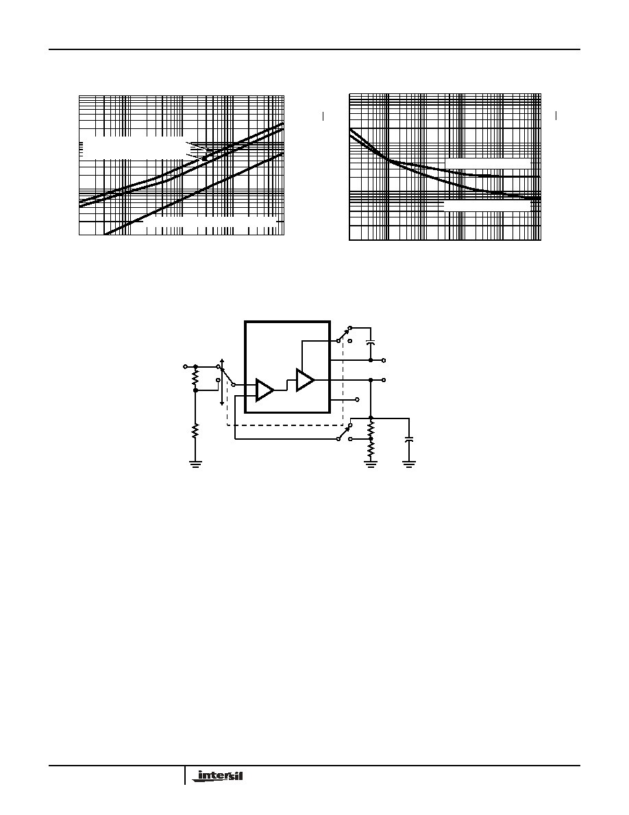
FIGURE 5. POWER SUPPLY CURRENT vs TEMPERATURE
FIGURE 6. OPEN LOOP FREQUENCY AND PHASE RESPONSE
FIGURE 7. FREQUENCY RESPONSE vs C
COMP
FIGURE 8. NORMALIZED AC PARAMETERS vs SUPPLY
VOLTAGE
FIGURE 9. OPEN LOOP VOLTAGE GAIN vs TEMPERATURE
FIGURE 10. OUTPUT VOLTAGE SWING vs FREQUENCY
Typical Performance Curves
(Continued)
TEMPERATURE (
o
C)
-55
-50
-25
0
25
50
75
100
125
S
U
P
P
LY CURR
E
N
T
(mA)
3
4
5
V
SUPPLY
=
±
20V
V
SUPPLY
=
±
15V
V
SUPPLY
=
±
10V
CROSSTALK REJECTION, A
V
= +1
C
COMP
= 0pF
PHASE
C
COMP
= 15pF
GAIN
OP
EN LO
OP
VO
LTAG
E GAI
N
(dB)
-20
0
20
40
60
80
100
120
FREQUENCY (Hz)
10
100
1K
10K
100K
1M
10M
100M
0
30
60
90
120
150
180
210
P
H
A
S
E (
D
EG
R
E
E
S
)
FREQUENCY (Hz)
10
100
1K
10K
100K
1M
10M
100M
OPEN LO
O
P
VO
LTAG
E
G
A
IN
(dB)
-20
0
20
40
60
80
100
120
1000pF
300pF
100pF
30pF
15pF
0pF
SLEW RATE
BANDWIDTH
SUPPLY VOLTAGE (V)
±
10
±
20
±
15
0.8
0.9
1.0
1.1
1.2
NORMALIZED
V
A
LUE RE
FERRE
D TO
±
15
V
TEMPERATURE (
o
C)
-55
-50
-25
0
25
50
75
100
125
GAI
N
(
d
B)
90
100
110
V
SUPPLY
=
±
20V
V
SUPPLY
=
±
15V
V
SUPPLY
=
±
10V
105
95
FREQUENCY (Hz)
10K
100K
1M
10M
O
U
TP
UT S
W
IN
G
(V
P-P
)
0.1
1.0
10
20
C
COMP
= 0pF
C
COMP
= 15pF
HA-2404
HA-2404
7
FIGURE 11. EQUIVALENT INPUT NOISE vs BANDWIDTH
FIGURE 12. INPUT NOISE vs FREQUENCY
FIGURE 13. SLEW RATE AND TRANSIENT RESPONSE
Typical Performance Curves
(Continued)
100Hz
1kHz
10kHz
100kHz
1MHz
UPPER 3dB FREQUENCY (LOWER 3dB FREQUENCY-10Hz)
BROADBAND NOISE CHARACTERISTICS
INP
U
T NOI
SE (
µ
V)
100
10
1.0
0.1
0 SOURCE RESISTANCE
10K SOURCE RESISTANCE
THERMAL NOISE OF 10K RESISTOR
1
100
1K
10K
100K
10
FREQUENCY (Hz)
INP
U
T NOISE CURRENT
(
p
A/
Hz
)
I
N
PUT NO
IS
E
VOLTAGE
(nV
/
Hz
)
1000
100
10
1
10
1
0.1
0.01
INPUT NOISE VOLTAGE
INPUT NOISE CURRENT
COMP
A
V
= 1
IN
15pF
+15.0V
OUT
SELECTED
CHANNEL
-15.0V
1800
200
+
-
A
V
= 10
50pF
45
5
HA-2404
8
All Intersil U.S. products are manufactured, assembled and tested utilizing ISO9000 quality systems.
Intersil Corporation's quality certifications can be viewed at www.intersil.com/design/quality
Intersil products are sold by description only. Intersil Corporation reserves the right to make changes in circuit design, software and/or specifications at any time without
notice. Accordingly, the reader is cautioned to verify that data sheets are current before placing orders. Information furnished by Intersil is believed to be accurate and
reliable. However, no responsibility is assumed by Intersil or its subsidiaries for its use; nor for any infringements of patents or other rights of third parties which may result
from its use. No license is granted by implication or otherwise under any patent or patent rights of Intersil or its subsidiaries.
For information regarding Intersil Corporation and its products, see www.intersil.com
HA-2404
Ceramic Dual-In-Line Frit Seal Packages (CERDIP)
NOTES:
1. Index area: A notch or a pin one identification mark shall be locat-
ed adjacent to pin one and shall be located within the shaded
area shown. The manufacturer's identification shall not be used
as a pin one identification mark.
2. The maximum limits of lead dimensions b and c or M shall be
measured at the centroid of the finished lead surfaces, when
solder dip or tin plate lead finish is applied.
3. Dimensions b1 and c1 apply to lead base metal only. Dimension
M applies to lead plating and finish thickness.
4. Corner leads (1, N, N/2, and N/2+1) may be configured with a
partial lead paddle. For this configuration dimension b3 replaces
dimension b2.
5. This dimension allows for off-center lid, meniscus, and glass
overrun.
6. Dimension Q shall be measured from the seating plane to the
base plane.
7. Measure dimension S1 at all four corners.
8. N is the maximum number of terminal positions.
9. Dimensioning and tolerancing per ANSI Y14.5M - 1982.
10. Controlling dimension: INCH.
bbb
C A - B
S
c
Q
L
A
SEATING
BASE
D
PLANE
PLANE
-D-
-A-
-C-
-B-
D
E
S1
b2
b
A
e
M
c1
b1
(c)
(b)
SECTION A-A
BASE
LEAD FINISH
METAL
e
A/2
A
M
S
S
ccc
C A - B
M
D
S
S
aaa
C A - B
M
D
S
S
e
A
F16.3
MIL-STD-1835 GDIP1-T16 (D-2, CONFIGURATION A)
16 LEAD CERAMIC DUAL-IN-LINE FRIT SEAL PACKAGE
SYMBOL
INCHES
MILLIMETERS
NOTES
MIN
MAX
MIN
MAX
A
-
0.200
-
5.08
-
b
0.014
0.026
0.36
0.66
2
b1
0.014
0.023
0.36
0.58
3
b2
0.045
0.065
1.14
1.65
-
b3
0.023
0.045
0.58
1.14
4
c
0.008
0.018
0.20
0.46
2
c1
0.008
0.015
0.20
0.38
3
D
-
0.840
-
21.34
5
E
0.220
0.310
5.59
7.87
5
e
0.100 BSC
2.54 BSC
-
eA
0.300 BSC
7.62 BSC
-
eA/2
0.150 BSC
3.81 BSC
-
L
0.125
0.200
3.18
5.08
-
Q
0.015
0.060
0.38
1.52
6
S1
0.005
-
0.13
-
7
90
o
105
o
90
o
105
o
-
aaa
-
0.015
-
0.38
-
bbb
-
0.030
-
0.76
-
ccc
-
0.010
-
0.25
-
M
-
0.0015
-
0.038
2, 3
N
16
16
8
Rev. 0 4/94