3-1
CAUTION: These devices are sensitive to electrostatic discharge; follow proper IC Handling Procedures.
1-888-INTERSIL or 321-724-7143
|
Copyright
©
Intersil Corporation 1999
HA-2444/883
Selectable, Four Channel
Video Operational Amplifier
Description
The HA-2444/883 is a channel-selectable video op amp consisting
of four differential inputs, a single-ended output, and digital control
circuitry allowing two digital inputs to activate one of the four differ-
ential inputs. The HA-2444/883 also includes a high impedance
output state allowing the outputs of multiple HA-2444/883s to be
wire-OR'd. Functionally, the HA-2444/883 is equivalent to four
wideband video op amps and a wideband multiplexer.
Unlike similar competitor devices, the HA-2444/883 is not
restricted to multiplexing. Any op amp configuration can be used
with any of the inputs. Signal amplification, addition, integration,
and more can be put under digital control with broadcast quality
performance.
The key video parameters of the HA-2444/883 have been opti-
mized without compromising DC performance. Gain Flatness, to
10MHz, is only 0.12dB. Differential gain and phase are typically
0.03% and 0.03 degrees, respectively.
Laser trimming allows offset voltages in the 4.0mV range and a
unique common current source design assures minimal channel-
to-channel mismatch, while maintaining 60dB of crosstalk rejection
at 5MHz. Open loop gain of 76dB and low input offset and bias
currents enhance the performance of this versatile device.
Uses for the HA-2444/883 include video test equipment, guidance
systems, radar displays, and other precise imaging systems where
stringent gain and phase requirements have previously required
costly hybrids and discrete circuitry. It will also be used for systems
requiring high speed signal conditioning, such as data acquisition
systems, specialized instrumentation, and communications sys-
tems.
Features
∑ This Circuit is Processed in Accordance to MIL-
STD-883 and is Fully Conformant Under the Pro-
visions of Paragraph 1.2.1.
∑ Digital Selection of Input Channel
∑ Unity Gain Stable
∑ Gain Flatness (to 10MHz) . . . . . . . . 0.12dB (Typ)
∑ Differential Gain . . . . . . . . . . . . . . . . 0.03% (Typ)
∑ Differential Phase. . . . . . . . . . 0.03 Degrees (Typ)
∑ Fast Channel Selection . . . . . . . . . . . 100ns (Max)
∑ Crosstalk Rejection . . . . . . . . . . . . . . . 60dB (Typ)
Applications
∑ Programmable Gain Amplifier
∑ Special Effects Processors
∑ Video Distribution Systems/Multiplexers
∑ Heads-up/Night Vision Displays
∑ Radar Video
∑ Flight Simulators
∑ IR Imaging
Ordering Information
PART
NUMBER
TEMPERATURE
RANGE
PACKAGE
HA1-2444/883
-55
o
C to +125
o
C
16 Lead CerDIP
August 1998
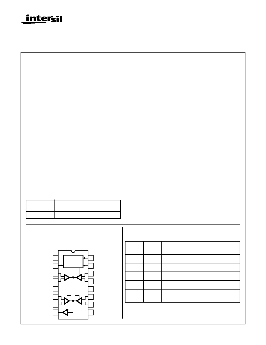
Pinout
HA-2444/883
(CERDIP)
TOP VIEW
1
2
3
4
5
7
6
8
GND
EN
+IN2
-IN2
V-
+IN1
OUT
-IN1
14
15
16
9
13
12
11
10
D1
+IN4
-IN4
V+
+IN3
-IN3
N/C
D0
DECODE
CONTROL
+
-
+
-
+
-
+
-
Logic Operation
TRUTH TABLE
EN
D1
D0
SELECTED
CHANNEL
H
L
L
1
H
L
H
2
H
H
L
3
H
H
H
4
L
X
X
NONE-OUT is set to a high
impedance state.
L = Low State (0.8V Max.)
H = High State (2.4V Min.)
X = Don't Care
Spec Number
511091-883
File Number
3608.1
3-2
Specifications HA-2444/883
Absolute Maximum Ratings
Thermal Information
Voltage between V+ and V- Terminals . . . . . . . . . . . . . . . . . . . . 35V
Differential Input Voltage . . . . . . . . . . . . . . . . . . . . . . . . . . . . . . . 6V
Voltage at Either Input Terminal . . . . . . . . . . . . . . . . . . . . . . V+ to V-
Voltage on Digital Inputs. . . . . . . . . . . . . . GND +7.5V to GND -0.5V
Peak Output Current (
10% Duty Cycle) . . . . . . . . . . . . . . . . . 40mA
Junction Temperature (T
J
) . . . . . . . . . . . . . . . . . . . . . . . . . . +175
o
C
Storage Temperature Range . . . . . . . . . . . . . . . . . -65
o
C to +150
o
C
ESD Rating. . . . . . . . . . . . . . . . . . . . . . . . . . . . . . . . . . . . . . <2000V
Lead Temperature (Soldering 10s) . . . . . . . . . . . . . . . . . . . . +300
o
C
Thermal Resistance
JA
JC
CerDIP Package . . . . . . . . . . . . . . . . . . .
82
o
C/W
27
o
C/W
Package Power Dissipation Limit at +75
o
C for T
J
+175
o
C
CerDIP Package . . . . . . . . . . . . . . . . . . . . . . . . . . . . . . . . . 1.22W
Package Power Dissipation Derating Factor Above +75
o
C
CerDIP Package . . . . . . . . . . . . . . . . . . . . . . . . . . . . . 12.2mW/
o
C
CAUTION: Stresses above those listed in "Absolute Maximum Ratings" may cause permanent damage to the device. This is a stress only rating and operation
of the device at these or any other conditions above those indicated in the operational sections of this specification is not implied.
Operating Conditions
Operating Temperature Range . . . . . . . . . . . . . . . . -55
o
C to +125
o
C
Operating Supply Voltage
. . . . . . . . . . . . . . . . . . . . . . . . . ±
12V to
±
15V
V
INCM
1/2(V+ - V-)
R
L
1k
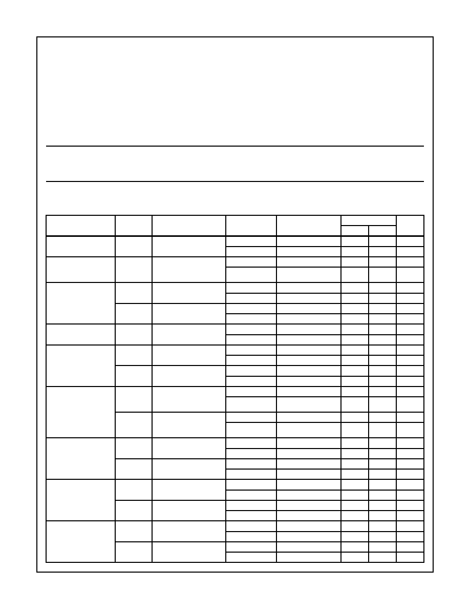
TABLE 1. DC ELECTRICAL PERFORMANCE CHARACTERISTICS
Device Tested at: V
SUPPLY
=
±
15V, R
SOURCE
= 50
, R
LOAD
= 1k
, C
LOAD
10pF, V
OUT
= 0V, V
IL
= 0.8V, V
IH
= 2.4V,
Unless Otherwise Specified.
PARAMETERS
SYMBOL
CONDITIONS
GROUP A
SUBGROUP
TEMPERATURE
LIMITS
UNITS
MIN
MAX
Input Offset Voltage
V
IO
V
CM
= 0V
1
+25
o
C
-7
7
mV
2, 3
+125
o
C, -55
o
C
-20
20
mV
Channel to Channel
Offset Voltage
Mismatch
V
IODEV
V
CM
= 0V
1
+25
o
C
-
5
mV
2, 3
+125
o
C, -55
o
C
-
12
mV
Input Bias Current
+I
B
V
CM
= 0V, +R
S
= 250
-R
S
= 50
1
+25
o
C
-15
15
µ
A
2, 3
+125
o
C, -55
o
C
-25
25
µ
A
-I
B
V
CM
= 0V, +R
S
= 50
-R
S
= 250
1
+25
o
C
-15
15
µ
A
2, 3
+125
o
C, -55
o
C
-25
25
µ
A
Input Offset Current
I
IO
V
CM
= 0V, +R
S
= 250
-R
S
= 250
1
+25
o
C
-4
4
µ
A
2, 3
+125
o
C, -55
o
C
-8
8
µ
A
Large Signal Voltage
Gain
+A
VOL
V
OUT
= 0V and +5V
4
+25
o
C
71
-
dB
5, 6
+125
o
C, -55
o
C
65
-
dB
-A
VOL
V
OUT
= 0V and -5V
4
+25
o
C
71
-
dB
5, 6
+125
o
C, -55
o
C
65
-
dB
Common Mode
Rejection Ratio
+CMRR
V
CM
= +5V,
V
OUT
= -5V,
V+ = 10V, V- = -20V
1
+25
o
C
68
-
dB
2, 3
+125
o
C, -55
o
C
68
-
dB
-CMRR
V
CM
= -5V,
V
OUT
= +5V,
V+ = 20V, V- = -10V
1
+25
o
C
68
-
dB
2, 3
+125
o
C, -55
o
C
68
-
dB
Output Voltage Swing
+V
OUT
1
+25
o
C
10
-
V
2, 3
+125
o
C, -55
o
C
10
-
V
-V
OUT
1
+25
o
C
-
-10
V
2, 3
+125
o
C, -55
o
C
-
-10
V
Output Current
+I
OUT
V
OUT
= -10V
R
LOAD
= OPEN
1
+25
o
C
25
-
mA
2, 3
+125
o
C, -55
o
C
25
-
mA
-I
OUT
V
OUT
= 10V
R
LOAD
= OPEN
1
+25
o
C
-
-25
mA
2, 3
+125
o
C, -55
o
C
-
-25
mA
Output Current
(Device Disabled)
+DISAB
V
OUT
= 5V, V
EN
= 0.8V
R
LOAD
= OPEN
1
+25
o
C
-
860
µ
A
2, 3
+125
o
C, -55
o
C
-
860
µ
A
-DISAB
V
OUT
= -5V, V
EN
= 0.8V
R
LOAD
= OPEN
1
+25
o
C
-
860
µ
A
2, 3
+125
o
C, -55
o
C
-
860
µ
A
Spec Number
511091-883
3-3
Specifications HA-2444/883
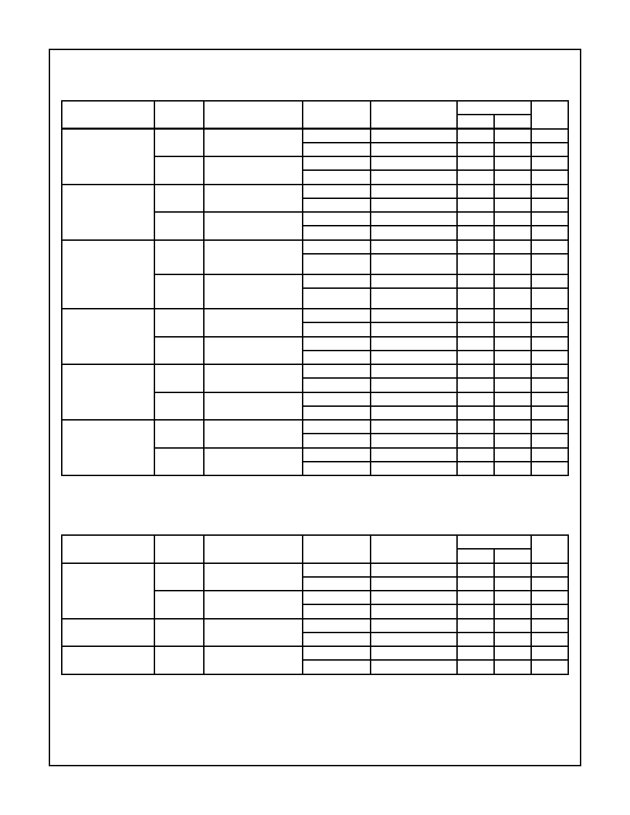
Quiescent Power
Supply Current
+I
CC
V
OUT
= 0V
I
OUT
= 0mA
1
+25
o
C
-
25
mA
2, 3
+125
o
C, -55
o
C
-
25
mA
-I
CC
V
OUT
= 0V
I
OUT
= 0mA
1
+25
o
C
-25
-
mA
2, 3
+125
o
C, -55
o
C
-25
-
mA
Supply Current
(Device Disabled)
+I
CCDIS
V
OUT
= 0V
V
EN
= 0.8V
1
+25
o
C
-
10
mA
2, 3
+125
o
C, -55
o
C
-
10
mA
-I
CCDIS
V
OUT
= 0V
V
EN
= 0.8V
1
+25
o
C
-10
-
mA
2, 3
+125
o
C, -55
o
C
-10
-
mA
Power Supply
Rejection
Ratio
+PSRR
V
SUPPLY
= 5V,
V+ = 15V, V- = -15V
V+ = 20V, V- = -15V
1
+25
o
C
65
-
dB
2, 3
+125
o
C, -55
o
C
65
-
dB
-PSRR
V
SUPPLY
= 5V,
V+ = 15V, V- = -15V
V+ = 15V, V- = -20V
1
+25
o
C
65
-
dB
2, 3
+125
o
C, -55
o
C
65
-
dB
Digital Input Voltages
(D0, D1, EN)
V
IL
1
+25
o
C
-
0.8
V
2, 3
+125
o
C, -55
o
C
-
0.8
V
V
IH
1
+25
o
C
2.4
-
V
2, 3
+125
o
C, -55
o
C
2.4
-
V
Input Current (D0, D1)
DX
IIL
V
IL
= 0V
1
+25
o
C
-
1
mA
2, 3
+125
o
C, -55
o
C
-
1
mA
DX
IIH
V
IH
= 5V
1
+25
o
C
-
1.2
µ
A
2, 3
+125
o
C, -55
o
C
-
1.2
µ
A
Input Current (EN)
EN
IIL
V
IL
= 0V
1
+25
o
C
-
50
µ
A
2, 3
+125
o
C, -55
o
C
-
50
µ
A
EN
IIH
V
IH
= 5V
1
+25
o
C
-
1.2
µ
A
2, 3
+125
o
C, -55
o
C
-
1.2
µ
A
TABLE 2. AC ELECTRICAL PERFORMANCE CHARACTERISTICS
Device Tested at: V
SUPPLY
=
±
15V, R
SOURCE
= 50
, R
LOAD
= 1k
, C
LOAD
10pF, A
VCL
= +1V/V, V
IL
= 0.8V, V
IH
= 2.4V,
Unless Otherwise Specified.
PARAMETERS
SYMBOL
CONDITIONS
GROUP A
SUBGROUP
TEMPERATURE
LIMITS
UNITS
MIN
MAX
Slew Rate
+SR
V
OUT
= -5V to +5V
7
+25
o
C
120
-
V/
µ
s
8
+125
o
C, -55
o
C
120
-
V/
µ
s
-SR
V
OUT
= +5V to -5V
7
+25
o
C
120
-
V/
µ
s
8
+125
o
C, -55
o
C
120
-
V/
µ
s
Channel Select
Time
CHSE
Note 1
V
EN
= 2.4V
9, 10
+25
o
C, +125
o
C
-
100
ns
11
-55
o
C
-
125
ns
Output Enable
Time
CHEN
Note 2
9
+25
o
C
-
100
ns
10, 11
+125
o
C, -55
o
C
-
100
ns
NOTES:
1. Measured for all channel combinations. Channel Select time is the delay in switching from channel X to channel Y. Channel Y input set
to +5V, all other channels set to 0V. Select time is measured from the 50% point of the critical digital select input to the 50% point on the
output.
2. Channel 1 selected with the input at 5V. All other channels set to 0V. Enable input switched from 0.8V to 2.4V. Enable time is measured
from the 50% point of the EN input to the 50% point on the output.
TABLE 1. DC ELECTRICAL PERFORMANCE CHARACTERISTICS
Device Tested at: V
SUPPLY
=
±
15V, R
SOURCE
= 50
, R
LOAD
= 1k
, C
LOAD
10pF, V
OUT
= 0V, V
IL
= 0.8V, V
IH
= 2.4V,
Unless Otherwise Specified. (Continued)
PARAMETERS
SYMBOL
CONDITIONS
GROUP A
SUBGROUP
TEMPERATURE
LIMITS
UNITS
MIN
MAX
Spec Number
511091-883

3-4
Specifications HA-2444/883
TABLE 3. ELECTRICAL PERFORMANCE CHARACTERISTICS
Device Characterized at: V
SUPPLY
=
±
15V, R
SOURCE
= 50
, R
LOAD
= 1k
, C
L
10pF, A
VCL
= 1V/V, V
IL
= 0.8V, V
IH
= 2.4V,
Unless Otherwise Specified.
PARAMETERS
SYMBOL
CONDITIONS
NOTES
TEMPERATURE
LIMITS
UNITS
MIN
MAX
Rise Time
T
R
V
OUT
= 0V to +200mV
1, 4
+25
o
C
-
11
ns
1, 4
-55
o
C, +125
o
C
-
12
ns
Fall Time
T
F
V
OUT
= 0V to -200mV
1, 4
+25
o
C
-
11
ns
1, 4
-55
o
C, +125
o
C
-
12
ns
Overshoot
+OS
V
OUT
= 0V to +200mV
1
+25
o
C
-
15
%
1
-55
o
C, +125
o
C
-
30
%
-OS
V
OUT
= 0V to -200mV
1
+25
o
C
-
15
%
1
-55
o
C, +125
o
C
-
30
%
Full Power Bandwidth
FPBW
V
PEAK
= 5V
1, 2
+25
o
C
3.8
-
MHz
1, 2
-55
o
C, +125
o
C
3.8
-
MHz
Minimum Closed Loop
Stable Gain
CLSG
1
+25
o
C
1
-
V/V
1
-55
o
C, +125
o
C
1
-
V/V
Quiescent Power
Consumption
PC
V
OUT
= 0V, I
OUT
= 0mA
1, 3
+25
o
C
-
750
mW
1, 3
-55
o
C, +125
o
C
-
750
mW
NOTES:
1. Parameters listed in Table 3 are controlled via design or process parameters and are not directly tested at final production. These param-
eters are lab characterized upon initial design release, or upon design changes. These parameters are guaranteed by characterization
based upon data from multiple production runs which reflect lot to lot and within lot variation.
2. Full Power Bandwidth guarantee based on Slew Rate measurement using FPBW = Slew Rate/(2
V
PEAK
).
3. Power Consumption based upon Quiescent Supply Current test maximum. (No load on outputs.)
4. Measured between 10% and 90% points.
TABLE 4. ELECTRICAL TEST REQUIREMENTS
MIL-STD-883 TEST REQUIREMENTS
SUBGROUPS (SEE TABLES 1 AND 2)
Interim Electrical Parameters (Pre Burn-In)
1
Final Electrical Test Parameters
1 (Note 1), 2, 3, 4, 5, 6, 7, 8, 9, 10, 11
Group A Test Requirements
1, 2, 3, 4, 5, 6, 7, 8, 9, 10, 11
Groups C and D Endpoints
1
NOTE:
1. PDA applies to Subgroup 1 only.
Spec Number
511091-883
3-5
HA-2444/883
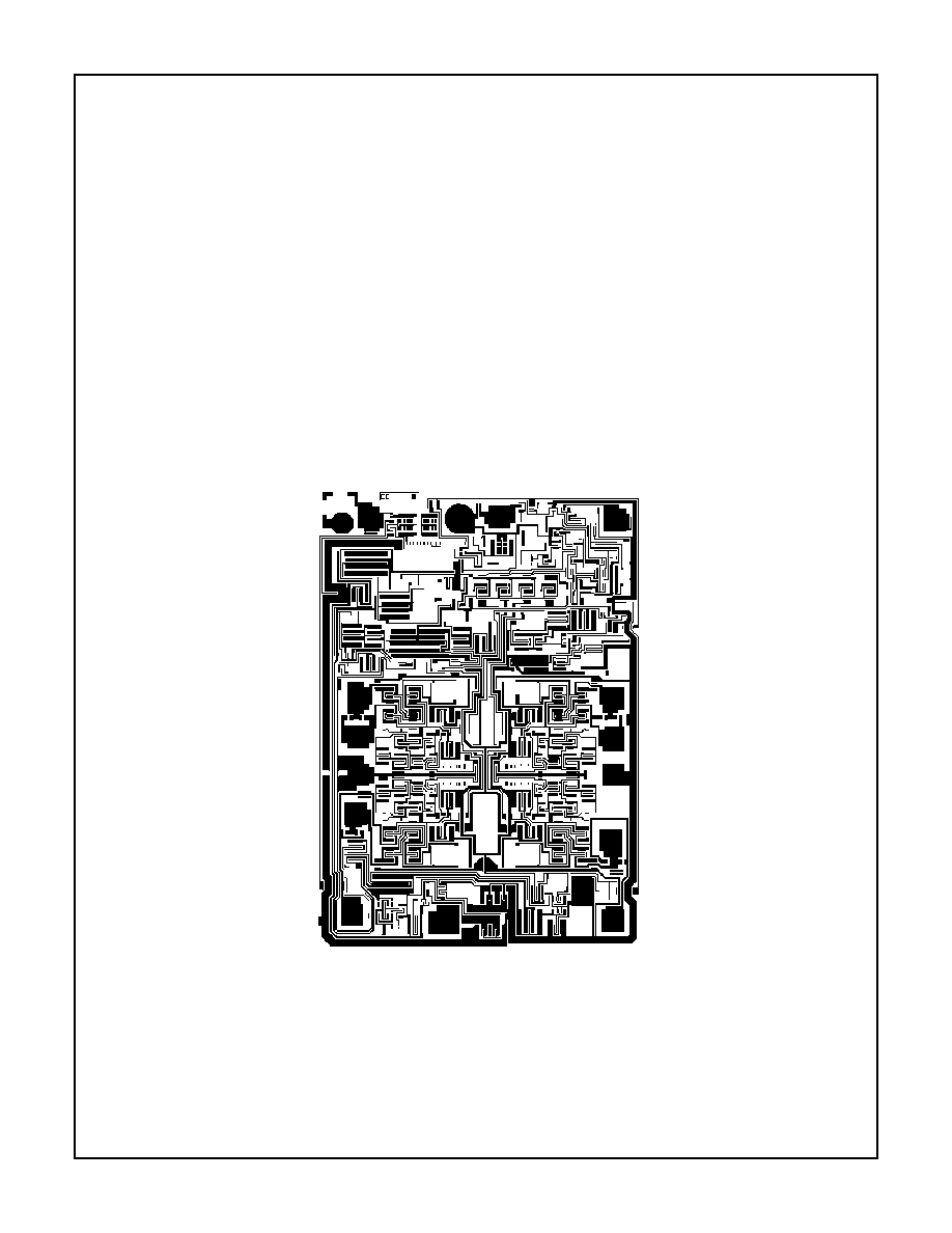
Die Characteristics
DIE DIMENSIONS:
74mils x 103mils x 19mils
±
1mil
1880
µ
m x 2620
µ
m x 483
µ
m
±
25.4
µ
m
METALLIZATION:
Type: Al, 1% Cu
Thickness: 16k
≈
±
2k
≈
SUBSTRATE POTENTIAL (Powered Up): V-
GLASSIVATION:
Type: Nitride over Silox
Silox Thickness: 12k
≈
±
2k
≈
Nitride Thickness: 3.5k
≈
±
1.5k
≈
TRANSISTOR COUNT: 129
PROCESS: Bipolar Dielectric Isolation
Metallization Mask Layout
HA-2444/883
4
2
1
8
7
6
5
+IN2
-IN2
D1
V+
OUT
D0
EN
GND
V-
+IN1
-IN1
-IN3
+IN3
-IN4
+IN4
Spec Number
511091-883
3-6
HA-2444/883
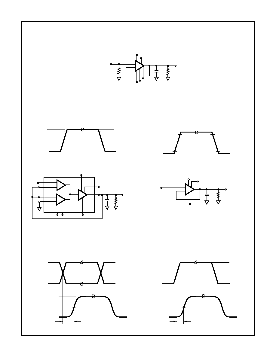
Test Waveforms
SIMPLIFIED TEST CIRCUIT FOR LARGE AND SMALL SIGNAL PULSE RESPONSE (Applies to Tables 2 and 3)
A
V
= +1 TEST CIRCUIT
LARGE SIGNAL WAVEFORM
SMALL SIGNAL WAVEFORM
SIMPLIFIED TEST CIRCUIT FOR CHANNEL SELECT TIMES
SIMPLIFIED TEST CIRCUIT FOR OUTPUT ENABLE TIMES
CHANNEL SELECT TIME SWITCHING WAVEFORMS
OUTPUT ENABLE TIME SWITCHING WAVEFORMS
-
+
V
IN
R
S
50
C
L
V
OUT
V+
V-
EN
+INX
-INX
D0
D1
1
k
NOTE:
1. V
S
=
±
15V, A
V
= +1, C
L
10pF
2. All 4 Channels Tested
3. D0 and D1 = 2.4V or 0.8V to Select Proper Channel
4. EN = 2.4V
+5V
-SR
+5V
+SR
V
OUT
-5V
-5V
10%
10%
90%
90%
90%
10%
90%
10%
0V
T
F
, -OS
+200mV
T
R
, +OS
V
OUT
0V
-200mV
+1
C
L
V
OUT
V+
EN
V-
1
k
+
-
-
+
+INY
-INY
+5V
-INX
+INX
+2.4V
D0
D1
NOTE:
1. V
S
=
±
15V, A
V
= +1 (all channels), C
L
10pF
2. All Channel Combinations Tested
-
+
+5V
C
L
V
OUT
V+
V-
+IN1
-IN1
EN
1
k
NOTE:
1. V
S
=
±
15V, A
V
= +1, C
L
10pF
2. D0 = D1 = 0.8V, +IN2 = +IN3 = +IN4 = 0V
50%
+2.4V
+2.4V
D0,D1
+0.8V
+0.8V
50%
tCHSE
+5V
+5V
0V
0V
VOUT
50%
+2.4V
+2.4V
+0.8V
+0.8V
50%
tCHEN
0V
0V
+5V
+5V
VOUT
EN
Spec Number
511091-883

3-7
All Intersil semiconductor products are manufactured, assembled and tested under ISO9000 quality systems certification.
Intersil products are sold by description only. Intersil Corporation reserves the right to make changes in circuit design and/or specifications at any time without
notice. Accordingly, the reader is cautioned to verify that data sheets are current before placing orders. Information furnished by Intersil is believed to be accurate
and reliable. However, no responsibility is assumed by Intersil or its subsidiaries for its use; nor for any infringements of patents or other rights of third parties which
may result from its use. No license is granted by implication or otherwise under any patent or patent rights of Intersil or its subsidiaries.
For information regarding Intersil Corporation and its products, see web site http://www.intersil.com
HA-2444/883