1
Æ
Features
∑ This Circuit is Processed in Accordance to MIL-STD-
883 and is Fully Conformant Under the Provisions of
Paragraph 1.2.1.
∑ High Slew Rate. . . . . . . . . . . . . . . . . . . . . . .25V/
µ
s (Min)
30V/
µ
s (Typ)
∑ Wide Power Bandwidth . . . . . . . . . . . . . . . 350kHz (Min)
∑ High Input Impedance . . . . . . . . . . . . . . . . . 25M
(Min)
50M
(Typ)
∑ Low Offset Current . . . . . . . . . . . . . . . . . . . 25nA (Max)
10nA (Typ)
∑ Low Quiescent Current . . . . . . . . . . . . . . . . . 6mA (Max)
∑ Fast Settling Time (0.1% of 10V Step) . . . . 330ns (Typ)
∑ High Gain Bandwidth Product . . . . . . . . . 12MHz (Typ)
∑ Internally Compensated For Unity Gain Stability
Applications
∑ Data Acquisition Systems
∑ RF Amplifiers
∑ Video Amplifiers
∑ Signal Generators
∑ Pulse Amplification
Description
HA-2500/883 is a monolithic operational amplifier which is
optimized to deliver excellent slew rate, bandwidth, and set-
tling time specifications. The outstanding dynamic features
of this internally compensated device are complemented
with low offset voltage and offset current.
This dielectrically isolated amplifier is ideally suited for appli-
cations such as data acquisition, RF, video, and pulse condi-
tioning circuits. Guaranteed slew rates of
±
25V/
µ
s minimum
make it an excellent component in fast, accurate data acqui-
sition and pulse amplification designs. To insure compliance,
all devices are 100% tested for AC performance characteris-
tics over the full temperature limits.
A typical 12MHz gain bandwidth product and 500kHz full
power bandwidth make this device well suited to RF and
video applications. With guaranteed offset voltages of 5mV
plus external offset adjust flexibility and low offset current,
this amplifier is particularly useful in signal conditioning
designs.
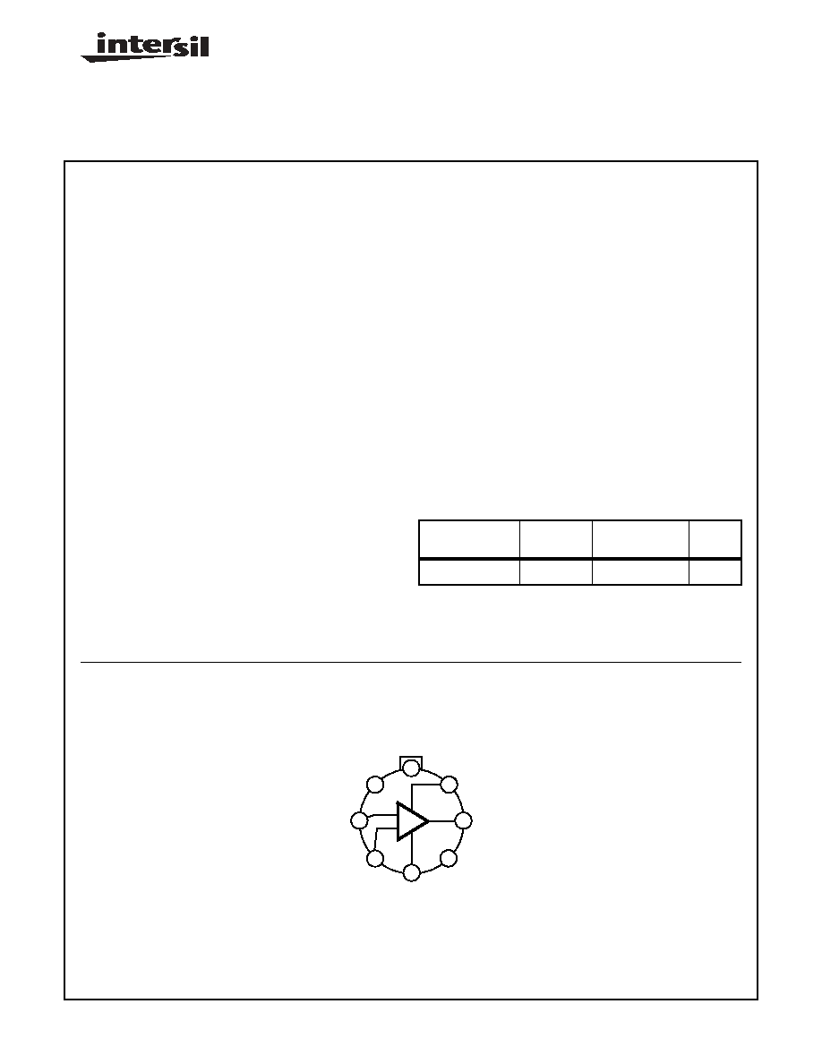
Pinout
Ordering Information
PART NUMBER
TEMP.
RANGE (
o
C)
PACKAGE
PKG.
NO.
HA2-2500/883
-55 to 125
8 Pin Can
T8.C
HA-2500/883
(METAL CAN)
TOP VIEW
2
4
6
1
3
7
5
8
COMP
OUT
-IN
V-
BAL
+IN
V+
BAL
+
-
April 2002
HA-2500/883
Precision High Slew Rate Operational Amplifier
Spec Number
511002-883
FN3734.2
CAUTION: These devices are sensitive to electrostatic discharge; follow proper IC Handling Procedures.
1-888-INTERSIL or 321-724-7143
|
Intersil (and design) is a registered trademark of Intersil Americas Inc.
Copyright © Intersil Americas Inc. 2002. All Rights Reserved
2
Absolute Maximum Ratings
Thermal Information
Voltage Between V+ and V- Terminals . . . . . . . . . . . . . . . . . . . 40V
Differential Input Voltage . . . . . . . . . . . . . . . . . . . . . . . . . . . . . . 15V
Voltage at Either Input Terminal . . . . . . . . . . . . . . . . . . . . . . V+ to V-
Peak Output Current . . . . . . . . . . . . . . . . . . . . . . . . . . . . . . . . 50mA
ESD Rating. . . . . . . . . . . . . . . . . . . . . . . . . . . . . . . . . . . . . . <2000V
Operating Conditions
Temperature Range . . . . . . . . . . . . . . . . . . . . . . . . . -55
o
C to 125
o
C
Supply Voltage
. . . . . . . . . . . . . . . . . . . . . . . . . . . . . . . . . . . . . . . . . ±
15V
V
INCM
1/2 (V+ - V-)
R
L
2k
Thermal Resistance (Typical, Note 1)
JA
JC
Metal Can Package . . . . . . . . . . . . . . . . . 160
o
C/W
75
o
C/W
Package Power Dissipation Limit at 75
o
C for T
J
175
o
C
Metal Can Package . . . . . . . . . . . . . . . . . . . . . . . . . . . . . . 625mW
Package Power Dissipation Derating Factor Above 75
o
C
Metal Can Package . . . . . . . . . . . . . . . . . . . . . . . . . . . . 6.3mW/
o
C
Maximum Junction Temperature. . . . . . . . . . . . . . . . . . . . . . . 175
o
C
Maximum Storage Temperature Range . . . . . . . . . .-65
o
C to 150
o
C
Maximum Lead Temperature (Soldering 10s). . . . . . . . . . . . . 300
o
C
CAUTION: Stresses above those listed in "Absolute Maximum Ratings" may cause permanent damage to the device. This is a stress only rating and operation
of the device at these or any other conditions above those indicated in the operational sections of this specification is not implied.
NOTE:
1.
JA
is measured with the component mounted on a low effective thermal conductivity test board in free air. See Tech Brief
TB379 for details.
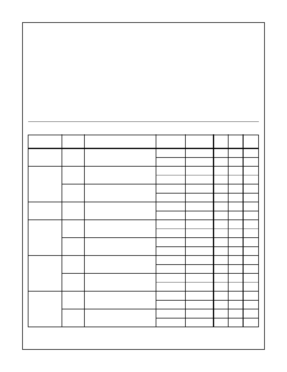
TABLE 1. DC ELECTRICAL PERFORMANCE CHARACTERISTICS
Device Tested at: V
SUPPLY
=
±
15V, R
SOURCE
= 100
, R
LOAD
= 500k
, V
OUT
= 0V, Unless Otherwise Specified.
PARAMETER
SYMBOL
CONDITIONS
GROUP A
SUBGROUPS
TEMP (
o
C)
MIN
MAX
UNITS
Input Offset
Voltage
V
IO
V
CM
= 0V
1
25
-5
5
mV
2, 3
125, -55
-8
8
mV
Input Bias Current
+I
B
V
CM
= 0V, +R
S
= 100k
, -R
S
= 100
1
25
-200
200
nA
2, 3
125, -55
-400
400
nA
-I
B
V
CM
= 0V, +R
S
= 100
, -R
S
= 100k
1
25
-200
200
nA
2, 3
125, -55
-400
400
nA
Input Offset
Current
I
IO
V
CM
= 0V,+R
S
= 100k
, -R
S
= 100k
1
25
-25
25
nA
2, 3
125, -55
-50
50
nA
Common Mode
Range
+CMR
V+ = 5V, V- = -25V
1
25
+10
-
V
2, 3
125, -55
+10
-
V
-CMR
V+ = 25V, V- = -5V
1
25
-
-10
V
2, 3
125, -55
-
-10
V
Large Signal
Voltage Gain
+A
VOL
V
OUT
= 0V and +10V, R
L
= 2k
4
25
20
-
kV/V
5, 6
125, -55
15
-
kV/V
-A
VOL
V
OUT
= 0V and -10V, R
L
= 2k
4
25
20
-
kV/V
5, 6
125, -55
15
-
kV/V
Common Mode
Rejection Ratio
+CMRR
V
CM
= +10V, V+ = +5V, V- = -25V,
V
OUT
= -10V
1
25
80
-
dB
2, 3
125, -55
80
-
dB
-CMRR
V
CM
= -10V, V+ = +25V, V- = -5V,
V
OUT
= +10V
1
25
80
-
dB
2, 3
125, -55
80
-
dB
HA-2500/883
Spec Number
511002-883
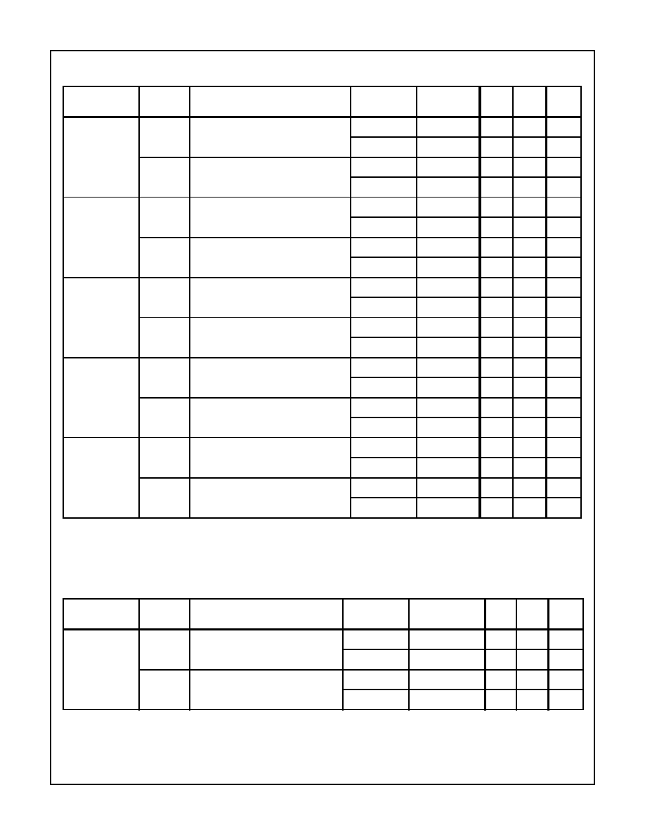
3
Output Voltage
Swing
+V
OUT
R
L
= 2k
4
25
10
-
V
5, 6
125, -55
10
-
V
-V
OUT
R
L
= 2k
4
25
-
-10
V
5, 6
125, -55
-
-10
V
Output Current
+I
OUT
V
OUT
= -10V
4
25
10
-
mA
5, 6
125, -55
7.5
-
mA
-I
OUT
V
OUT
= +10V
4
25
-
-10
mA
5, 6
125, -55
-
-7.5
mA
Quiescent Power
Supply Current
+I
CC
V
OUT
= 0V, I
OUT
= 0mA
1
25
-
6
mA
2, 3
125, -55
-
6.5
mA
-I
CC
V
OUT
= 0V, I
OUT
= 0mA
1
25
-6
-
mA
2, 3
125, -55
-6.5
-
mA
Power Supply
Rejection Ratio
+PSRR
V
SUP
= 10V, V+ = +20V, V- = -15V,
V+ = +10V, V- = -15V
1
25
80
-
dB
2, 3
125, -55
80
-
dB
-PSRR
V
SUP
= 10V, V+ = +15V, V- = -20V,
V+ = +15V, V- = -10V
1
25
80
-
dB
2, 3
125, -55
80
-
dB
Offset Voltage
Adjustment
+V
IO
Adj
Note 2
1
25
V
IO
-1
-
mV
2, 3
125, -55
V
IO
-1
-
mV
-V
IO
Adj
Note 2
1
25
V
IO
+1
-
mV
2, 3
125, -55
V
IO
+1
-
mV
NOTE:
2. Offset adjustment range is [V
IO
(Measured)
±
1mV] minimum referred to output. This test is for functionality only to assure adjustment
through 0V.
TABLE 2. ECTRICAL PERFORMANCE CHARACTERISTICS
Device Tested at: V
SUPPLY
=
±
15V, R
SOURCE
= 50
, R
LOAD
= 2k
, C
LOAD
= 50pF, A
VCL
= +1V/V, Unless Otherwise Specified.
PARAMETER
SYMBOL
CONDITIONS
GROUP A
SUBGROUPS
TEMP (
o
C)
MIN
MAX
UNITS
Slew Rate
+SR
V
OUT
= -5V to +5V, 25%
+SR
75%
7
25
25
-
V/
µ
s
8A, 8B
125, -55
20
-
V/
µ
s
-SR
V
OUT
= +5V to -5V, 75%
-SR
25%
7
25
25
-
V/
µ
s
8A, 8B
125, -55
20
-
V/
µ
s
TABLE 1. DC ELECTRICAL PERFORMANCE CHARACTERISTICS (Continued)
Device Tested at: V
SUPPLY
=
±
15V, R
SOURCE
= 100
, R
LOAD
= 500k
, V
OUT
= 0V, Unless Otherwise Specified.
PARAMETER
SYMBOL
CONDITIONS
GROUP A
SUBGROUPS
TEMP (
o
C)
MIN
MAX
UNITS
HA-2500/883
Spec Number
511002-883

4
Spec Number
511002-883
Rise and Fall
Time
t
r
V
OUT
= 0 to +200mV, 10%
t
r
90%
7
25
-
50
ns
8A, 8B
125, -55
-
60
ns
t
f
V
OUT
= 0 to -200mV, 10%
t
f
90%
7
25
-
50
ns
8A, 8B
125, -55
-
60
ns
Overshoot
+OS
V
OUT
= 0 to +200mV
7
25
-
40
%
8A, 8B
125, -55
-
50
%
-OS
V
OUT
= 0 to -200mV
7
25
-
40
%
8A, 8B
125, -55
-
50
%
TABLE 3. ELECTRICAL PERFORMANCE CHARACTERISTICS
Device Characterized at: V
SUPPLY
=
±
15V, R
LOAD
= 2k
, C
LOAD
= 50pF, Unless Otherwise Specified.
PARAMETER
SYMBOL
CONDITIONS
NOTES
TEMP (
o
C)
MIN
MAX
UNITS
Differential Input
Resistance
R
IN
V
CM
= 0V
3
25
25
-
M
Full Power
Bandwidth
FPBW
V
PEAK
= 10V
3, 4
25
350
-
kHz
Minimum Closed
Loop Stable Gain
CLSG
R
L
= 2k
, C
L
= 50pF
3
-55 to 125
1
-
V/V
Quiescent Power
Consumption
PC
V
OUT
= 0V, I
OUT
= 0mA
3, 5
-55 to 125
-
195
mW
NOTES:
3. Parameters listed in Table 3 are controlled via design or process parameters and are not directly tested at final production. These param-
eters are lab characterized upon initial design release, or upon design changes. These parameters are guaranteed by characterization
based upon data from multiple production runs which reflect lot to lot and within lot variation.
4. Full Power Bandwidth guarantee based on Slew Rate measurement using FPBW = Slew Rate/(2
V
PEAK
).
5. Quiescent Power Consumption based upon Quiescent Supply Current test maximum. (No load on outputs.)
TABLE 4. ELECTRICAL TEST REQUIREMENTS
MIL-STD-883 TEST REQUIREMENTS
SUBGROUPS (SEE TABLES 1 AND 2)
Interim Electrical Parameters (Pre Burn-In)
1
Final Electrical Test Parameters
1 (Note 6), 2, 3, 4, 5, 6, 7, 8A, 8B
Group A Test Requirements
1, 2, 3, 4, 5, 6, 7, 8A, 8B
Groups C and D Endpoints
1
NOTE:
6. PDA applies to Subgroup 1 only.
TABLE 2. ECTRICAL PERFORMANCE CHARACTERISTICS (Continued)
Device Tested at: V
SUPPLY
=
±
15V, R
SOURCE
= 50
, R
LOAD
= 2k
, C
LOAD
= 50pF, A
VCL
= +1V/V, Unless Otherwise Specified.
PARAMETER
SYMBOL
CONDITIONS
GROUP A
SUBGROUPS
TEMP (
o
C)
MIN
MAX
UNITS
HA-2500/883
5
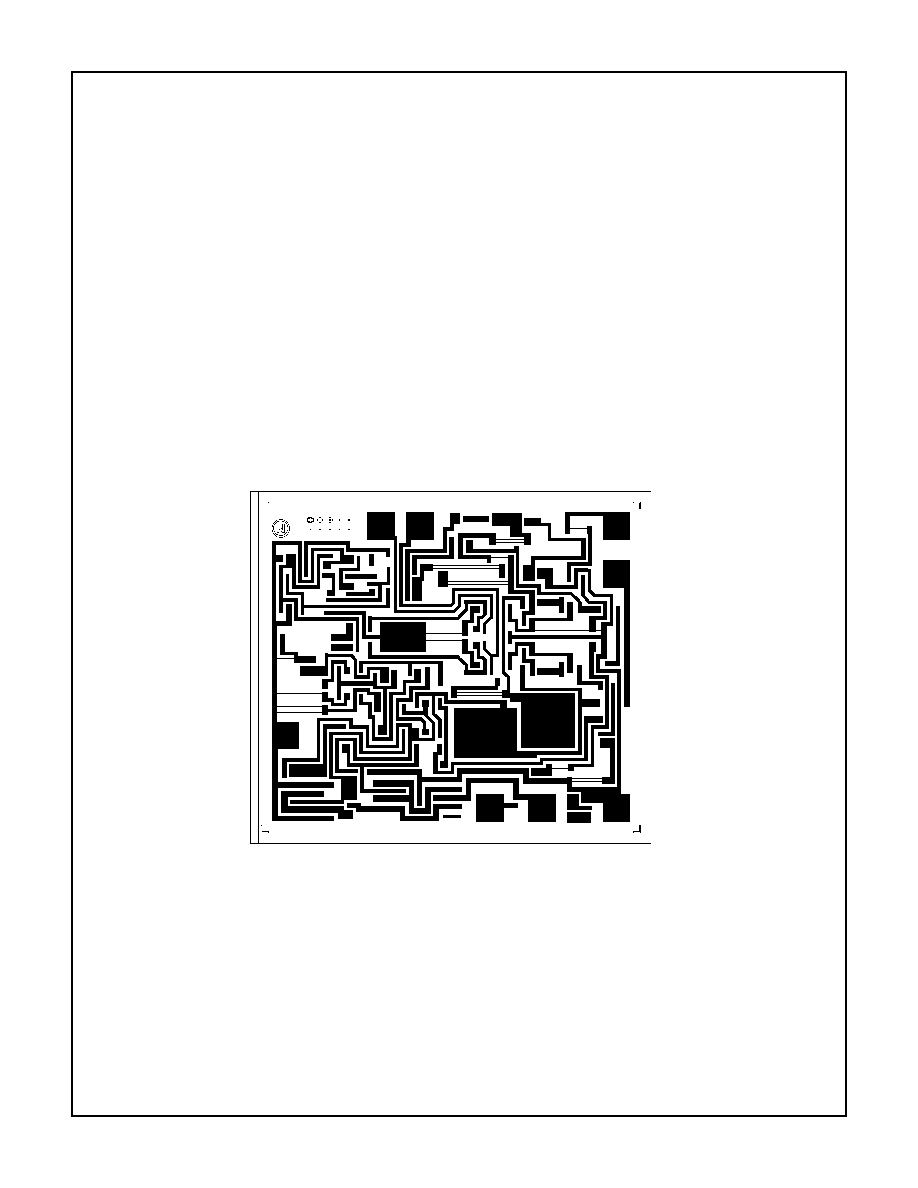
Die Characteristics
DIE DIMENSIONS:
57 x 65 x 19 milss
1450 x 1650
x 483
µ
m
METALLIZATION:
Type: Al, 1% Cu
Thickness: 16k
≈
±
2k
≈
GLASSIVATION:
Type: Nitride (Si3N4) over Silox (SiO2, 5% Phos.)
Silox Thickness: 12k≈
±
2k≈
Nitride Thickness: 3.5k≈
±
1.5k≈
WORST CASE CURRENT DENSITY:
0.3 x 10
5
A/cm
2
SUBSTRATE POTENTIAL (Powered Up):
Unbiased
TRANSISTOR COUNT:
HA-2500/883: 40
PROCESS: Bipolar Dielectric Isolation
Metallization Mask Layout
HA-2500/883
V+
OUT
BAL
V-
BAL
-IN
+IN
COMP
HA-2500/883
Spec Number
511002-883

6
Spec Number
511002-883
Burn-In Circuits
HA2-2500/883 METAL CAN
NOTES:
R
1
= 1M
,
±
5%, 1/4W (Min)
C
1
= C
2
= 0.01
µ
F/Socket (Min) or 0.1
µ
F/Row (Min)
C
3
= 0.01
µ
F/Socket (10%)
D
1
= D
2
= 1N4002 or Equivalent/Board
|(V+) - (V-)| = 30V
1
5
8
+
-
V+
C
1
D
1
6
2
7
C
3
3
R
1
4
C
2
D
2
V-
HA-2500/883

7
All Intersil U.S. products are manufactured, assembled and tested utilizing ISO9000 quality systems.
Intersil Corporation's quality certifications can be viewed at www.intersil.com/design/quality
Intersil products are sold by description only. Intersil Corporation reserves the right to make changes in circuit design, software and/or specifications at any time without
notice. Accordingly, the reader is cautioned to verify that data sheets are current before placing orders. Information furnished by Intersil is believed to be accurate and
reliable. However, no responsibility is assumed by Intersil or its subsidiaries for its use; nor for any infringements of patents or other rights of third parties which may result
from its use. No license is granted by implication or otherwise under any patent or patent rights of Intersil or its subsidiaries.
For information regarding Intersil Corporation and its products, see www.intersil.com
Sales Office Headquarters
NORTH AMERICA
Intersil Corporation
7585 Irvine Center Drive
Suite 100
Irvine, CA 92618
TEL: (949) 341-7000
FAX: (949) 341-7123
Intersil Corporation
2401 Palm Bay Rd.
Palm Bay, FL 32905
TEL: (321) 724-7000
FAX: (321) 724-7946
EUROPE
Intersil Europe Sarl
Ave. William Graisse, 3
1006 Lausanne
Switzerland
TEL: +41 21 6140560
FAX: +41 21 6140579
ASIA
Intersil Corporation
Unit 1804 18/F Guangdong Water Building
83 Austin Road
TST, Kowloon Hong Kong
TEL: +852 2723 6339
FAX: +852 2730 1433
HA-2500/883
Spec Number
511002-883
Metal Can Packages (Can)
NOTES:
1. (All leads) ÿb applies between L1 and L2. ÿb1 applies between
L2 and 0.500 from the reference plane. Diameter is uncontrolled
in L1 and beyond 0.500 from the reference plane.
2. Measured from maximum diameter of the product.
3.
is the basic spacing from the centerline of the tab to terminal 1
and
is the basic spacing of each lead or lead position (N -1
places) from
,
looking at the bottom of the package.
4. N is the maximum number of terminal positions.
5. Dimensioning and tolerancing per ANSI Y14.5M - 1982.
6. Controlling dimension: INCH.
ÿb
ÿD2
ÿ
e
k1
k
ÿb1
BASE AND
SEATING PLANE
F
Q
ÿD ÿD1
L1
L2
REFERENCE PLANE
L
A
ÿb2
ÿb1
BASE METAL
LEAD FINISH
SECTION A-A
A
A
N
e
1
CL
2
1
T8.C
MIL-STD-1835 MACY1-X8 (A1)
8 LEAD METAL CAN PACKAGE
SYMBOL
INCHES
MILLIMETERS
NOTES
MIN
MAX
MIN
MAX
A
0.165
0.185
4.19
4.70
-
ÿb
0.016
0.019
0.41
0.48
1
ÿb1
0.016
0.021
0.41
0.53
1
ÿb2
0.016
0.024
0.41
0.61
-
ÿD
0.335
0.375
8.51
9.40
-
ÿD1
0.305
0.335
7.75
8.51
-
ÿD2
0.110
0.160
2.79
4.06
-
e
0.200 BSC
5.08 BSC
-
e1
0.100 BSC
2.54 BSC
-
F
-
0.040
-
1.02
-
k
0.027
0.034
0.69
0.86
-
k1
0.027 0.045
0.69
1.14
2
L
0.500
0.750
12.70
19.05
1
L1
-
0.050
-
1.27
1
L2
0.250
-
6.35
-
1
Q
0.010
0.045
0.25
1.14
-
45
o
BSC
45
o
BSC
3
45
o
BSC
45
o
BSC
3
N
8
8
4
Rev. 0 5/18/94