1
CAUTION: These devices are sensitive to electrostatic discharge; follow proper IC Handling Procedures.
1-888-INTERSIL or 321-724-7143
|
Copyright
©
Intersil Corporation 1999
HA-5033
250MHz Video Buffer
The HA-5033 is a unity gain monolithic IC designed for any
application requiring a fast, wideband buffer. Featuring a
bandwidth of 250MHz and outstanding differential phase/
gain characteristics, this high performance voltage follower is
an excellent choice for video circuit design. Other features,
which include a minimum slew rate of 1000V/
µ
s and high
output drive capability, make the HA-5033 applicable for line
driver and high speed data conversion circuits.
The high performance of this product is a result of the Intersil
Dielectric Isolation process. A major feature of this process
is that it produces both PNP and NPN high frequency
transistors which makes wide bandwidth designs, such as
the HA-5033, practical. Alternative process methods
typically produce a lower AC performance.
Features
∑ Differential Phase Error . . . . . . . . . . . . . . . 0.02 Degrees
∑ Differential Gain Error. . . . . . . . . . . . . . . . . . . . . . . 0.03%
∑ High Slew Rate. . . . . . . . . . . . . . . . . . . . . . . . . . 1100V/
µ
s
∑ Wide Bandwidth (Small Signal) . . . . . . . . . . . . . . 250MHz
∑ Wide Power Bandwidth . . . . . . . . . . . . . . DC to 17.5MHz
∑ Fast Rise Time . . . . . . . . . . . . . . . . . . . . . . . . . . . . . . 3ns
∑ High Output Drive . . . . . . . . . . . . . .
±
10V With 100
Load
∑ Wide Power Supply Range. . . . . . . . . . . . . .
±
5V to
±
16V
∑ Replace Costly Hybrids
Applications
∑ Video Buffer
∑ High Frequency Buffer
∑ Isolation Buffer
∑ High Speed Line Driver
∑ Impedance Matching
∑ Current Boosters
∑ High Speed A/D Input Buffers
∑ Related Literature
- AN548, Designer's Guide for HA-5033
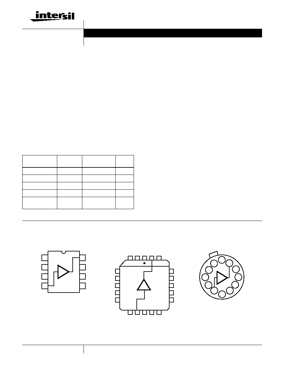
Pinouts
Ordering Information
PART NUMBER
(BRAND)
TEMP.
RANGE (
o
C)
PACKAGE
PKG.
NO.
HA2-5033-2
-55 to 125
12 Pin Metal Can
T12.C
HA2-5033-5
0 to 75
12 Pin Metal Can
T12.C
HA3-5033-5
0 to 75
8 Ld PDIP
E8.3
HA4P5033-5
0 to 75
20 Ld PLCC
N20.35
HA9P5033-5
(H50335)
0 to 60
(Note 3)
8 Ld PSOP
M8.15A
HA-5033
(PDIP, PSOP)
TOP VIEW
HA-5033
(PLCC)
TOP VIEW
HA-5033
(METAL CAN)
TOP VIEW
1
2
3
4
8
7
6
5
OUT
NC
SUB-
V-
V+
NC
NC
IN
STRATE
19
3
2
20
1
15
16
17
18
14
9
10
11
12
13
4
5
6
7
8
NC
NC
NC
NC
NC
NC
IN
NC
V-
NC
NC
NC
V+
NC
OUT
NC
NC
NC
NC
SUB-
STRATE
CASE
NC
12
1
2
3
4
11
10
9
8
7
6
5
V+
OUT
V-
NC
NC
NC
+IN
NC
NC
NC
Data Sheet
September 1998
File Number
2924.4
2
Absolute Maximum Ratings
Thermal Information
Voltage Between V+ and V- Pins . . . . . . . . . . . . . . . . . . . . . . . . 40V
DC Input Voltage . . . . . . . . . . . . . . . . . . . . . . . . . . . . . . . . . V+ to V-
Output Current (Peak) (50ms On/1 Second Off) . . . . . . . . .
±
200mA
ESD Rating
Human Body Model (Per MIL-STD-883 Method 3015.7) . . . . 2000V
Operating Conditions
Temperature Ranges
HA-5033-2 . . . . . . . . . . . . . . . . . . . . . . . . . . . . . . -55
o
C to 125
o
C
HA-5033-5 (Note 3) . . . . . . . . . . . . . . . . . . . . . . . . . 0
o
C to 75
o
C
HA9P5033-5 (Notes 1, 3) . . . . . . . . . . . . . . . . . . . . -40
o
C to 60
o
C
Thermal Resistance (Typical, Note 2)
JA
(
o
C/W)
JC
(
o
C/W)
Metal Can Package . . . . . . . . . . . . . . .
65
34
PDIP Package . . . . . . . . . . . . . . . . . . .
96
N/A
PSOP Package (Note 4) . . . . . . . . . . .
129
N/A
PLCC Package . . . . . . . . . . . . . . . . . . .
80
N/A
Maximum Junction Temperature (Note 1) . . . . . . . . . . . . . . . . .175
o
C
Maximum Junction Temperature (Plastic Packages) . . . . . . .150
o
C
Maximum Storage Temperature Range . . . . . . . . . . -65
o
C to 150
o
C
Maximum Lead Temperature (Soldering 10s) . . . . . . . . . . . . 300
o
C
(PSOP and PLCC - Lead Tips Only)
CAUTION: Stresses above those listed in "Absolute Maximum Ratings" may cause permanent damage to the device. This is a stress only rating and operation of the
device at these or any other conditions above those indicated in the operational sections of this specification is not implied.
NOTES:
1. Maximum power dissipation, including load conditions, must be designed to maintain the maximum junction temperature below 175
o
C for the metal
can package, and below 150
o
C for the plastic packages (See Figure 5.).
2.
JA
is measured with the component mounted on an evaluation PC board in free air.
3. Maximum operating temperature in the PSOP package is limited to 60
o
C, for V
SUPPLY
=
±
12V to prevent the junction temperature from exceed-
ing 150
o
C. The maximum operating temperature may have to be derated further, depending on the output load condition. The operating tem-
perature may be increased if the HA9P5033 is operated at lower V
SUPPLY
. For example, the quiescent operating temperature may be increased
to 75
o
C by operating at V
SUPPLY
±
9.7V. See Figure 5 for more information.
4. Direct attach of the PSOP copper slug to copper area on the PCB can reduce the
JA
value to <100
o
C/W. Consult the Intersil Application Group
for more information.
Electrical Specifications
V
SUPPLY
=
±
12V, R
S
= 50
, R
L
= 100
,
C
L
= 10pF, Unless Otherwise Specified
PARAMETER
TEST
CONDITIONS
TEMP.
(
o
C)
HA-5033-2
HA-5033-5
UNITS
MIN
TYP
MAX
MIN
TYP
MAX
INPUT CHARACTERISTICS
Offset Voltage
25
-
5
15
-
5
15
mV
Full
-
6
25
-
6
25
mV
Average Offset Voltage Drift
Full
-
33
-
-
33
-
µ
V/
o
C
Bias Current
25
-
20
35
-
20
35
µ
A
Full
-
30
50
-
30
50
µ
A
Input Resistance
25
-
3
-
-
3
-
M
Input Capacitance
25
-
1.6
-
-
1.6
-
pF
Input Noise Voltage
10Hz to 100MHz
25
-
20
-
-
20
-
µ
V
P-P
TRANSFER CHARACTERISTICS
Voltage Gain
R
L
= 100
25
0.93
-
-
0.93
-
-
V/V
R
L
= 1k
25
0.93
0.99
-
0.93
0.99
-
V/V
R
L
= 100
Full
0.92
-
-
0.92
-
-
V/V
-3dB Bandwidth
25
-
250
-
-
250
-
MHz
OUTPUT CHARACTERISTICS
Output Voltage Swing
R
L
= 100
Full
±
8
±
10
-
±
8
±
10
-
V
R
L
= 1k
, V
S
=
±
15V
Full
±
11
±
12
-
±
11
±
12
-
V
Output Current
25
±
80
±
100
-
±
80
±
100
-
mA
Output Resistance
25
-
8
-
-
8
-
Full Power Bandwidth
V
OUT
= 1V
RMS
, R
L
= 1k
25
-
146
-
-
146
-
MHz
Full Power Bandwidth (Note 5)
25
15.9
17.5
-
15.9
17.5
-
MHz
TRANSIENT RESPONSE
Rise Time
V
OUT
= 500mV
25
-
4.6
-
-
4.6
-
ns
Propagation Delay
25
-
1
-
-
1
-
ns
Overshoot
25
-
3
-
-
3
-
%
Slew Rate (Note 5)
25
1
1.1
-
1
1.1
-
V/ns
HA-5033
3
Settling Time to 0.1%
25
-
50
-
-
50
-
ns
Differential Phase Error (Note 6)
25
-
0.02
-
-
0.02
-
Degree
Differential Gain Error (Note 6)
25
-
0.03
-
-
0.03
-
%
POWER SUPPLY CHARACTERISTICS
Supply Current
25
-
21
25
-
21
25
mA
Full
-
21
30
-
21
30
mA
Power Supply Rejection Ratio
Full
54
-
-
54
-
-
dB
Harmonic Distortion
V
IN
= 1V
RMS
at 100kHz
25
-
<0.1
-
-
<0.1
-
%
NOTES:
5. V
SUPPLY
=
±
15V, V
OUT
=
±
10V, R
L
= 1k
.
6. Differential gain and phase error are nonlinear signal distortions found in video systems and are defined as follows: Differential gain error is
defined as the change in amplitude at the color subcarrier frequency as the picture signal is varied from blanking to white level. Differential phase
error is defined as the change in the phase of the color subcarrier as the picture signal is varied from blanking to white level. R
L
= 300
.
Electrical Specifications
V
SUPPLY
=
±
12V, R
S
= 50
, R
L
= 100
,
C
L
= 10pF, Unless Otherwise Specified (Continued)
PARAMETER
TEST
CONDITIONS
TEMP.
(
o
C)
HA-5033-2
HA-5033-5
UNITS
MIN
TYP
MAX
MIN
TYP
MAX
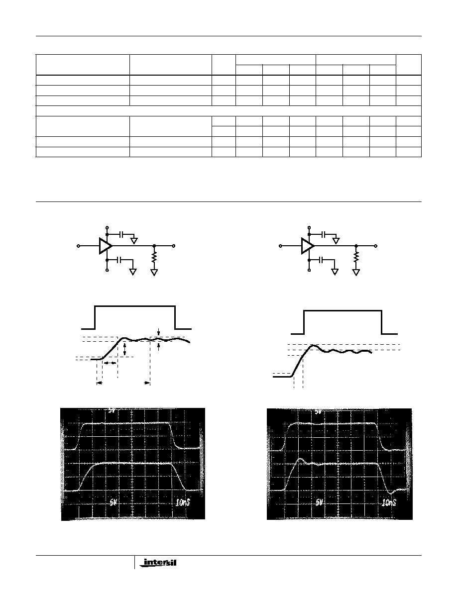
Test Circuits and Waveforms
FIGURE 1. SLEW RATE AND SETTLING TIME
FIGURE 2. TRANSIENT RESPONSE
FIGURE 3. SETTLING TIME AND SLEW RATE
FIGURE 4. RISE TIME AND OVERSHOOT
+10V RESPONSE
+10V RESPONSE
+15V
R
L
OUT
IN
0.1
µ
F
0.1
µ
F
-15V
+12V
100
OUT
IN
0.1
µ
F
0.1
µ
F
-12V
10V
INPUT
90%
OUTPUT
10%
ERROR BAND
±
10mV FROM
FINAL VALUE
SLEW
V/
t
0V
V
RATE =
t
SETTLING TIME
INPUT
90%
OUTPUT
10%
0V
500mV
OVERSHOOT
NOTE: Measured on both
positive and negative transitions.
V
OUT
V
IN
0V
0V
T
A
= 25
o
C, R
S
= 50
,
R
L
= 100
V
OUT
V
IN
0V
0V
T
A
= 25
o
C, R
S
= 50
,
R
L
= 1k
HA-5033

4
Schematic Diagram
Application Information
Layout Considerations
The wide bandwidth of the HA-5033 necessitates that high
frequency circuit layout procedures be followed. Failure to
follow these guidelines can result in marginal performance.
Probably the most crucial of the RF/video layout rules is the
use of a ground plane. A ground plane provides isolation and
minimizes distributed circuit capacitance and inductance
which will degrade high frequency performance. This ground
plane shielding can also incorporate the metal case of the
HA-5033 since pin #2 is internally tied to the package. This
feature allows the user to make metal to metal contact
between the ground plane and the package, which extends
shielding, provides additional heat sinking and eliminates the
use of a socket, IC sockets contribute inter-lead capacitance
which limits device bandwidth and should be avoided.
For the PDIP, pin 6 can be tied to either supply, grounded, or
simply not used. But to optimize device performance and
improve isolation, it is recommended that this pin be grounded.
Other considerations are proper power supply bypassing
and keeping the input and output connections as short as
possible which minimizes distributed capacitance and
reduces board space.
Power Supply Decoupling
For optimum device performance, it is recommended that
the positive and negative power supplies be bypassed with
capacitors to ground. Ceramic capacitors ranging in value
from 0.01
µ
F to 0.1
µ
F will minimize high frequency variations
in supply voltage. Solid tantalum capacitors 1
µ
F or larger will
optimize low frequency performance.
T
A
= 25
o
C, R
S
= 50
,
R
L
= 100
PULSE RESPONSE
Test Circuits and Waveforms
(Continued)
V
OUT
V
IN
0V
0V
500mV
500mV
R
4
Q
15
Q
16
Q
19
R
6
Q
17
V+
Q
18
R
3
Q
13
Q
14
Q
12
Q
11
Q
3
Q
5
V
IN
R
5
V-
R
8
Q
4
R
9
Q
6
R
2
Q
10
Q
7
Q
8
R
1
R
13
Q
9
Q
2
R
10
R
11
Q
1
R
12
V
OUT
HA-5033
5
It is also recommended that the bypass capacitors be
connected close to the HA-5033 (preferably directly to the
supply pins).
Figure 5 is based on:
Where: T
JMAX
= Maximum Junction Temperature of the Device
T
A
= Ambient Temperature
JA
= Junction to Ambient Thermal Resistance
P
DMAX
T
JMAX
T
A
≠
JA
-------------------------------
=
MAXIMUM T
O
T
AL PO
WER DISSIP
A
TION (W)
PDIP
PSOP
CAN
QUIESCENT P
D
= 0.72W
AT V
S
=
±
12V, I
CC
= 30mA
0.6
0.4
0.2
0
25
45
65
85
105
125
TEMPERATURE (
o
C)
0.8
1.0
1.2
1.4
1.6
1.8
2.0
2.2
2.4
FIGURE 5. MAXIMUM POWER DISSIPATION vs
TEMPERATURE
PLCC
Typical Applications
(Also see Application Note AN548)
FIGURE 6. VIDEO COAXIAL LINE DRIVER 50
SYSTEM
FIGURE 7. VIDEO GAIN BLOCK
POSITIVE PULSE RESPONSE
NEGATIVE PULSE RESPONSE
R
L
RG -58
50
R
M
R
S
-12V
+12V
V
IN
5
12
10
0.1
µ
F
0.1
µ
F
11
50
75
VIDEO
75
OUTPUT
HA-5033
900
V-
V+
HA-2539
V-
V+
100
15
60
R
2
R
1
VIDEO
SIGNAL
INPUT
+
-
V
OUT
V
IN
0V
0V
T
A
= 25
o
C, R
S
= 50
, R
M
= R
L
= 50
V
O
V
IN
R
L
R
L
R
M
+
----------------------
1
2
---
V
IN
=
=
V
OUT
V
IN
0V
0V
T
A
= 25
o
C, R
S
= 50
, R
M
= R
L
= 50
V
O
V
IN
R
L
R
L
R
M
+
----------------------
1
2
---
V
IN
=
=
HA-5033
6
Typical Performance Curves
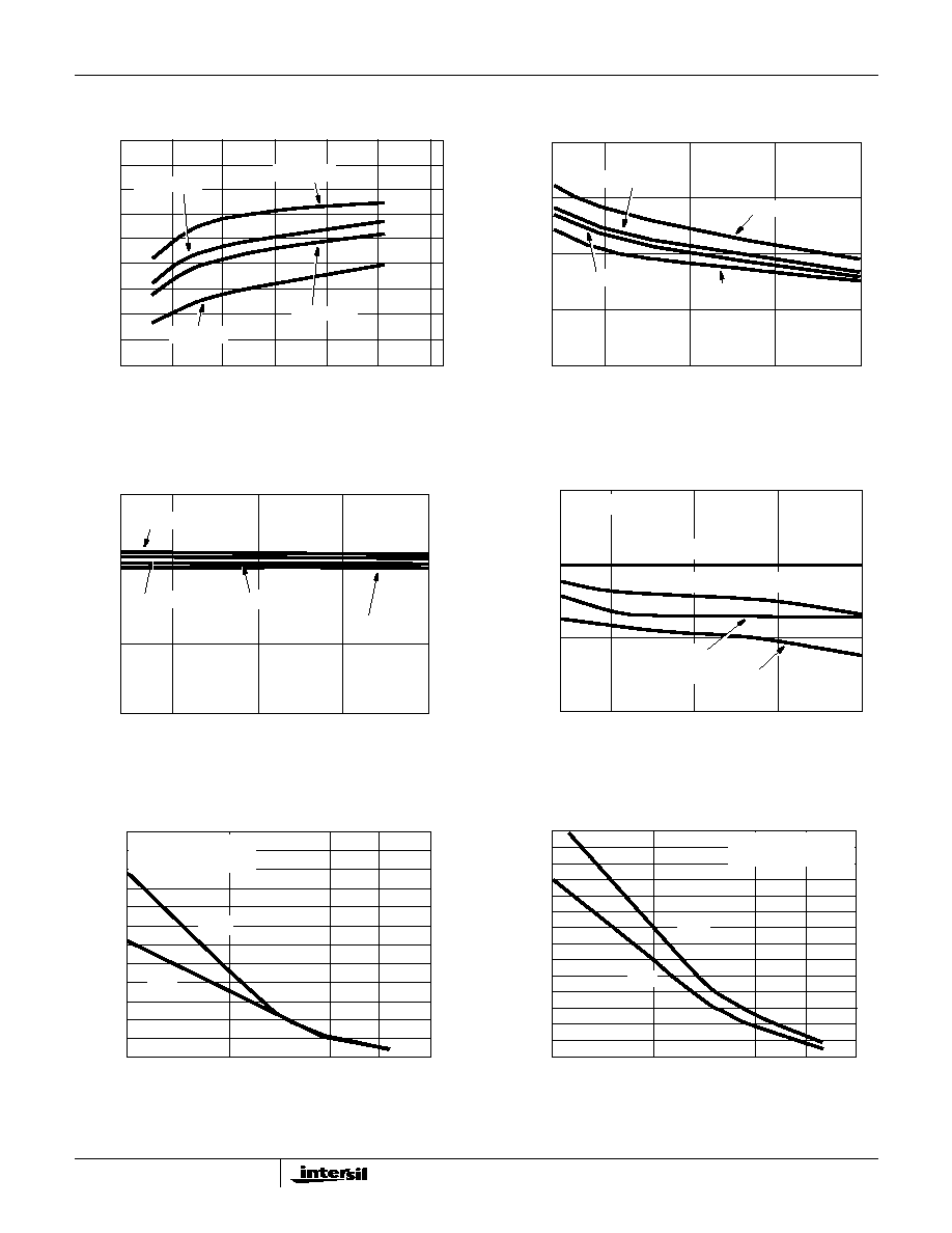
FIGURE 8. INPUT OFFSET VOLTAGE vs TEMPERATURE
FIGURE 9. INPUT BIAS CURRENT vs TEMPERATURE
FIGURE 10. SUPPLY CURRENT vs TEMPERATURE
FIGURE 11. SLEW RATE vs TEMPERATURE
FIGURE 12. SLEW RATE vs LOAD CAPACITANCE
FIGURE 13. SLEW RATE vs LOAD CAPACITANCE
8
7
6
5
4
-80
40
160
TEMPERATURE (
o
C)
OFFSET V
O
L
T
A
GE (mV)
3
2
1
120
80
-40
0
V
S
=
±
12V
V
S
=
±
15V
V
S
=
±
10V
V
S
=
±
5V
40
30
20
-55
75
125
TEMPERATURE (
o
C)
INPUT BIAS CURRENT (
µ
A)
10
0
-25
25
V
S
=
±
15V
V
S
=
±
12V
V
S
=
±
5V
V
S
=
±
10V
30
20
10
0
-55
25
125
TEMPERATURE (
o
C)
SUPPL
Y CURRENT (mA)
75
-25
V
S
=
±
15V
V
S
=
±
12V
V
S
=
±
10V
V
S
=
±
5V
TEMPERATURE (
o
C)
3000
2000
1000
SLEW RA
TE (V/
µ
s)
V
S
=
±
15V, V
IN
=
±
10V
-55
75
125
-25
25
FALL (R
L
= 1k
)
FALL (R
L
= 100
)
RISE (R
L
= 1k
)
RISE (R
L
= 100
)
CAPACITANCE (pF)
5000
10,000
1000
100
0
SLEW RA
TE (V/
µ
s)
2400
2200
2000
1800
200
400
600
800
1000
1200
1400
1600
V
S
=
±
15V, R
L
= 1k
T
A
= 25
o
C, V
IN
=
±
10V
FALL
RISE
CAPACITANCE (pF)
5000
10,000
1000
100
0
SLEW RA
TE (V/
µ
s)
1400
1300
1200
1100
200
400
500
600
700
800
900
1000
100
V
S
=
±
15V, R
L
= 100
T
A
= 25
o
C, V
IN
=
±
10V
FALL
RISE
300
HA-5033
7
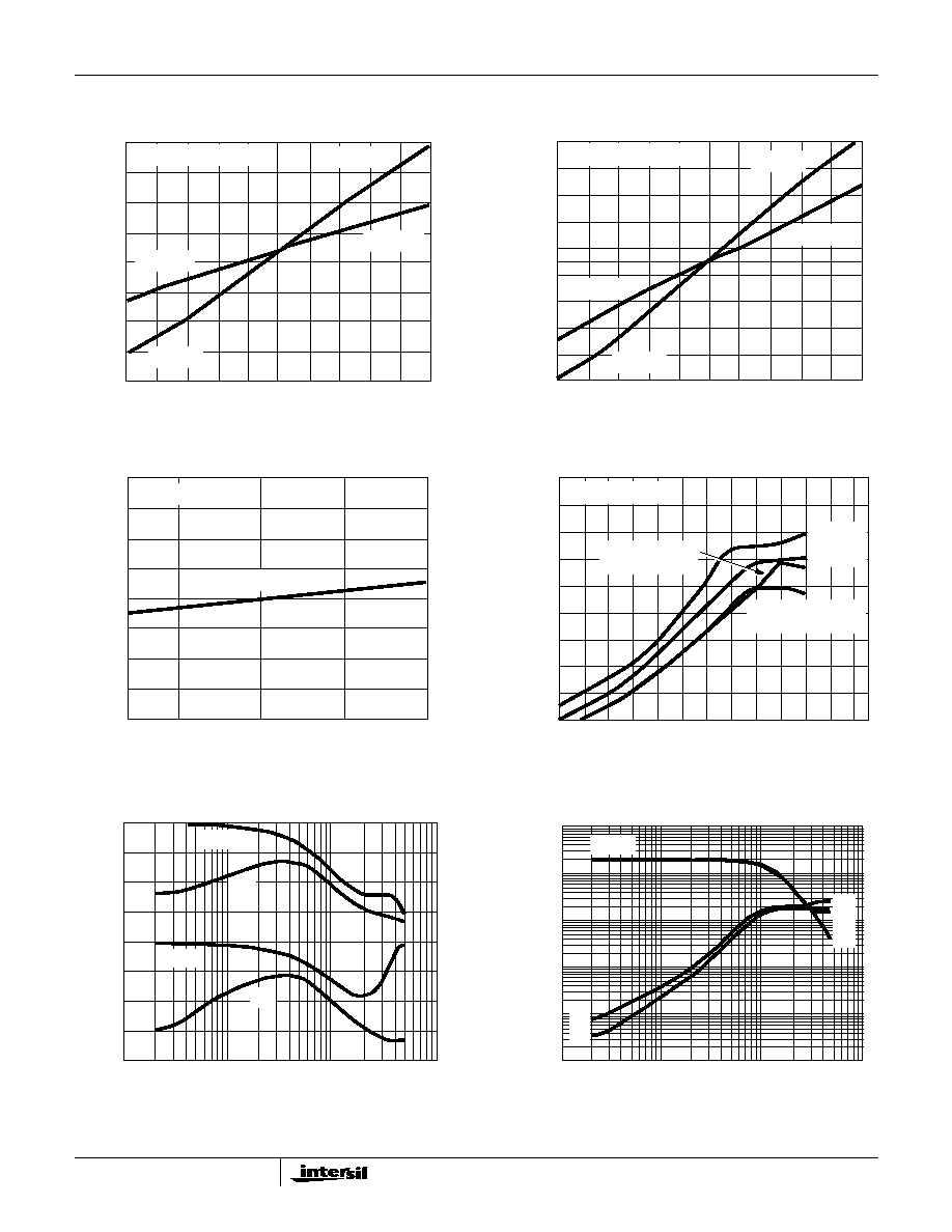
FIGURE 14. GAIN ERROR vs INPUT VOLTAGE
FIGURE 15. GAIN ERROR vs INPUT VOLTAGE
FIGURE 16. GAIN ERROR vs TEMPERATURE
FIGURE 17. V
IN
- V
OUT
vs I
OUT
FIGURE 18. Y - PARAMETERS PHASE vs FREQUENCY
FIGURE 19. Y - PARAMETER MAGNITUDE vs FREQUENCY
Typical Performance Curves
(Continued)
INPUT VOLTAGE (V)
0
+2
+4
+6
+8
+10
-4
-8
-10
OUTPUT INPUT V
OS
(mV)
-80
-40
0
40
80
-6
-2
V
S
=
±
15V, T
A
= 25
o
C
R
L
= 10k
R
L
= 1k
60
20
-20
-60
R
L
= 10k
R
L
= 1k
INPUT VOLTAGE (V)
0
+2
+4
+6
+8
+10
-4
-8
-10
OUTPUT INPUT V
OS
(mV)
-900
-500
0
300
900
-6
-2
V
S
=
±
15V, T
A
= 25
o
C
R
L
= 50
R
L
= 100
R
L
= 100
R
L
= 50
500
100
-100
-700
-300
700
R
L
= 1k
V
S
=
±
15V, V
O
=
±
10V
160
140
120
100
80
-55
25
125
TEMPERATURE (
o
C)
60
40
20
75
-25
OUTPUT INPUT V
OS
(mV)
800
700
600
500
200
0
10
80
90 100
I
OUT
(mA)
V
OUT
= -10
V
IN
- V
OUT
(mV)
20
30
40
50
60
70
V
OUT
= +10
V
OUT
= 0 SINKING
CURRENT
V
OUT
= 0 SOURCING
CURRENT
V
S
=
±
15, T
A
= 25
o
C
400
300
100
110 120
10
6
180
135
90
45
0
-45
-90
-135
-180
PHASE ANGLE (DEGREES)
FREQUENCY (Hz)
Y
12
10
7
10
8
10
9
Y
21
Y
11
Y
22
MA
GNITUDE (S)
1
10
-1
10
-2
10
-3
10
-4
10
-5
10
6
Y
21
, Y
22
Y
11
Y
11
Y
12
10
8
10
7
FREQUENCY (Hz)
10
9
Y
12
Y
22
Y
21
HA-5033
8
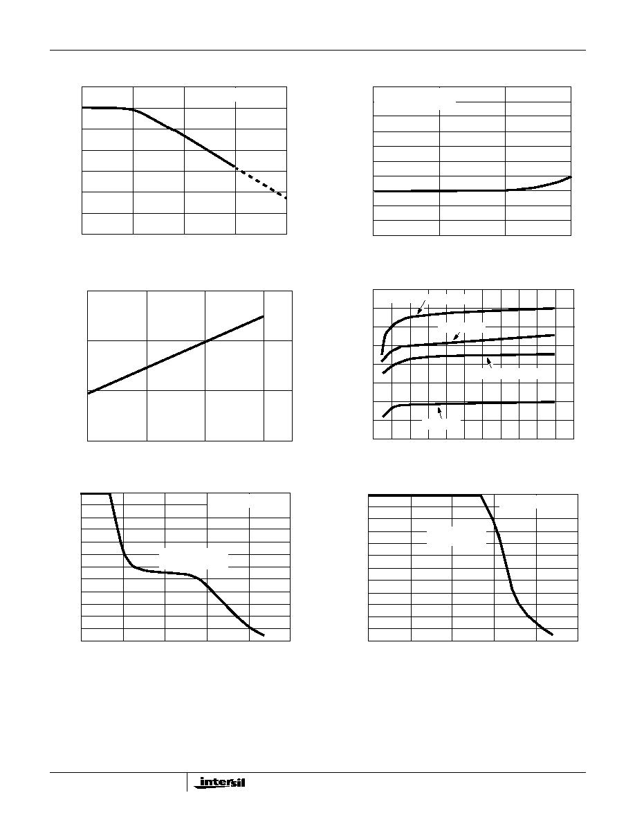
FIGURE 20. POWER SUPPLY REJECTION RATIO vs FREQUENCY
FIGURE 21. TOTAL HARMONIC DISTORTION vs FREQUENCY
FIGURE 22. TOTAL HARMONIC DISTORTION vs INPUT VOLTAGE
FIGURE 23. OUTPUT VOLTAGE SWING vs LOAD RESISTANCE
FIGURE 24. OUTPUT SWING vs FREQUENCY (NOTE)
FIGURE 25. OUTPUT SWING vs FREQUENCY (NOTE)
NOTE:
This curve was obtained by noting the output voltage necessary to produce an observable distortion for a given frequency. If higher distortion is
acceptable, then a higher output voltage for a given frequency can be obtained. However, operating the HA-5033 with increased distortion (to the
right of curve shown), will also be accompanied by an increase in supply current. The resulting increase in chip temperature must be considered
and heat sinking will be necessary to prevent thermal runaway. This characteristic is the result of the output transistor operation. If the signal amplitude
or signal frequency or both are increased beyond the curve shown, the NPN, PNP output transistors will approach a condition of being simultaneously on.
Under this condition, thermal runaway can occur.
Typical Performance Curves
(Continued)
FREQUENCY (Hz)
1K
10K
100K
1M
10M
10
20
30
40
50
60
70
PO
WER SUPPL
Y REJECTION RA
TIO (dB)
V
S
=
±
12V, T
A
= 25
o
C
V
S
=
±
12V, R
L
= 100
V
IN
= 1V
RMS
FREQUENCY (Hz)
100K
10K
1K
100
0.01
0.02
0.03
0.04
0.05
0.06
0.07
0.08
0.09
0.10
T
O
T
AL HARMONIC DIST
OR
TION (%)
INPUT VOLTAGE (RMS)
0
1
2
3
0.01
0.1
1.0
T
O
T
AL HARMONIC DIST
OR
TION (%)
±
V =
±
12V, R
L
= 100
V
S
=
±
12V
R
L
= 100
f = 100kHz
28
24
20
16
12
0
300
600
LOAD RESISTANCE (
)
PEAK T
O
PEAK OUTPUT V
O
L
T
A
GE (V)
8
4
500
400
100 200
700 800 900 1K
T
A
= 25
o
C
V
S
=
±
15V
V
S
=
±
12V
V
S
=
±
10V
V
S
=
±
5V
FREQUENCY (Hz)
10K
100K
1M
10M
0.5
3.5
4.0
4.5
5.0
5.5
6.0
OUTPUT V
O
L
T
A
GE (V
RMS
)
100M
1G
3.0
2.5
2.0
1.5
1.0
0
V
S
=
±
15V, R
L
= 100
NO HEAT SINK IN
FREE AIR
FREQUENCY (Hz)
10K
100K
1M
10M
0.5
3.5
4.0
4.5
5.0
5.5
6.0
OUTPUT V
O
L
T
A
GE (V
RMS
)
V
S
=
±
15V, R
L
= 1k
100M
1G
NO HEAT SINK
IN FREE AIR
3.0
2.5
2.0
1.5
1.0
0
HA-5033
9
All Intersil semiconductor products are manufactured, assembled and tested under ISO9000 quality systems certification.
Intersil semiconductor products are sold by description only. Intersil Corporation reserves the right to make changes in circuit design and/or specifications at any time with-
out notice. Accordingly, the reader is cautioned to verify that data sheets are current before placing orders. Information furnished by Intersil is believed to be accurate and
reliable. However, no responsibility is assumed by Intersil or its subsidiaries for its use; nor for any infringements of patents or other rights of third parties which may result
from its use. No license is granted by implication or otherwise under any patent or patent rights of Intersil or its subsidiaries.
For information regarding Intersil Corporation and its products, see web site http://www.intersil.com
Die Characteristics
DIE DIMENSIONS:
51 mils x 67 mils x 19 mils
1300
µ
m x 1700
µ
m x 483
µ
m
METALLIZATION:
Type: Al, 1% Cu
Thickness: 16k
≈
±
2k
≈
PASSIVATION:
Type: Nitride (Si
3
N
4
) over Silox (SiO
2
, 5% Phos.)
Silox Thickness: 12k
≈
±
2k
≈
Nitride Thickness: 3.5k
≈
±
1.5k
≈
SUBSTRATE POTENTIAL (Powered Up):
Unbiased
TRANSISTOR COUNT:
20
PROCESS:
Bipolar Dielectric Isolation
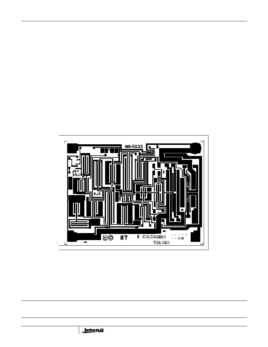
Metallization Mask Layout
HA-5033
V+
OUT
V-
IN
HA-5033