1
July 1997
HA-2529/883
Uncompensated, High Slew Rate
High Output Current, Operational Amplifier
Features
∑ This Circuit is Processed in Accordance to MIL-STD-883
and is Fully Conformant Under the Provisions of Para-
graph 1.2.1.
∑ High Slew Rate . . . . . . . . . . . . . . . . . . . . . 135V/
µ
s (Min)
150V/
µ
s (Typ)
∑ High Output Current . . . . . . . . . . . . . . . . .
±
30mA (Min)
∑ High Gain-Bandwidth Product . . . . . . . . . 15MHz (Min)
20MHz(Typ)
∑ Wide Power Bandwidth . . . . . . . . . . . . . . . 2.1MHz (Min)
∑ High Input Impedance . . . . . . . . . . . . . . . . . 50M
(Min)
130M
(Typ)
∑ Low Offset Current . . . . . . . . . . . . . . . . . . . 25nA (Max)
5nA (Typ)
∑ Fast Settling (10V Step to 0.1%) . . . . . . . . . . . 200ns (Typ)
∑ Low Quiescent Supply Current . . . . . . . . . . 6mA (Max)
Applications
∑ Data Acquisition Systems
∑ RF Amplifiers
∑ Video Amplifiers
∑ Signal Generators
∑ Pulse Amplification
Description
The HA-2529/883 is a monolithic operational amplifier which
typifies excellence of design. With a design based on years
of experience coupled with the reliable dielectric isolation
process, these amplifiers provide an outstanding combina-
tion of DC and AC parameters at closed loop gains of 3 or
greater without external compensation.
The HA-2529/883 offers 135V/
µ
s (min) slew rate and fast
settling time (200ns typ), while consuming a mere 6mA
(max) quiescent supply current, making these amplifiers
ideal components for video circuitry and data acquisition
designs. With 15MHz minimum gain-bandwidth product
combined with 7.5kV/V minimum open loop gain, the
HA-2529/883 is an ideal component for demanding signal
conditioning designs. These devices provide
±
30mA (min)
output current drive with an output voltage swing of
±
10V
(min), making then suited for pulse amplifier and RF ampli-
fier components. HA-2529/883 will upgrade a system pres-
ently using the HA-2520/22/883 or EHA-2520/22/883 in
regards to output current, slew rate, offset voltage drift, and
offset current drift. To insure compliance with slew rate and
transient response specifications, all devices are 100% tested
for AC performance characteristics over full temperature.
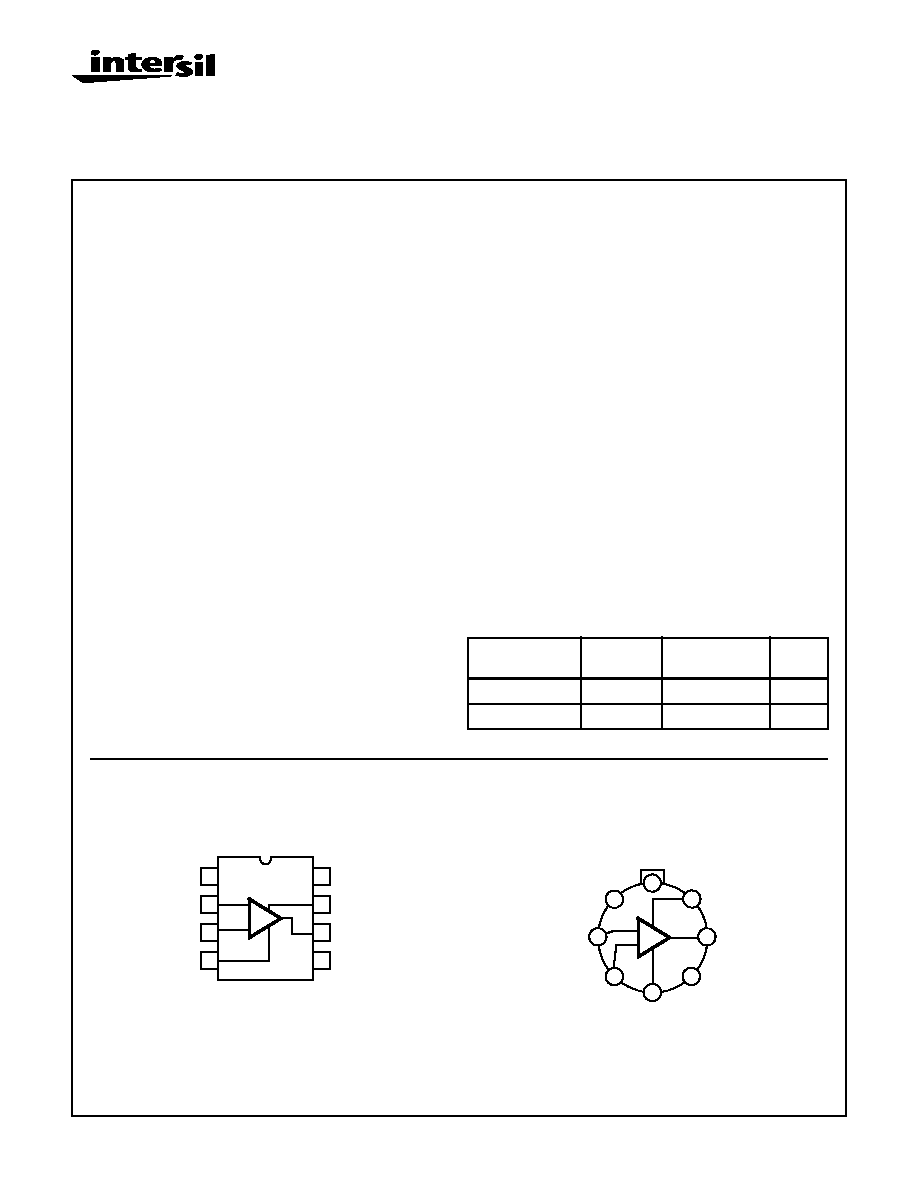
Pinouts
Ordering Information
PART NUMBER
TEMP.
RANGE (
o
C)
PACKAGE
PKG.
NO.
HA2-2529/883
-55 to 125
8 Pin Metal Can
T8.C
HA7-2529/883
-55 to 125
8 Ld CERDIP
F8.3A
HA-2529/883
(CERDIP)
TOP VIEW
HA-2529/883
(METAL CAN)
TOP VIEW
1
2
3
4
8
7
6
5
COMP
V+
OUT
BAL
BAL
-IN
+IN
V-
+
-
2
4
6
1
3
7
5
8
COMP
OUT
-IN
V-
BAL
+IN
V+
BAL
+
-
Spec Number
511025-883
File Number
3736.1
CAUTION: These devices are sensitive to electrostatic discharge; follow proper IC Handling Procedures.
1-888-INTERSIL or 321-724-7143 | Copyright © Intersil Corporation 1999

2
Absolute Maximum Ratings
T
A
= 25
o
C
Thermal Information
Voltage Between V+ and V- Terminals . . . . . . . . . . . . . . . . . . . . 40V
Differential Input Voltage. . . . . . . . . . . . . . . . . . . . . . . . . . . . . . . 15V
Voltage at Either Input Terminal . . . . . . . . . . . . . . . . . . . . . . V+ to V-
Peak Output Current . . . . . . . . . . . . . . . . . . . . . . . . . . . . . . . . 50mA
ESD Rating. . . . . . . . . . . . . . . . . . . . . . . . . . . . . . . . . . . . . . <2000V
Operating Conditions
Temperature Range . . . . . . . . . . . . . . . . . . . . . . . . . -55
o
C to 125
o
C
Supply Voltage
. . . . . . . . . . . . . . . . . . . . . . . . . . . . . . . . . . . . . . . . . ±
15V
V
INCM
1/2 (V+ - V-)
R
L
500
Thermal Resistance (Typical, Note 1)
JA
JC
CERDIP Package . . . . . . . . . . . . . . . .
115
o
C/W
28
o
C/W
Metal Can Package . . . . . . . . . . . . . . .
160
o
C/W
75
o
C/W
Package Power Dissipation Limit at 75
o
C for T
J
175
o
C
CERDIP Package . . . . . . . . . . . . . . . . . . . . . . . . . . . . . . . 870mW
Metal Can Package . . . . . . . . . . . . . . . . . . . . . . . . . . . . . . 625mW
Package Power Dissipation Derating Factor Above 75
o
C
CERDIP Package . . . . . . . . . . . . . . . . . . . . . . . . . . . . . 8.7mW/
o
C
Metal Can Package . . . . . . . . . . . . . . . . . . . . . . . . . . . . 6.3mW/
o
C
Maximum Junction Temperature . . . . . . . . . . . . . . . . . . . . . . . 175
o
C
Maximum Storage Temperature Range . . . . . . . . . .-65
o
C to 150
o
C
Maximum Lead Temperature (Soldering 10s) . . . . . . . . . . . . . 300
o
C
CAUTION: Stresses above those listed in "Absolute Maximum Ratings" may cause permanent damage to the device. This is a stress only rating and operation
of the device at these or any other conditions above those indicated in the operational sections of this specification is not implied.
NOTE:
1.
JA
is measured with the component mounted on an evaluation PC board in free air.
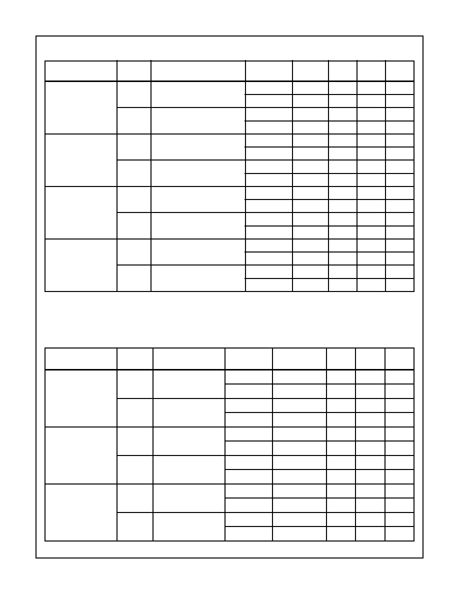
TABLE 1. DC ELECTRICAL PERFORMANCE CHARACTERISTICS
Device Tested at: V
SUPPLY
=
±
15V, R
SOURCE
= 100
, R
LOAD
= 500k
, V
OUT
= 0V, Unless Otherwise Specified.
PARAMETER
SYMBOL
CONDITIONS
GROUP A
SUBGROUPS
TEMP.
(
o
C)
MIN
MAX
UNITS
Input Offset Voltage
V
IO
V
CM
= 0V
1
25
-5
5
mV
2, 3
125, -55
-8
8
mV
Input Bias Current
+I
B
V
CM
= 0V, +R
S
= 100k
,
-R
S
= 100
1
25
-200
200
nA
2, 3
125, -55
-400
400
nA
-I
B
V
CM
= 0V, +R
S
= 100
,
-R
S
= 100k
1
25
-200
200
nA
2, 3
125, -55
-400
400
nA
Input Offset
Current
I
IO
V
CM
= 0V, +R
S
= 100k
,
-R
S
= 100k
1
25
-25
25
nA
2, 3
125, -55
-50
50
nA
Common Mode Range
+CMR
V+ = 5V, V- = -25V
1
25
+10
-
V
2, 3
125, -55
+10
-
V
-CMR
V+ = 25V, V- = -5V
1
25
-
-10
V
2, 3
125, -55
-
-10
V
Large Signal Voltage
Gain
+A
VOL
V
OUT
= 0V and +10V, R
L
= 2k
4
25
10
-
kV/V
5, 6
125, -55
7.5
-
kV/V
-A
VOL
V
OUT
= 0V and -10V, R
L
= 2k
4
25
10
-
kV/V
5, 6
125, -55
7.5
-
kV/V
Common Mode
Rejection Ratio
+CMRR
V
CM
= +10V, V+ = +5V,
V- = -25V,
V
OUT
= -10V
1
25
83
-
dB
2, 3
125, -55
80
-
dB
-CMRR
V
CM
= -10V, V+ = +25V,
V- = -5V, V
OUT
= +10V
1
25
83
-
dB
2, 3
125, -55
80
-
dB
Output Voltage Swing
+V
OUT
R
L
= 2k
4
25
10
-
V
5, 6
125, -55
10
-
V
-V
OUT
R
L
= 2k
4
25
-
-10
V
5, 6
125, -55
-
-10
V
HA-2529/883
Spec Number
511025-883
3
Output Current
+I
OUT
V
OUT
= -10V
4
25
30
-
mA
5, 6
125, -55
20
-
mA
-I
OUT
V
OUT
= +10V
4
25
-
-30
mA
5, 6
125, -55
-
-20
mA
Quiescent Power Supply
Current
+I
CC
V
OUT
= 0V, I
OUT
= 0mA
1
25
-
6
mA
2, 3
125, -55
-
7
mA
-I
CC
V
OUT
= 0V, I
OUT
= 0mA
1
25
-6
-
mA
2, 3
125, -55
-7
-
mA
Power Supply
Rejection Ratio
+PSRR
V
SUP
= 10V, V+ = +20V,
V- = -15V, V+ = +10V, V- = -15V
1
25
80
-
dB
2, 3
125, -55
80
-
dB
-PSRR
V
SUP
= 10V, V+ = +15V,
V- = -20V, V+ = +15V, V- = -10V
1
25
80
-
dB
2, 3
125, -55
80
-
dB
Offset Voltage
Adjustment
+V
IO
Adj
Note 2
1
25
V
IO
-1
-
mV
2, 3
125, -55
V
IO
-1
-
mV
-V
IO
Adj
Note 2
1
25
V
IO
+1
-
mV
2, 3
125, -55
V
IO
+1
-
mV
NOTE:
2. Offset adjustment range is [V
IO
(Measured)
±
1mV] minimum referred to output. This test is for functionality only to assure adjustment
through 0V.
TABLE 2. AC ELECTRICAL PERFORMANCE CHARACTERISTICS
Device Tested at: V
SUPPLY
=
±
15V, R
SOURCE
= 50
, R
LOAD
= 2k
, C
LOAD
= 50pF, A
VCL
= +3V/V, Unless Otherwise Specified.
PARAMETERS
SYMBOL
CONDITIONS
GROUP A
SUBGROUPS
TEMP. (
o
C)
MIN
MAX
UNITS
Slew Rate
+SR
V
OUT
= -5V to +5V
25%
+SR
75%
7
25
135
-
V/
µ
s
8A, 8B
125, -55
125
-
V/
µ
s
-SR
V
OUT
= +5V to -5V
75%
-SR
25%
7
25
135
-
V/
µ
s
8A, 8B
125, -55
125
-
V/
µ
s
Rise and Fall Time
t
r
V
OUT
= 0 to +200mV
10%
t
r
90%
7
25
-
45
ns
8A, 8B
125, -55
-
50
ns
t
f
V
OUT
= 0 to -200mV
10%
t
f
90%
7
25
-
45
ns
8A, 8B
125, -55
-
50
ns
Overshoot
+OS
V
OUT
= 0 to +200mV
7
25
-
40
%
8A, 8B
125, -55
-
40
%
-OS
V
OUT
= 0 to -200mV
7
25
-
40
%
8A, 8B
125, -55
-
40
%
TABLE 1. DC ELECTRICAL PERFORMANCE CHARACTERISTICS (Continued)
Device Tested at: V
SUPPLY
=
±
15V, R
SOURCE
= 100
, R
LOAD
= 500k
, V
OUT
= 0V, Unless Otherwise Specified.
PARAMETER
SYMBOL
CONDITIONS
GROUP A
SUBGROUPS
TEMP.
(
o
C)
MIN
MAX
UNITS
HA-2529/883
Spec Number
511025-883
4
Spec Number
511025-883
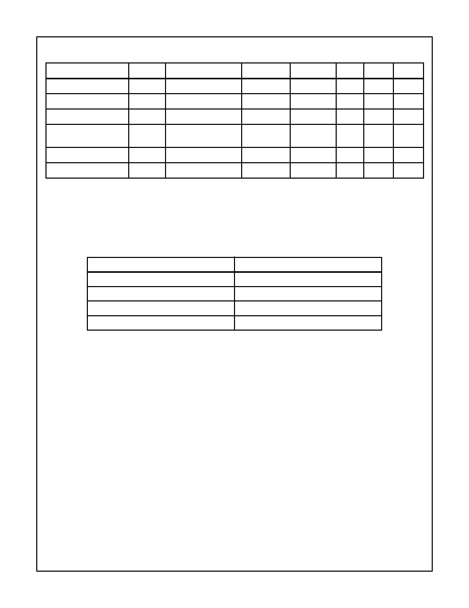
TABLE 3. ELECTRICAL PERFORMANCE CHARACTERISTICS
Device Characterized at: V
SUPPLY
=
±
15V, R
LOAD
= 2k
, C
LOAD
= 50pF, C
COMP
= 0pF, Unless Otherwise Specified.
PARAMETERS
SYMBOL
CONDITIONS
NOTES
TEMP. (
o
C)
MIN
MAX
UNITS
Differential Input Resistance
R
IN
V
CM
= 0V
3
25
50
-
M
Gain Power Bandwidth
GBWP
V
O
= 200mV, f
O
10kHz
3
25
15
-
MHz
Full Power Bandwidth
FPBW
V
PEAK
= 10V
3, 4
25
2.1
-
MHz
Minimum Closed Loop
Stable Gain
CLSG
R
L
= 2k
, C
L
= 50pF
3
-55 to 125
±
3
-
V/V
Output Resistance
R
OUT
Open Loop
3
25
-
60
Power Consumption
PC
V
OUT
= 0V, I
OUT
= 0mA
3, 5
-55 to 125
-
210
mW
NOTES:
3. Parameters listed in Table 3 are controlled via design or process parameters and are not directly tested at final production. These param-
eters are lab characterized upon initial design release, or upon design changes. These parameters are guaranteed by characterization
based upon data from multiple production runs which reflect lot to lot and within lot variation.
4. Full Power Bandwidth guarantee based on Slew Rate measurement using FPBW = Slew Rate/(2
V
PEAK
).
5. Quiescent Power Consumption based upon Quiescent Supply Current test maximum. (No load on outputs.)
TABLE 4. ELECTRICAL TEST REQUIREMENTS
MIL-STD-883 TEST REQUIREMENTS
SUBGROUPS (SEE TABLES 1 AND 2)
Interim Electrical Parameters (Pre Burn-In)
1
Final Electrical Test Parameters
1 (Note 6), 2, 3, 4, 5, 6, 7, 8A, 8B
Group A Test Requirements
1, 2, 3, 4, 5, 6, 7, 8A, 8B
Groups C and D Endpoints
1
NOTE:
6. PDA applies to Subgroup 1 only.
HA-2529/883
5
Spec Number
511025-883
Die Characteristics
DIE DIMENSIONS:
67 mils x 57 mils x 19 mils
1700
µ
m x 1440
µ
m x 483
µ
m
METALLIZATION:
Type: Al, 1% Cu
Thickness: 16k
≈
±
2k
≈
GLASSIVATION:
Type: Nitride (Si3N4) over Silox (SiO2, 5% Phos.)
Silox Thickness: 12k≈
±
2k≈
Nitride Thickness: 3.5k≈
±
1.5k≈
WORST CASE CURRENT DENSITY:
0.78 x 10
5
A/cm
2
SUBSTRATE POTENTIAL (Powered Up):
Unbiased
TRANSISTOR COUNT: 40
PROCESS: Bipolar Dielectric Isolation
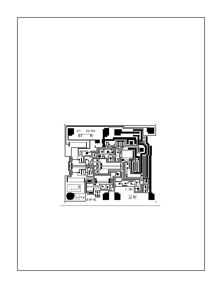
Metallization Mask Layout
HA-2529/883
COMP
V+
OUT
BAL
BAL
-IN
+IN
V-
HA-2529/883
6
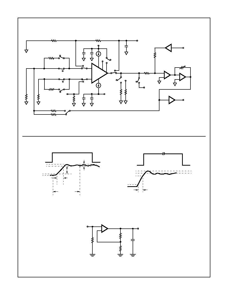
Test Circuit
(Applies to Tables 1 and 2)
Test Circuits and Waveforms
FIGURE 1. SLEW RATE AND SETTLING TIME
NOTE:
Measured on both positive and negative transitions from 0V
to +200mV and 0V to -200mV at the output.
FIGURE 2. TRANSIENT RESPONSE
FIGURE 3. SIMPLIFIED TEST CIRCUIT (APPLIES TO TABLE 2)
100K
1 OPEN
2
S
3A
S
1
1
OPEN 2
S
5A
1
2
100K
1
2
S
3B
S
2
1
OPEN 2
S
6
1
2
0.1
1
0.1
1
V
AC
50
OPEN
V-
667
100
100
5K
50K
2
1
S
4
1.33K
DUT
-
+
V+
S
5B
1
2
S
7
1
2
3
OPEN
2
3
S
8
OPEN 1
10K
2K
50pF
(NOTE)
AC
OUT
NOTE: Includes stray
capacitances
S
9
OPEN
1
2
V2
500K
50K
-1/10
V
1
For loop stability, use min value
capacitor to prevent oscillation
BUFFER
-
+
-
+
-1
x2
E
OUT
ALL RESISTORS =
±
1% (
)
ALL CAPACITORS =
±
10% (
µ
F)
+1.67V
INPUT
+5V
90%
OUTPUT
10%
ERROR BAND
±
10mV FROM
FINAL VALUE
t
SLEW
=
V/
t
-1.67V
V
-5V
RATE
SETTLING
TIME
INPUT
90%
OUTPUT
10%
0mV
RISE TIME
67mV
0V
+200mV
OVERSHOOT
0
-67mV
V
OUT
V
IN
1.33k
50pF
667
50
+
-
HA-2529/883
Spec Number
511025-883
7
Burn-In Circuits
HA7-2529/883 CERDIP
HA2-2529/883 METAL CAN
NOTES:
R
1
= 1M
,
±
5%, 1/4W (Min)
C
1
= C
2
= 0.01
µ
F/Socket (Min) or 0.1
µ
F/Row (Min)
C
3
= 0.01
µ
F/Socket (10%)
D
1
= D
2
= 1N4002 or Equivalent/Board
|(V+) - (V-)| = 30V
V+
C
1
D
1
R
1
D
2
C
2
V-
+
-
1
3
4
8
7
6
5
2
C
3
1
5
8
+
-
V+
C
1
D
1
6
2
7
C
3
3
R
1
4
C
2
D
2
V-
8
HA-2529/883
Spec Number
511025-883
NOTES:
1. Index area: A notch or a pin one identification mark shall be locat-
ed adjacent to pin one and shall be located within the shaded
area shown. The manufacturer's identification shall not be used
as a pin one identification mark.
2. The maximum limits of lead dimensions b and c or M shall be
measured at the centroid of the finished lead surfaces, when
solder dip or tin plate lead finish is applied.
3. Dimensions b1 and c1 apply to lead base metal only. Dimension
M applies to lead plating and finish thickness.
4. Corner leads (1, N, N/2, and N/2+1) may be configured with a
partial lead paddle. For this configuration dimension b3 replaces
dimension b2.
5. This dimension allows for off-center lid, meniscus, and glass
overrun.
6. Dimension Q shall be measured from the seating plane to the
base plane.
7. Measure dimension S1 at all four corners.
8. N is the maximum number of terminal positions.
9. Dimensioning and tolerancing per ANSI Y14.5M - 1982.
10. Controlling dimension: INCH.
bbb
C A - B
S
c
Q
L
A
SEATING
BASE
D
PLANE
PLANE
-D-
-A-
-C-
-B-
D
E
S1
b2
b
A
e
M
c1
b1
(c)
(b)
SECTION A-A
BASE
LEAD FINISH
METAL
e
A/2
A
M
S
S
ccc
C A - B
M
D
S
S
aaa
C A - B
M
D
S
S
e
A
Ceramic Dual-In-Line Frit Seal Packages (CERDIP)
F8.3A
MIL-STD-1835 GDIP1-T8 (D-4, CONFIGURATION A)
8 LEAD CERAMIC DUAL-IN-LINE FRIT SEAL PACKAGE
SYMBOL
INCHES
MILLIMETERS
NOTES
MIN
MAX
MIN
MAX
A
-
0.200
-
5.08
-
b
0.014
0.026
0.36
0.66
2
b1
0.014
0.023
0.36
0.58
3
b2
0.045
0.065
1.14
1.65
-
b3
0.023
0.045
0.58
1.14
4
c
0.008
0.018
0.20
0.46
2
c1
0.008
0.015
0.20
0.38
3
D
-
0.405
-
10.29
5
E
0.220
0.310
5.59
7.87
5
e
0.100 BSC
2.54 BSC
-
eA
0.300 BSC
7.62 BSC
-
eA/2
0.150 BSC
3.81 BSC
-
L
0.125
0.200
3.18
5.08
-
Q
0.015
0.060
0.38
1.52
6
S1
0.005
-
0.13
-
7
90
o
105
o
90
o
105
o
-
aaa
-
0.015
-
0.38
-
bbb
-
0.030
-
0.76
-
ccc
-
0.010
-
0.25
-
M
-
0.0015
-
0.038
2, 3
N
8
8
8
Rev. 0 4/94
9
All Intersil semiconductor products are manufactured, assembled and tested under ISO9000 quality systems certification.
Intersil products are sold by description only. Intersil Corporation reserves the right to make changes in circuit design and/or specifications at any time without
notice. Accordingly, the reader is cautioned to verify that data sheets are current before placing orders. Information furnished by Intersil is believed to be accurate
and reliable. However, no responsibility is assumed by Intersil or its subsidiaries for its use; nor for any infringements of patents or other rights of third parties which
may result from its use. No license is granted by implication or otherwise under any patent or patent rights of Intersil or its subsidiaries.
For information regarding Intersil Corporation and its products, see web site http://www.intersil.com
Sales Office Headquarters
NORTH AMERICA
Intersil Corporation
P. O. Box 883, Mail Stop 53-204
Melbourne, FL 32902
TEL: (321) 724-7000
FAX: (321) 724-7240
EUROPE
Intersil SA
Mercure Center
100, Rue de la Fusee
1130 Brussels, Belgium
TEL: (32) 2.724.2111
FAX: (32) 2.724.22.05
ASIA
Intersil (Taiwan) Ltd.
Taiwan Limited
7F-6, No. 101 Fu Hsing North Road
Taipei, Taiwan
Republic of China
TEL: (886) 2 2716 9310
FAX: (886) 2 2715 3029
HA-2529/883
Spec Number
511025-883
Metal Can Packages (Can)
NOTES:
1. (All leads) ÿb applies between L1 and L2. ÿb1 applies between
L2 and 0.500 from the reference plane. Diameter is uncontrolled
in L1 and beyond 0.500 from the reference plane.
2. Measured from maximum diameter of the product.
3.
is the basic spacing from the centerline of the tab to terminal 1
and
is the basic spacing of each lead or lead position (N -1
places) from
,
looking at the bottom of the package.
4. N is the maximum number of terminal positions.
5. Dimensioning and tolerancing per ANSI Y14.5M - 1982.
6. Controlling dimension: INCH.
ÿb
ÿD2
ÿ
e
k1
k
ÿb1
BASE AND
SEATING PLANE
F
Q
ÿD ÿD1
L1
L2
REFERENCE PLANE
L
A
ÿb2
ÿb1
BASE METAL
LEAD FINISH
SECTION A-A
A
A
N
e
1
C
L
2
1
T8.C
MIL-STD-1835 MACY1-X8 (A1)
8 LEAD METAL CAN PACKAGE
SYMBOL
INCHES
MILLIMETERS
NOTES
MIN
MAX
MIN
MAX
A
0.165
0.185
4.19
4.70
-
ÿb
0.016
0.019
0.41
0.48
1
ÿb1
0.016
0.021
0.41
0.53
1
ÿb2
0.016
0.024
0.41
0.61
-
ÿD
0.335
0.375
8.51
9.40
-
ÿD1
0.305
0.335
7.75
8.51
-
ÿD2
0.110
0.160
2.79
4.06
-
e
0.200 BSC
5.08 BSC
-
e1
0.100 BSC
2.54 BSC
-
F
-
0.040
-
1.02
-
k
0.027
0.034
0.69
0.86
-
k1
0.027
0.045
0.69
1.14
2
L
0.500
0.750
12.70
19.05
1
L1
-
0.050
-
1.27
1
L2
0.250
-
6.35
-
1
Q
0.010
0.045
0.25
1.14
-
45
o
BSC
45
o
BSC
3
45
o
BSC
45
o
BSC
3
N
8
8
4
Rev. 0 5/18/94