 | –≠–ª–µ–∫—Ç—Ä–æ–Ω–Ω—ã–π –∫–æ–º–ø–æ–Ω–µ–Ω—Ç: HA-2557 | –°–∫–∞—á–∞—Ç—å:  PDF PDF  ZIP ZIP |

8-1
Æ
September 1998
HA-2557
130MHz, Four Quadrant,
Current Output Analog Multiplier
CAUTION: These devices are sensitive to electrostatic discharge; follow proper IC Handling Procedures.
1-888-INTERSIL or 321-724-7143
|
Intersil (and design) is a registered trademark of Intersil Americas Inc.
Copyright © Intersil Americas Inc. 2002. All Rights Reserved
File Number
2478.6
Features
∑ Low Multiplication Error . . . . . . . . . . . . . . . . . . . . . 1.5%
∑ Input Bias Currents . . . . . . . . . . . . . . . . . . . . . . . . . . 8
µ
A
∑ Y Input Feedthrough at 5MHz . . . . . . . . . . . . . . . . -50dB
∑ Wide Y Channel Bandwidth . . . . . . . . . . . . . . . 130MHz
∑ Wide X Channel Bandwidth . . . . . . . . . . . . . . . . 75MHz
Applications
∑ Military Avionics
∑ Medical Imaging Displays
∑ Video Mixers
∑ Sonar AGC Processors
∑ Radar Signal Conditioning
∑ Voltage Controlled Amplifier
∑ Vector Generator
Description
The HA-2557 is a monolithic, high speed, four quadrant,
analog multiplier constructed in Harris' Dielectrically Isolated
High Frequency Process. The single-ended current output of
the HA-2557 has a 130MHz signal bandwidth (R
L
= 50
).
High bandwidth and low distortion make this part an ideal
component in video systems.
The suitability for precision video applications is demon-
strated further by low multiplication error (1.5%), low
feedthrough (-50dB), and differential inputs with low bias
currents (8
µ
A). The HA-2557 is also well suited for mixer cir-
cuits as well as AGC applications for sonar, radar, and med-
ical imaging equipment.
The current output of the HA-2557 allows it to achieve higher
bandwidths than voltage output multipliers. Full scale output
current is trimmed to 1.6mA. An internal 2500
feedback
resistor is also provided to accurately convert the current, if
desired, to a full scale output voltage of
±
4V. The HA-2557 is
not limited to multiplication applications only; frequency dou-
bling and power detection are also possible.
For MIL-STD-883 compliant product consult the HA-2557/883
datasheet.
Part Number Information
PART NUMBER
TEMP.
RANGE (
o
C)
PACKAGE
PKG.
NO.
HA3-2557-9
-40 to 85
16 Ld PDIP
E16.3
HA9P2557-9
-40 to 85
16 Ld SOIC
M16.3
Pinout
HA-2557
(PDIP, SOIC)
TOP VIEW
Schematic
14
15
16
9
13
12
11
10
1
2
3
4
5
7
6
8
V
REF
V
YIO
B
V
YIO
A
V
XIO
A
REF
NC
V
XIO
B
NC
X
I
OUT
R
Z
GND
V
Y
+
V
Y
-
V-
V+
V
X
-
V
X
+
X
Y
V
YIO
B
V
Y
+
V+
V
BIAS
R
Z
I
OUT
V
XIO
A
REF
GND
V
BIAS
V
X
+
Y
Y
-
V
X
-
V
XIO
B
V
YIO
A
V-
+
-
OBS
OLE
TE P
ROD
UCT
REC
OMM
END
ED R
EPL
ACE
MEN
T
HA-2
556
cont
act o
ur Te
chni
cal S
uppo
rt Ce
nter
at
1-88
8-INT
ERS
IL or
www
.inte
rsil.c
om/t
sc

8-2
Absolute Maximum Ratings
Thermal Information
Voltage Between V+ and V- Terminals . . . . . . . . . . . . . . . . . . . 35V
Differential Input Voltage . . . . . . . . . . . . . . . . . . . . . . . . . . . . . . . 6V
Output Current . . . . . . . . . . . . . . . . . . . . . . . . . . . . . . . . . . . . . . 3mA
Operating Conditions
Temperature Range . . . . . . . . . . . . . . . . . . . . . . . . . -40
o
C to 85
o
C
Thermal Resistance (Typical, Note 1)
JA
(
o
C/W)
PDIP Package . . . . . . . . . . . . . . . . . . . . . . . . . . . . .
77
SOIC Package. . . . . . . . . . . . . . . . . . . . . . . . . . . . .
90
Maximum Junction Temperature (Die) . . . . . . . . . . . . . . . . . . . 175
o
C
Maximum Junction Temperature (Plastic Package) . . . . . . . . 150
o
C
Maximum Storage Temperature Range . . . . . . . . . -65
o
C to 150
o
C
Maximum Lead Temperature (Soldering 10s). . . . . . . . . . . . 300
o
C
(SOIC - Lead Tips Only)
CAUTION: Stresses above those listed in "Absolute Maximum Ratings" may cause permanent damage to the device. This is a stress only rating and operation
of the device at these or any other conditions above those indicated in the operational sections of this specification is not implied.
NOTE:
1.
JA
is measured with the component mounted on an evaluation PC board in free air.
Electrical Specifications
V
SUPPLY
=
±
15V, Unless Otherwise Specified
PARAMETER
TEST CONDITIONS
TEMP.
(
o
C)
HA-2557-9
UNITS
MIN
TYP
MAX
MULTIPLIER PERFORMANCE
Transfer Function
Multiplication Error (Note 2)
25
-
1.5
3
%FS
Full
-
3.0
6
%FS
Multiplication Error Drift
Full
-
0.003
-
%/
o
C
Scale Factor
25
-
10
-
kV
Linearity Error
V
X
, V
Y
=
±
4V, Full Scale = 4V
25
-
0.1
0.25
%
V
X
, V
Y
=
±
3V, Full Scale = 3V
25
-
0.05
-
%
AC CHARACTERISTICS
Small Signal Bandwidth (-3dB)
(R
L
= 50
)
V
Y
= 200mV
P-P
, V
X
= 4V
25
-
130
-
MHz
V
X
= 200mV
P-P
, V
Y
= 4V
25
-
75
-
MHz
Rise Time
V
OUT
= -80mV to +80mV, R
L
= 50
25
-
7
-
ns
Propagation Delay
R
L
= 50
25
-
3
-
ns
Feedthrough (Note 4)
f = 5MHz
25
-
-50
-
dB
THD+N
f = 10kHz, V
Y
= 1V
RMS
, V
X
= 4V
25
-
0.03
-
%
SIGNAL INPUT V
X
, V
Y
Input Offset Voltage
25
-
4
15
mV
Full
-
8
25
mV
Average Offset Voltage Drift
Full
-
35
-
µ
V/
o
C
Input Bias Current
25
-
8
15
µ
A
Full
-
12
25
µ
A
Input Offset Current
25
-
0.5
2
µ
A
Full
-
1.0
3
µ
A
Differential Input Resistance
25
-
1
-
M
Differential Input Range
25
±
4
-
-
V
CMRR
Note 3
Full
65
78
-
dB
Voltage Noise (Pin 10 = GND
V
X
= V
Y
= GND)
f = 1kHz
25
-
150
-
nV/
Hz
f = 100kHz
25
-
40
-
nV/
Hz
OUTPUT CHARACTERISTICS
Output Offset Current
25
-
2.4
10
µ
A
Full
-
5.6
15
µ
A
Full Scale Output Compliance
Voltage
Full
±
4
-
-
V
Full Scale Output Current
25
-
±
1.6
-
mA
I
OUT
V
X+
V
X-
≠
(
)
V
Y+
V
Y-
≠
(
)
◊
10kV
--------------------------------------------------------------------
=
HA-2557
8-3
Test Circuit and Waveform
Application Information
Operation at Reduced Supply Voltages
The HA-2557 will operate over a range of supply voltages,
±
5V to
±
15V. Use of supply voltages below
±
12V will reduce
input and output voltage ranges. See "Typical Performance
Curves" for more information. The
±
5V range is particularly
useful in video applications. At
±
5V the input voltage range is
reduced to
±
1.4V limiting the fullscale output current.
Another current output option is the HA-2556 voltage output
multiplier configured for current output with an output sens-
ing resistor (Refer to the HA-2556 data sheet).
Offset Adjustment
The channel offset voltage may be nulled by using a 20K poten-
tiometer between the V
YIO
or V
XIO
adjust pin A and B and con-
necting the wiper to V-. Reducing the channel offset voltage will
reduce AC feedthrough and improve the multiplication error.
Theory of Operation
The HA-2557 creates an output current that is the product of
the X and Y input voltages divided by a constant scale factor of
10kV
. The resulting output has the correct polarity in each of
the four quadrants defined by the combinations of positive and
negative X and Y inputs. This results in the following equation,
where X and Y are high impedance differential inputs:
To accomplish this the differential input voltages are first con-
verted into differential currents by the X and Y input transcon-
ductance stages. The currents are then scaled by a constant
reference and combined in the multiplier core. The multiplier
core is a basic Gilbert Cell that produces a differential output
current proportional to the product of X and Y input signal cur-
rents. This current is converted into the output for the HA-2557.
The purpose of the reference circuit is to provide a stable cur-
rent, used in setting the scale factor. This is achieved with a
bandgap reference circuit to produce a temperature stable
voltage of 1.2V which is forced across a NiCr resistor. Slight
adjustments to scale factor may be possible by overriding the
Output Resistance
±
10V
25
1.0
1.5
-
M
Output Capacitance
25
-
6.5
-
pF
Internal Resistor (R
Z
)
25
2425
2500
2575
Full
2375
2500
2625
POWER SUPPLY
+PSRR
V
S
=
±
12V to
±
17V
Full
65
80
-
dB
-PSRR
V
S
=
±
12V to
±
17V
Full
45
55
-
dB
Supply Current
Full
-
13
17
mA
NOTES:
2. Error is percent of full scale, 1% = 16
µ
A.
3. V
XCM
=
±
10V, V
YCM
= +9V, -10V.
4. Relative to full scale output.
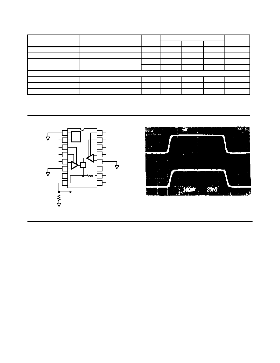
FIGURE 1. AC AND TRANSIENT RESPONSE TEST CIRCUIT
V
Y
TRANSIENT RESPONSE
Electrical Specifications
V
SUPPLY
=
±
15V, Unless Otherwise Specified (Continued)
PARAMETER
TEST CONDITIONS
TEMP.
(
o
C)
HA-2557-9
UNITS
MIN
TYP
MAX
14
15
16
9
13
12
11
10
1
2
3
4
5
7
6
8
+15V
V
OUT
NC
NC
NC
-15V
50
NC
V
Y
+
V
X
+
REF
NC
NC
NC
NC
X
Y
X
Vertical Scale: Top 5V/Div. Bottom: 100mV/Div.
Horizontal Scale: 20ns/Div.
I
OUT
X x Y
10kV
-------------------
=
HA-2557

8-4
internal reference with the V
REF
pin. The scale factor is used
to maintain the output of the multiplier within the normal oper-
ating range of
±
1.6mA when full scale inputs are applied.
Typical Applications
Communication Applications
The multiplier function of the HA-2557 has applications in
AM Signal Generation, Synchronous AM Detection and
Phase Detection. These circuit configurations are shown in
Figure 2, Figure 3 and Figure 4. By feeding a signal into both
X and Y inputs a Square function results that is useful as a
Frequency Doubler as shown in Figure 5. The HA-2557 is
particularly useful in applications that require the interaction
of high speed signals. Both inputs X and Y have similar wide
bandwidth and input characteristics. This is unlike earlier
products where one input was dedicated to a slow moving
control function as is required for Automatic Gain Control.
The HA-2557 is versatile enough for both.
Although the X and Y inputs have similar AC characteristics,
they are not the same. The designer should consider input
parameters such as small signal bandwidth and AC
feedthrough to get the most performance from the HA-2557.
The Y channel is the faster of the two inputs with a small sig-
nal bandwidth of typically 130MHz verses 75MHz for the X
channel. Therefore in AM Signal Generation, the best perfor-
mance will be obtained with the Carrier applied to the Y
channel and the modulation signal (lower frequency) applied
to the X channel.
1/10kV
X
Y
V
X
+
V
X
-
V
Y
+
V
Y
-
X
I
OUT
ACOS(
)
CCOS(
C
)
CARRIER
AUDIO
IOUT
AC
20kV
-----------------
Cos
C
A
≠
(
)
Cos
C
A
+
(
)
+
(
)
=
R
Z
+
-
+
-
FIGURE 2. AM SIGNAL GENERATION
1/10kV
X
Y
V
X
+
V
X
-
V
Y
+
V
Y
-
AM SIGNAL
CARRIER
LIKE THE FREQUENCY DOUBLER YOU GET
I
OUT
R
Z
+
-
+
-
X
AUDIO CENTERED AT DC AND 2F
C
.
FIGURE 3. SYNCHRONOUS AM DETECTION
1/10kV
X
Y
V
X
+
V
X
-
V
Y
+
V
Y
-
ACOS(
)
ACOS(
+
)
I
OUT
A
2
20kV
-------------------
Cos
( )
Cos 2
+
(
)
+
(
)
=
DC COMPONENT IS PROPORTIONAL TO COS(
)
I
OUT
R
Z
+
-
+
-
X
FIGURE 4. PHASE DETECTION
1/10kV
X
Y
I
OUT
V
X
+
V
X
-
V
Y
+
V
Y
-
ACOS(
)
ACos
(
)
ACos
(
)
◊
(
)
10kV
I
OUT
(
)
=
I
OUT
A
2
20K
-----------
1 Cos 2
(
)
+
(
)
=
R
Z
WHICH EVALUATES TO:
+
-
+
-
X
FIGURE 5. FREQUENCY DOUBLER
HA-2557

8-5
Automatic Gain Control
Figure 6 shows the HA-2557 configured in an Automatic Gain
Control or AGC application. The HA-2842 serves as an output I
to V converter using R
Z
which is trimmed to provide an
accurate 4V Fullscale conversion. Refer to Voltage Output
Conversion for more details about this function. The HA-5127
low noise amplifier provides the gain control signal to the X
input. This control signal sets the peak output voltage of the
multiplier to match the preset reference level. The feedback
network around the HA-5127 provides a response time
adjustment. High frequency changes in the peak are rejected
as noise or the desired signal to be transmitted. These signals
do not indicate a change in the average peak value and
therefore no gain adjustment is needed. Lower frequency
changes in the peak value are given a gain of -1 for feedback to
the control input. At DC the circuit is an integrator automatically
compensating for offset and other constant error terms.
This multiplier has the advantage over other AGC circuits, in
that the signal bandwidth is not affected by the control signal
gain adjustment.
Voltage Output Conversion
The HA-2842 is an excellent choice to perform the output
current to voltage conversion as shown in Figure 7. The
combination of 400V/
µ
s slew rate and 80MHz Gain Band-
width product will maintain signal dynamics while providing a
full scale
±
4V output. The HA-2842 also provides a hefty out-
put drive capability of 100mA.
This voltage feedback amplifier takes advantage of the inter-
nal R
Z
resistor, trimmed to provide an accurate 4V fullscale
conversion. The parasitic capacitance at the negative input
of the HA-2842 must be compensated with a 3pF capacitor
from pin 2 to pin 6. This compensation will also insure that
the amp will see a noise gain of 2 at its crossover frequency,
the minimum required for stability with this device. The full
power bandwidth curve and large signal pulse response for
this circuit are shown in Figure 11 and Figure 12 respec-
tively. The fast slew rate of the HA-2842 results in a minimal
reduction of bandwidth for large signals.
Another choice for an I to V converter that takes better
advantage of the wide bandwidth of the HA-2557, is to use
the HA5023 Dual 100MHz current feedback amp. The opti-
mum bandwidth of a current feedback amp is obtained with a
fixed feedback resistor. Therefore scaling the I to V conver-
sion to a convenient value requires two stages. Fortunately
the HA5023 provides two wideband amplifiers in a single 8
pin Mini-DIP or SOIC package, while their current feedback
architecture provides signal gain with minimal reduction in
bandwidth. This circuit configuration is shown in Figure 8.
The optimum bandwidth is achieved in stage 1 with a 909
feedback resistor. This voltage is then gained up by the sec-
ond stage to provide a
±
4V Fullscale Voltage output with a
bandwidth in excess of 90MHz. The 10pF capacitor and the
additional 220
resistor improve gain flatness and reduce
gain peaking. The HA5023 also provides excellent Full
Power Bandwidth (-3dB at 80MHz for a 3.5V
P-P
signal). Typ-
ical curves for this application circuit are shown in Figures
13, 14, 15 and 16.
5k
10k
HA-5127
0.01
µ
F
10k
0.1
µ
F
1N914
5.6V
0.1
µ
F
+15V
20k
14
15
16
9
13
12
11
10
1
2
3
4
5
7
6
8
+15V
V
OUT
NC
NC
NC
-15V
NC
V
Y
V
X
REF
NC
NC
NC
X
0.01
µ
1.0
µ
3pF
I
OUT
1.0
µ
0.01
µ
2.5K
R
Z
+
-
HA-2842
+
-
Y
X
FIGURE 6. AUTOMATIC GAIN CONTROL
14
15
16
9
13
12
11
10
1
2
3
4
5
7
6
8
+15V
V
OUT
NC
NC
NC
-15V
NC
V
Y
V
X
REF
NC
NC
NC
X
0.01
µ
1.0
µ
+15V -15V
HA-2842
3pF
I
OUT
1.0
µ
0.01
µ
0.01
µ
1.0
µ
0.01
µ
1.0
µ
2.5K
2
3
6
R
Z
+
-
Y
X
FIGURE 7. VOLTAGE OUTPUT CONVERSION
HA-2557

8-6
14
15
16
9
13
12
11
10
1
2
3
4
5
7
6
8
+15V
V
OUT
NC
NC
NC
-15V
NC
V
Y
V
X
REF
NC
NC
NC
X
0.01
µ
1.0
µ
+15V -15V
1 of 2
I
OUT
1.0
µ
0.01
µ
0.01
µ
1.0
µ
0.01
µ
1.0
µ
2.5K
2
3
1
NC
4
8
909
619
5
6
8
2 of 2
HA5023
220
220
10pF
HA5023
(1/2)
(1/2)
R
Z
+
-
+
-
Y
X
FIGURE 8. VOLTAGE OUTPUT CONVERSION
Typical Performance Curves
FIGURE 9. FIGURE 9. V
Y
BANDWIDTH
FIGURE 10. FIGURE 10. V
X
BANDWIDTH
100M
10M
1M
-32
-37
-42
FREQUENCY (Hz)
G
A
IN (
d
B)
-3dB AT 131MHz
I
OUT
INTO 50
V
Y
= 200mV
P-P
, V
X
= 4V
DC
100M
10M
1M
FREQUENCY (Hz)
-32
-37
-42
GA
I
N
(d
B
)
I
OUT
INTO 50
V
X
= 200mV
P-P
V
Y
= 4V
DC
-3dB AT 77MHz
HA-2557

8-7
FIGURE 11. HA-2557 INTO HA-2842 AS I TO V CONVERTER V
Y
FULLPOWER BANDWIDTH
FIGURE 12. V
Y
TRANSIENT RESPONSE OF HA-2842 AS I TO V
CONVERTER
FIGURE 13. DRIVING HA5023 AS I TO V CONVERTER V
Y
BANDWIDTH
FIGURE 14. V
Y
TRANSIENT RESPONSE OF HA5023 AS I TO V
CONVERTER
Typical Performance Curves
(Continued)
100M
10M
1M
FREQUENCY (Hz)
100K
10K
1K
4
0
2
-2
-4
-6
G
A
IN (
d
B)
-3dB AT 24.4MHz
INTERNAL R
X
AS FEEDBACK RESISTOR,
V
Y
= 3.5V
P-P
, V
X
= 4V
DC
PLUS 3pF COMPENSATION CAPACITOR
Top: V
Y
Input 0 to 4V Step
Bottom: HA-2842 0 to 4V Response
100M
10M
1M
FREQUENCY (Hz)
4
2
0
-2
-4
G
A
IN (
d
B)
-3dB AT 94MHz
OF SECOND STAGE (AMP 2) WITH 619
FEEDBACK RESISTOR
AND 220
GAIN RESISTOR IN PARALLEL WITH A 10pF
FIRST STAGE USING A 909
FEEDBACK RESISTOR, OUTPUT
PLUS 220
, V
Y
= 200mV
P-P
, V
X
= 4V
DC
Top: V
Y
Input 0 to 4V Step
Bottom: HA5023 0 to 4V Response
HA-2557

8-8
FIGURE 15. DRIVING HA5023 AS I TO V CONVERTER V
X
BANDWIDTH
FIGURE 16. V
Y
TRANSIENT RESPONSE OF HA5023 AS I TO V
CONVERTER
FIGURE 17. DRIVING HA5023 AS I TO V CONVERTER V
Y
FULLPOWER BANDWIDTH
FIGURE 18. DRIVING HA5023 AS I TO V CONVERTER V
X
FULLPOWER BANDWIDTH
FIGURE 19. INPUT BIAS CURRENT vs TEMPERATURE
FIGURE 20. OFFSET VOLTAGE vs TEMPERATURE
Typical Performance Curves
(Continued)
100M
10M
1M
FREQUENCY (Hz)
4
2
0
-2
-4
G
A
IN (
d
B)
-3dB AT 98MHz
OF SECOND STAGE (AMP 2) WITH 619
FEEDBACK RESISTOR
AND 220
GAIN RESISTOR IN PARALLEL WITH A
FIRST STAGE USING A 909
FEEDBACK RESISTOR, OUTPUT
10pF PLUS 220
,
V
X
= 200mV
P-P
, V
Y
= 4V
DC
Top: V
X
Input 0V to 4V Step
Bottom: HA5023 0V to 4V Response
100M
10M
1M
FREQUENCY (Hz)
4
2
0
-2
-4
GA
I
N
(d
B
)
-3dB AT 80MHz
OF SECOND STAGE (AMP 2) WITH 619
FEEDBACK RESISTOR
AND 220
GAIN RESISTOR IN PARALLEL WITH A 10pF
FIRST STAGE USING A 909
FEEDBACK RESISTOR OUTPUT
PLUS 220
, V
Y
= 3.5V
P-P
, V
X
= 4V
DC
100M
10M
1M
FREQUENCY (Hz)
4
2
0
-2
-4
GA
I
N
(d
B
)
-3dB AT 80MHz
OF SECOND STAGE (AMP 2) WITH 619
FEEDBACK RESISTOR
AND 220
GAIN RESISTOR IN PARALLEL WITH A 10pF
FIRST STAGE USING A 909
FEEDBACK RESISTOR OUTPUT
PLUS 220
, V
X
= 3.5V
P-P
, V
Y
= 4V
DC
-100
-50
0
50
100
150
4
5
6
7
8
9
10
11
12
13
14
TEMPERATURE (
o
C)
BIAS
CURRE
NT
(
µ
A)
-100
-50
0
50
100
150
0
1
2
3
4
TEMPERATURE (
o
C)
O
F
F
S
ET
VO
L
T
A
G
E
(
m
V
)
|V
IO
X|
|V
IO
Y|
5
6
7
HA-2557

8-9
FIGURE 21. SCALE FACTOR ERROR vs TEMPERATURE
FIGURE 22. INPUT VOLTAGE RANGE vs SUPPLY VOLTAGE
FIGURE 23. INPUT COMMON MODE RANGE vs SUPPLY VOLTAGE
Typical Performance Curves
(Continued)
-100
-50
0
50
100
150
-1
-0.5
0
0.5
1
1.5
2
TEMPERATURE (
o
C)
S
CAL
E
F
ACT
O
R
E
R
RO
R (
%
)
4
6
8
10
12
14
16
1
2
3
4
5
6
SUPPLY VOLTAGE (
±
V)
INP
U
T
V
O
L
T
AG
E
RANG
E
(
V
)
X INPUT
Y INPUT
4
6
8
10
12
14
16
-15
-10
-5
0
5
10
15
SUPPLY VOLTAGE (
±
V)
CM
R (
V
)
Y INPUT
X INPUT
X AND Y INPUT
HA-2557
8-10
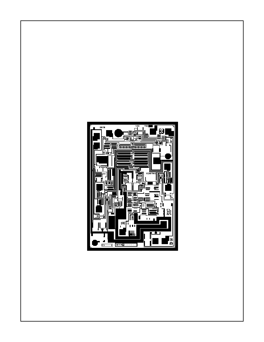
Die Characteristics
DIE DIMENSIONS:
71 mils x 100 mils x 19 mils
METALLIZATION:
Type: Aluminum, 1% Copper
Thickness: 16k
≈
±
2k
≈
SUBSTRATE POTENTIAL
V-
PASSIVATION:
Type: Nitride (Si
3
N
4
) over Silox (SiO
2
, 5% Phos)
Nitride Thickness: 3.5k
≈
±
2k
≈
Silox Thickness: 12k
≈
±
2k
≈
TRANSISTOR COUNT:
72
PROCESS:
Bipolar Dielectric Isolation
Metallization Mask Layout
HA-2557
GND
1
V
REF
2
3
4
V
Y
+
V
Y
-
V-
7
I
OUT
8
R
Z
10
11
12
13
V
XIO
B
15
V
XIO
A
16
V
YIO
B
V
YIO
A
5
6
V+
V
X
-
V
X
+
V
Z
+
9