 | –≠–ª–µ–∫—Ç—Ä–æ–Ω–Ω—ã–π –∫–æ–º–ø–æ–Ω–µ–Ω—Ç: HA-2850 | –°–∫–∞—á–∞—Ç—å:  PDF PDF  ZIP ZIP |
1
CAUTION: These devices are sensitive to electrostatic discharge; follow proper IC Handling Procedures.
1-888-INTERSIL or 321-724-7143
|
Copyright
©
Intersil Corporation 1999
HA-2850
470MHz, Low Power, High Slew Rate
Operational Amplifier
The HA-2850 is a wideband, high slew rate, operational
amplifier featuring superior speed and bandwidth
characteristics. Bipolar construction, coupled with dielectric
isolation, delivers outstanding performance in circuits with a
closed loop gain of 10 or greater.
A 340V/
µ
s slew rate and a 470MHz gain bandwidth product
ensure high performance in video and wideband amplifier
designs. Differential gain and phase are a low 0.04% and
0.04 degrees respectively, making the HA-2850 ideal for
video applications. A full
±
10V output swing, high open loop
gain, and outstanding AC parameters, make the HA-2850 an
excellent choice for high speed Data Acquisition Systems.
For military grade product, refer to the HA-2850/883 data
sheet. Intersil AnswerFAX (321-724-7800) Document #3595.
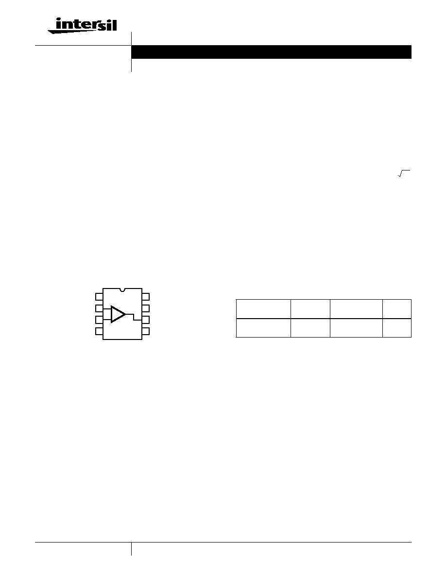
Pinout
HA-2850
(SOIC)
TOP VIEW
Features
∑ Low Supply Current . . . . . . . . . . . . . . . . . . . . . . . . 7.5mA
∑ High Slew Rate. . . . . . . . . . . . . . . . . . . . . . . . . . . 340V/
µ
s
∑ Open Loop Gain . . . . . . . . . . . . . . . . . . . . . . . . . . 25kV/V
∑ Wide Gain-Bandwidth (A
V
10) . . . . . . . . . . . . . . 470MHz
∑ Full Power Bandwidth . . . . . . . . . . . . . . . . . . . . . . 5.4MHz
∑ Low Offset Voltage . . . . . . . . . . . . . . . . . . . . . . . . . 0.6mV
∑ Input Noise Voltage . . . . . . . . . . . . . . . . . . . .
∑ Differential Gain/Phase. . . . . . . . . . . 0.04%/0.04 Degrees
∑ Lower Power Enhanced Replacement for AD840 and
EL2040
Applications
∑ Pulse and Video Amplifiers
∑ Wideband Amplifiers
∑ High Speed Sample-Hold Circuits
∑ Fast, Precise D/A Converters
NC
-IN
+IN
V-
1
2
3
4
8
7
6
5
NC
V+
OUT
NC
-
+
Ordering Information
PART NUMBER
(BRAND)
TEMP.
RANGE (
o
C)
PACKAGE
PKG.
NO.
HA9P2850-5
(H28505)
0 to 75
8 Ld SOIC
M8.15
11nV
/
Hz
Data Sheet
September 1998
File Number
2844.4

2
Absolute Maximum Ratings
Thermal Information
Voltage Between V+ and V- Terminals. . . . . . . . . . . . . . . . . . . . 35V
Differential Input Voltage . . . . . . . . . . . . . . . . . . . . . . . . . . . . . . . 6V
Operating Conditions
Temperature Range
HA-2850-5 . . . . . . . . . . . . . . . . . . . . . . . . . . . . . . . . 0
o
C to 75
o
C
Recommended Supply Voltage Range . . . . . . . . . . . .
±
6V To
±
15V
Thermal Resistance (Typical, Note 1)
JA
(
o
C/W)
8 Ld SOIC Package . . . . . . . . . . . . . . . . . . . . . . . . .
157
Maximum Junction Temperature (Die) . . . . . . . . . . . . . . . . . . . .175
o
C
Maximum Junction Temperature (Plastic Package, Note 2) . .150
o
C
Maximum Storage Temperature Range . . . . . . . . . . -65
o
C to 150
o
C
Maximum Lead Temperature (Soldering 10s) . . . . . . . . . . . . 300
o
C
(SOIC - Lead Tips Only)
CAUTION: Stresses above those listed in "Absolute Maximum Ratings" may cause permanent damage to the device. This is a stress only rating and operation of the
device at these or any other conditions above those indicated in the operational sections of this specification is not implied.
NOTES:
1.
JA
is measured with the component mounted on an evaluation PC board in free air.
2. Maximum power dissipation, including output load, must be designed to maintain the maximum junction temperature below 150
o
C for plastic
packages.
Electrical Specifications
V
SUPPLY
=
±
15V, R
L
= 1k
, C
L
10pF, Unless Otherwise Specified
PARAMETER
TEST CONDITIONS
TEMP. (
o
C)
HA-2850-5
UNITS
MIN
TYP
MAX
INPUT CHARACTERISTICS
Offset Voltage (Note 9)
25
-
0.6
2
mV
Full
-
2
6
mV
Average Offset Voltage Drift
Full
-
20
-
µ
V/
o
C
Bias Current (Note 9)
25
-
5
14.5
µ
A
Full
-
8
20
µ
A
Offset Current
25
-
1
4
µ
A
Full
-
-
8
µ
A
Input Resistance
25
-
10
-
k
Input Capacitance
25
-
1
-
pF
Common Mode Range
Full
±
10
-
-
V
Input Noise Voltage (Note 9)
f = 1kHz, R
SOURCE
= 0
25
-
11
-
Input Noise Current (Note 9)
f = 1kHz, R
SOURCE
= 10k
25
-
6
-
TRANSFER CHARACTERISTICS
Large Signal Voltage Gain
Note 4
25
20
25
-
kV/V
Full
15
20
-
kV/V
Common-Mode Rejection Ratio (Note 9)
V
CM
=
±
10V
Full
75
80
-
dB
Minimum Stable Gain
25
10
-
-
V/V
Gain Bandwidth Product (Note 9)
V
O
= 90mV, A
V
= 100
25
-
470
-
MHz
OUTPUT CHARACTERISTICS
Output Voltage Swing (Note 9)
Note 4
Full
±
10
±
11
-
V
Output Current (Note 9)
Note 4
Full
±
10
±
20
-
mA
Output Resistance
25
-
30
-
Full Power Bandwidth (Note 5)
Note 4
25
4.8
5.4
-
MHz
Differential Gain
A
V
= +10, Note 3
25
-
0.04
-
%
Differential Phase
A
V
= +10, Note 3
25
-
0.04
-
Degrees
Harmonic Distortion (Note 9)
A
V
= +10, V
O
= 2V
P-P
, f = 1MHz
25
-
-74
-
dBc
nV Hz
/
pA
Hz
/
HA-2850
3
TRANSIENT RESPONSE (Note 6)
Rise Time
25
-
5
-
ns
Overshoot
25
-
25
-
%
Slew Rate (Notes 8, 9)
Note 4
25
300
340
-
V/
µ
s
Settling Time
10V Step to 0.1%
25
-
200
-
ns
POWER REQUIREMENTS
Supply Current (Note 9)
Full
-
7.5
8.0
mA
Power Supply Rejection Ratio (Note 9)
Note 7
Full
75
90
-
dB
NOTES:
3. Differential gain and phase are measured with a VM700A video tester, using a NTC-7 composite VITS.
4. R
L
= 1k
, V
O
=
±
10V, 0V to
±
10V for slew rate.
5. Full Power Bandwidth guaranteed based on slew rate measurement using:
.
6. Refer to Test Circuit section of data sheet.
7. V
SUPPLY
=
±
10V to
±
20V.
8. This parameter is not tested. The limits are guaranteed based on lab characterization, and reflect lot-to-lot variation.
9. See "Typical Performance Curves" for more information.
Electrical Specifications
V
SUPPLY
=
±
15V, R
L
= 1k
, C
L
10pF, Unless Otherwise Specified (Continued)
PARAMETER
TEST CONDITIONS
TEMP. (
o
C)
HA-2850-5
UNITS
MIN
TYP
MAX
FPBW
Slew Rate
2
V
PEAK
---------------------------
V
PEAK
10V
=
;
=
Test Circuits and Waveforms
TEST CIRCUIT
LARGE SIGNAL RESPONSE
SMALL SIGNAL RESPONSE
IN
OUT
+
900
100
-
NOTES:
10. V
S
=
±
15V.
11. A
V
= +10.
12. C
L
< 10pF.
INPUT
OUTPUT
Input = 1V/Div.
Output = 5V/Div.
50ns/Div.
INPUT
OUTPUT
Input = 10mV/Div.
Output = 100mV/Div.
50ns/Div.
HA-2850
4
SETTLING TIME TEST CIRCUIT
Test Circuits and Waveforms
(Continued)
+
V-
0.001
µ
F
0.001
µ
F
1
µ
F
1
µ
F
2k
5k
V+
INPUT
500
SETTLING
POINT
200
OUTPUT
PROBE
MONITOR
-
NOTES:
13. A
V
= -10.
14. Load Capacitance should be less than 10pF.
15. It is recommended that resistors be carbon composition and that
feedback and summing network ratios be matched to 0.1%.
16. SETTLING POINT (Summing Node) capacitance should be less
than 10pF. For optimum settling time results, it is recommended
that the test circuit be constructed directly onto the device pins.
A Tektronix 568 Sampling Oscilloscope with S-3A sampling
heads is recommended as a settle point monitor.
Typical Performance Curves
T
A
= 25
o
C, V
SUPPLY
=
±
15V, R
L
= 1k
, C
L
< 10pF, Unless Otherwise Specified
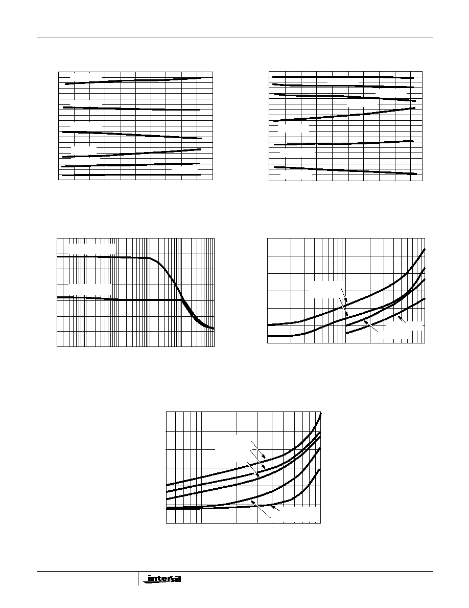
FIGURE 1. FREQUENCY RESPONSE FOR VARIOUS GAINS
FIGURE 2. GAIN BANDWIDTH PRODUCT vs SUPPLY VOLTAGE
FIGURE 3. GAIN BANDWIDTH PRODUCT vs TEMPERATURE
FIGURE 4. CMRR vs FREQUENCY
100
80
60
40
20
0
OPEN LOOP
A
VCL
= 1000
A
VCL
= 100
A
VCL
= 10
A
VCL
= 1000
A
VCL
= 100
A
VCL
= 10
OPEN LOOP
10K
100K
1M
10M
100M 500M
FREQUENCY (Hz)
GAIN (dB)
0
90
180
PHASE (DEGREES)
1K
475
450
425
400
GAIN B
AND
WIDTH PR
ODUCT (MHz)
5
6
7
8
9
10
11
12
13
14
15
SUPPLY VOLTAGE (
±
V)
600
500
400
300
200
GAIN B
AND
WIDTH
PR
ODUCT (MHz)
-60
-40
-20
0
20
40
60
80
100
120
140
TEMPERATURE (
o
C)
250
350
450
550
100
10K
100K
1M
10M
FREQUENCY (Hz)
1K
90
80
70
60
50
40
30
20
CMRR (dB)
HA-2850
5
FIGURE 5. PSRR vs FREQUENCY
FIGURE 6. INPUT NOISE vs FREQUENCY
FIGURE 7. SLEW RATE vs TEMPERATURE
FIGURE 8. SLEW RATE vs SUPPLY VOLTAGE
FIGURE 9. INPUT OFFSET VOLTAGE AND INPUT BIAS
CURRENT vs TEMPERATURE
FIGURE 10. SUPPLY CURRENT vs SUPPLY VOLTAGE
Typical Performance Curves
T
A
= 25
o
C, V
SUPPLY
=
±
15V, R
L
= 1k
, C
L
< 10pF, Unless Otherwise Specified (Continued)
100
10K
100K
1M
10M
FREQUENCY (Hz)
1K
100
90
80
70
60
50
40
30
20
10
0
110
PSRR (dB)
±
PSRR
60
50
40
30
20
10
0
NOISE V
O
L
T
A
GE (nV/
Hz)
10
100
1K
10K
100K
NOISE CURRENT
NOISE VOLTAGE
FREQUENCY (Hz)
60
50
40
30
20
10
0
NOISE CURRENT (pA/
Hz)
350
325
300
275
250
SLEW RA
TE (V/
µ
s)
-60
-40
-20
0
20
40
60
80
100
120
140
TEMPERATURE (
o
C)
225
325
300
275
250
225
SLEW RA
TE (V/
µ
s)
5
6
7
8
9
10
11
12
13
14
15
SUPPLY VOLTAGE (
±
V)
350
6.5
6.0
5.5
5.0
4.5
4.0
-60
-40
-20
0
20
40
60
80
100 120
140
3.5
2.5
1.5
0.5
-0.5
INPUT OFFSET V
O
L
T
A
GE (mV)
BIAS CURRENT
OFFSET VOLTAGE
TEMPERATURE (
o
C)
INPUT BIAS CURRENT (
µ
A)
8.0
7.5
7.0
6.5
6.0
5.5
5.0
SUPPL
Y CURRENT (mA)
5
6
7
8
9
10
11
12
13
14
15
SUPPLY VOLTAGE (
±
V)
125
o
C
25
o
C
-55
o
C
HA-2850
6
FIGURE 11. POSITIVE OUTPUT SWING vs TEMPERATURE
FIGURE 12. NEGATIVE OUTPUT SWING vs TEMPERATURE
FIGURE 13. MAXIMUM UNDISTORTED OUTPUT SWING vs
FREQUENCY
FIGURE 14. TOTAL HARMONIC DISTORTION vs FREQUENCY
FIGURE 15. INTERMODULATION DISTORTION vs FREQUENCY (TWO TONE)
Typical Performance Curves
T
A
= 25
o
C, V
SUPPLY
=
±
15V, R
L
= 1k
, C
L
< 10pF, Unless Otherwise Specified (Continued)
13
9
5
POSITIVE OUTPUT SWING (V)
-60
-40
-20
0
20
40
60
80
100 120
140
TEMPERATURE (
o
C)
3
7
11
±
8V, 75
±
15V, 1k
±
15V, 150
±
8V, 1k
±
8V, 150
±
15V, 75
-60
-40
-20
0
20
40
60
80
100
120 140
TEMPERATURE (
o
C)
NEGA
TIVE OUTPUT SWING (V)
-3
-7
-11
-13
-5
-9
±
8V, 75
±
15V, 75
±
15V, 1k
±
15V, 150
±
8V, 1k
±
8V, 150
30
25
20
15
10
5
0
OUTPUT V
O
L
T
A
GE SWING (V
P-P
)
1K
10K
100K
1M
10M
100M
FREQUENCY (Hz)
V
SUPPLY
=
±
8V
V
SUPPLY
=
±
15V
100K
1M
10M
-40
-50
-60
-70
-80
-90
FREQUENCY (Hz)
V
O
= 2V
P-P
V
O
= 0.5V
P-P
THD (dBc)
-30
V
O
= 10V
P-P
V
O
= 1V
P-P
V
O
= 0.25V
P-P
V
O
= 0.5V
P-P
V
O
= 2V
P-P
V
O
= 5V
P-P
V
O
= 1V
P-P
-90
-80
-70
-60
-50
-40
-30
3RD INTERMOD PR
ODUCT (dBc)
500K
1M
10M
FREQUENCY (Hz)
HA-2850
7
All Intersil semiconductor products are manufactured, assembled and tested under ISO9000 quality systems certification.
Intersil semiconductor products are sold by description only. Intersil Corporation reserves the right to make changes in circuit design and/or specifications at any time with-
out notice. Accordingly, the reader is cautioned to verify that data sheets are current before placing orders. Information furnished by Intersil is believed to be accurate and
reliable. However, no responsibility is assumed by Intersil or its subsidiaries for its use; nor for any infringements of patents or other rights of third parties which may result
from its use. No license is granted by implication or otherwise under any patent or patent rights of Intersil or its subsidiaries.
For information regarding Intersil Corporation and its products, see web site http://www.intersil.com
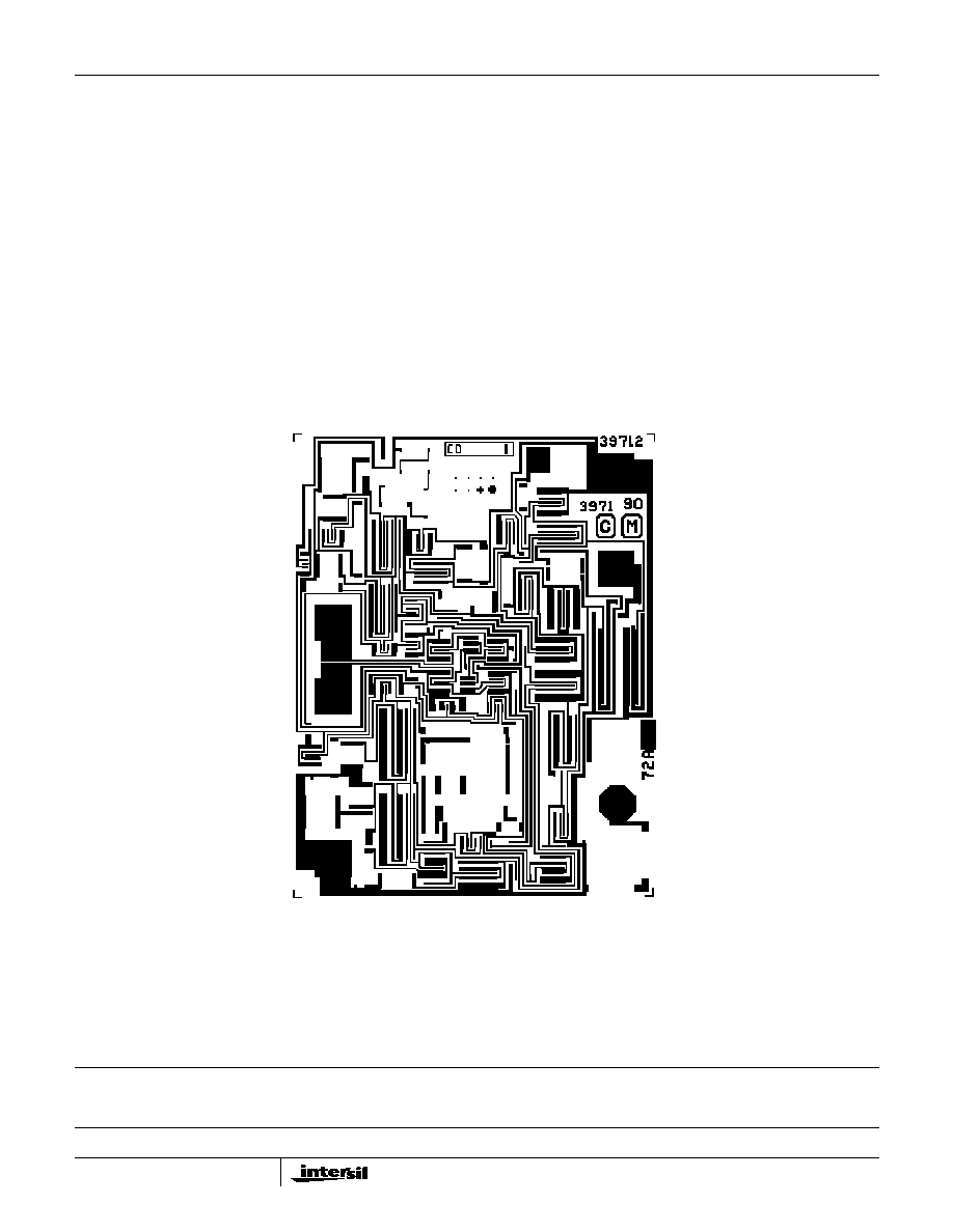
Die Characteristics
DIE DIMENSIONS:
65 mils x 52 mils x 19 mils
1650
µ
m x 1310
µ
m x 483
µ
m
METALLIZATION:
Type: Aluminum, 1% Copper
Thickness: 16k
≈
±
2k
≈
SUBSTRATE POTENTIAL
V-
PASSIVATION:
Type: Nitride over Silox
Silox Thickness: 12k
≈
±
2k
≈
Nitride Thickness: 3.5k
≈
±
1k
≈
TRANSISTOR COUNT:
34
PROCESS:
High Frequency Bipolar Dielectric Isolation
Metallization Mask Layout
HA-2850
V-
+IN
-IN
OUT
V+
HA-2850