244
TM
HA-2850/883
Low Power, High Slew Rate,
Wideband Operational Amplifier
Description
The HA-2850/883 is a wideband, high slew rate, operational
amplifier featuring superior speed and bandwidth
characteristics. It also features trimmed supply current,
which minimizes supply current (and thus AC parameter)
variation over process and temperature extremes. For exam-
ple, the I
CC
variation over the entire military temperature
range is typically less than 0.5mA. Bipolar construction, cou-
pled with dielectric isolation, delivers outstanding perfor-
mance in circuits with closed loop gains
10.
The 340V/
µ
s slew rate, and 470MHz gain bandwidth product
ensure high performance in video and wideband amplifier
designs. Differential gain and phase are a low 0.04% and
0.04 degrees, respectively, making the HA-2850/883 ideal
for video applications. A full
±
10V output swing, high open
loop gain, and outstanding AC parameters make the
HA-2850/883 an excellent choice for data acquisition
systems.
Ordering Information
PART
NUMBER
TEMPERATURE
RANGE
PACKAGE
HA1-2850/883
-55
o
C to +125
o
C
14 Lead CerDIP
HA7-2850/883
-55
o
C to +125
o
C
8 Lead CerDIP
Features
∑ This Circuit is Processed in Accordance to MIL-STD-
883 and is Fully Conformant Under the Provisions of
Paragraph 1.2.1.
∑ Low Supply Current. . . . . . . . . . . . . . . . . . 8.0mA (Max)
∑ Low Offset Voltage . . . . . . . . . . . . . . . . . . .2.0mV (Max)
∑ High Slew Rate . . . . . . . . . . . . . . . . . . . . . 340V/
µ
s (Typ)
∑ Open Loop Gain . . . . . . . . . . . . . . . . . . . . . 20kV/V (Min)
∑ Wide Gain-Bandwidth (A
V
10) . . . . . . . 470MHz (Typ)
∑ Input Noise Voltage at 1kHz . . . . . . . . . 11nV/
Hz (Typ)
∑ Lower Power Replacement for HA-2540/883, AD840
Applications
∑ Pulse and Video Amplifiers
∑ Wideband Amplifiers
∑ High Speed Sample-Hold Circuits
∑ Fast, Precise D/A Converters
July 1994
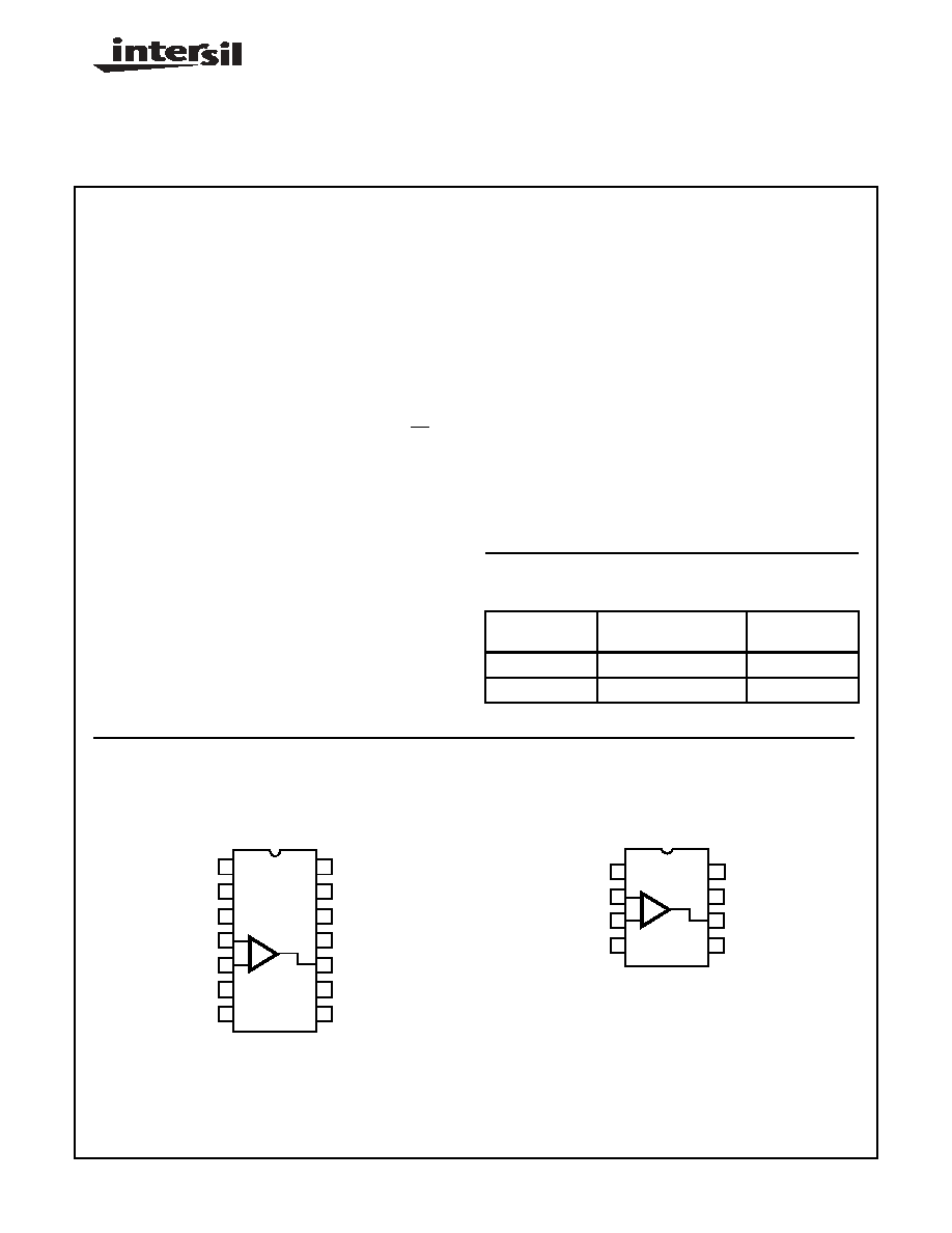
Pinouts
HA-2850/883
(CERDIP)
TOP VIEW
HA-2850/883
(CERDIP)
TOP VIEW
NC
NC
V+
NC
OUT
1
2
3
4
5
6
7
14
13
12
11
10
9
8
+
NC
NC
NC
-IN
+IN
V -
NC
NC
NC
-
NC
V+
OUT
1
2
3
4
8
7
6
5
+
-
NC
-IN
+IN
V -
NC
Spec Number
511095-883
FN3595.1
CAUTION: These devices are sensitive to electrostatic discharge; follow proper IC Handling Procedures.
1-888-INTERSIL or 321-724-7143
|
Intersil (and design) is a trademark of Intersil Americas Inc.
Copyright © Intersil Americas Inc. 2002. All Rights Reserved
245
Specifications HA-2850/883
Absolute Maximum Ratings
Thermal Information
Voltage between V+ and V- Terminals. . . . . . . . . . . . . . . . . . . . 35V
Differential Input Voltage . . . . . . . . . . . . . . . . . . . . . . . . . . . . . . . 6V
Voltage at Either Input Terminal. . . . . . . . . . . . . . . . . . . . . . V+ to V-
Peak Output Current (
10% Duty Cycle) . . . . . . . . . . . . . . . . . 50mA
Junction Temperature (T
J
) . . . . . . . . . . . . . . . . . . . . . . . . . . +175
o
C
Storage Temperature Range . . . . . . . . . . . . . . . . . -65
o
C to +150
o
C
ESD Classification . . . . . . . . . . . . . . . . . . . . . . . . . . . . . . . . <2000V
Lead Temperature (Soldering 10s). . . . . . . . . . . . . . . . . . . . +300
o
C
Thermal Resistance
JA
J
C
14 Lead CerDIP Package . . . . . . . . . . . .
81
o
C/W
26
o
C/W
8 Lead CerDIP Package . . . . . . . . . . . . .
115
o
C/W
30
o
C/W
Package Power Dissipation Limit at +75
o
C for T
J
+175
o
C
14 Lead CerDIP Package . . . . . . . . . . . . . . . . . . . . . . . . . . 1.23W
8 Lead CerDIP Package . . . . . . . . . . . . . . . . . . . . . . . . . . . 0.87W
Package Power Dissipation Derating Factor Above +75
o
C
14 Lead CerDIP Package . . . . . . . . . . . . . . . . . . . . . .12.3mW/
o
C
8 Lead CerDIP Package . . . . . . . . . . . . . . . . . . . . . . . . 8.7mW/
o
C
CAUTION: Stresses above those listed in "Absolute Maximum Ratings" may cause permanent damage to the device. This is a stress only rating and operation
of the device at these or any other conditions above those indicated in the operational sections of this specification is not implied.
Operating Conditions
Operating Temperature Range. . . . . . . . . . . . . . . . -55
o
C to +125
o
C
Operating Supply Voltage
. . . . . . . . . . . . . . . . . . . . . . . . . ±
12V to
±
15V
V
INCM
1/2 (V+ - V-)
R
L
1k
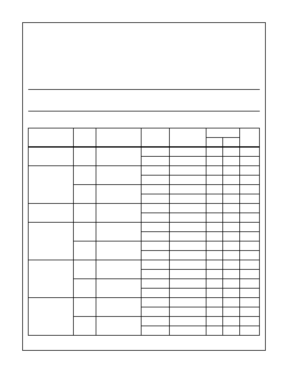
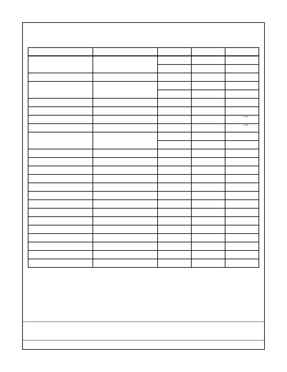
TABLE 1. DC ELECTRICAL PERFORMANCE CHARACTERISTICS
Device Tested at: V
SUPPLY
=
±
15V, R
SOURCE
= 100
, R
LOAD
= 100k
, V
OUT
= 0V, Unless Otherwise Specified.
PARAMETERS
SYMBOL
CONDITIONS
GROUP A
SUBGROUP
TEMPERATURE
LIMITS
UNITS
MIN
MAX
Input Offset Voltage
V
IO
V
CM
= 0V
1
+25
o
C
-2
2
mV
2, 3
+125
o
C, -55
o
C
-6
6
mV
Input Bias Current
+I
B
V
CM
= 0V, +R
S
= 1.1k
-R
S
= 100
1
+25
o
C
-14.5
14.5
µ
A
2, 3
+125
o
C, -55
o
C
-20
20
µ
A
-I
B
V
CM
= 0V, +R
S
= 100
-R
S
= 1.1k
1
+25
o
C
-14.5
14.5
µ
A
2, 3
+125
o
C, -55
o
C
-20
20
µ
A
Input Offset Current
I
IO
V
CM
= 0V, +R
S
= 1.1k
-R
S
= 1.1k
1
+25
o
C
-4
4
µ
A
2, 3
+125
o
C, -55
o
C
-8
8
µ
A
Common Mode Range
+CMR
V+ = 5V, V- = -25V
1
+25
o
C
10
-
V
2, 3
+125
o
C, -55
o
C
10
-
V
-CMR
V+ = 25V, V- = -5V
1
+25
o
C
-
-10
V
2, 3
+125
o
C, -55
o
C
-
-10
V
Large Signal Voltage
Gain
+A
VOL
V
OUT
= 0V and +10V
R
L
= 1k
4
+25
o
C
20
-
kV/V
5, 6
+125
o
C, -55
o
C
10
-
kV/V
-A
VOL
V
OUT
= 0V and -10V
R
L
= 1k
4
+25
o
C
20
-
kV/V
5, 6
+125
o
C, -55
o
C
10
-
kV/V
Common Mode
Rejection Ratio
+CMRR
V
CM
= 10V,
V
OUT
= -10V
V+ = 5V, V- = -25V
1
+25
o
C
75
-
dB
2,3 +125
o
C, -55
o
C
75
-
dB
-CMRR
V
CM
= -10V,
V
OUT
= 10V
V+ = 25V, V- = -5V
1
+25
o
C
75
-
dB
2, 3
+125
o
C, -55
o
C
75
-
dB
Spec Number
511095-883

246
Specifications HA-2850/883
Output Voltage Swing
+V
OUT
R
L
= 1k
1
+25
o
C
10
-
V
2, 3
+125
o
C, -55
o
C
10
-
V
-V
OUT
R
L
= 1k
1
+25
o
C
-
-10
V
2, 3
+125
o
C, -55
o
C
-
-10
V
Output Current
+I
OUT
V
OUT
= 10V
1
+25
o
C
10
-
mA
2, 3
+125
o
C, -55
o
C
10
-
mA
-I
OUT
V
OUT
= -10V
1
+25
o
C
-
-10
mA
2, 3
+125
o
C, -55
o
C
-
-10
mA
Quiescent Power
Supply Current
+I
CC
V
OUT
= 0V, I
OUT
= 0mA
1
+25
o
C
-
8
mA
2, 3
+125
o
C, -55
o
C
-
8
mA
-I
CC
V
OUT
= 0V, I
OUT
= 0mA
1
+25
o
C
-8
-
mA
2, 3
+125
o
C, -55
o
C
-8
-
mA
Power Supply
Rejection Ratio
+PSRR
V
SUP
= 10V
V+ = 10V, V- = -15V
V+ = 20V, V- = -15V
1
+25
o
C
75
-
dB
2, 3
+125
o
C, -55
o
C
75
-
dB
-PSRR
V
SUP
= 10V
V+ = 15V, V- = -10V
V+ = 15V, V- = -20V
1
+25
o
C
75
-
dB
2, 3
+125
o
C, -55
o
C
75
-
dB
TABLE 2. AC ELECTRICAL PERFORMANCE CHARACTERISTICS
Table 2 Intentionally Left Blank. See A.C. Specifications in Table 3
TABLE 1. DC ELECTRICAL PERFORMANCE CHARACTERISTICS (Continued)
Device Tested at: V
SUPPLY
=
±
15V, R
SOURCE
= 100
, R
LOAD
= 100k
, V
OUT
= 0V, Unless Otherwise Specified.
PARAMETERS
SYMBOL
CONDITIONS
GROUP A
SUBGROUP
TEMPERATURE
LIMITS
UNITS
MIN
MAX
Spec Number
511095-883

247
Specifications HA-2850/883
TABLE 3. ELECTRICAL PERFORMANCE CHARACTERISTICS
Device Characterized at: V
SUPPLY
=
±
15V, R
SOURCE
= 50
, R
LOAD
= 1k
, C
L
10pF, A
V
= +10V/V, Unless Otherwise Specified.
PARAMETERS
SYMBOL
CONDITIONS
NOTES
TEMPERATURE
LIMITS
UNITS
MIN
MAX
Gain Bandwidth
Product
GBWP
V
O
= 200mV, f
O
= 5MHz
1
+25
o
C
400
-
MHz
V
O
= 200mV,
f
O
= 45MHz
1
+25
o
C
350
-
MHz
Slew Rate
+SR
V
O
= -5V to +5V
1, 4
+25
o
C
300
-
V/
µ
s
-SR
V
O
= +5V to -5V
1, 4
+25
o
C
300
-
V/
µ
s
Full Power Bandwidth
FPBW
V
PEAK
= 10V
1, 2
+25
o
C
4.8
-
MHz
Rise and Fall Time
T
R
V
O
= 0V to +200mV
1, 4
+25
o
C
-
15
ns
T
F
V
O
= 0V to -200mV
1, 4
+25
o
C
-
15
ns
Minimum Closed Loop
Stable Gain
CLSG
R
L
= 1k
,
C
L
10pF
1
-55
o
C to +125
o
C
10
-
V/V
Overshoot
+OS
V
O
= 0V to +200mV
1
+25
o
C
-
30
%
-OS
V
O
= 0V to -200mV
1
+25
o
C
-
30
%
Open Loop Output
Resistance
R
OUT
V
OUT
= 0V
1
+25
o
C
-
60
Quiescent Power
Consumption
PC
V
OUT
= 0V, I
OUT
= 0mA
1, 3
-55
o
C to +125
o
C
-
240
mW
NOTES:
1. Parameters listed in Table 3 are controlled via design or process parameters and are not directly tested at final production. These param-
eters are lab characterized upon initial design release, or upon design changes. These parameters are guaranteed by characterization
based upon data from multiple production runs which reflect lot to lot and within lot variation.
2. Full Power Bandwidth guarantee based on Slew Rate measurement using FPBW = Slew Rate/(2
V
PEAK
).
3. Quiescent Power Consumption based upon Quiescent Supply Current test maximum. (No load on outputs.)
4. Measured between 10% and 90% points.
TABLE 4. ELECTRICAL TEST REQUIREMENTS
MIL-STD-883 TEST REQUIREMENTS
SUBGROUPS (SEE TABLE 1)
Interim Electrical Parameters (Pre Burn-In)
1
Final Electrical Test Parameters
1 (Note 1), 2, 3, 4, 5, 6
Group A Test Requirements
1, 2, 3, 4, 5, 6
Groups C and D Endpoints
1
NOTE:
1. PDA applies to Subgroup 1 only.
Spec Number
511095-883
248
Spec Number
511095-883
HA-2850/883
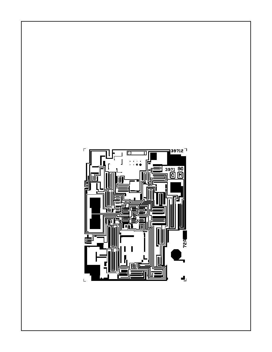
Die Characteristics
DIE DIMENSIONS:
65 x 52 x 19 mils
±
1 mils
1650 x 1310 x 483
µ
m
±
25.4
µ
m
METALLIZATION:
Type: Al, 1% Cu
Thickness: 16k
≈
±
2k
≈
GLASSIVATION:
Type: Nitride over Silox
Silox Thickness: 12k
≈
±
2k
≈
Nitride Thickness: 3.5k
≈
±
1.5k
≈
WORST CASE CURRENT DENSITY:
0.7 x 10
5
A/cm
2
at 1.8mA
SUBSTRATE POTENTIAL (Powered Up): V-
TRANSISTOR COUNT: 34
PROCESS: Bipolar Dielectric Isolation
Metallization Mask Layout
HA-2850/883
V-
+IN
-IN
OUT
V+
249
HA-2850/883
Test Circuit
(Applies to Table 1)
Test Waveforms
SIMPLIFIED TEST CIRCUIT FOR LARGE AND SMALL SIGNAL RESPONSE (APPLIES TO TABLE 3)
MEASURED LARGE SIGNAL RESPONSE
Vertical Scale: Input = 1V/Div., Output = 5V/Div.
Horizontal Scale: 50ns /Div.
MEASURED SMALL SIGNAL RESPONSE
Vertical Scale: Input = 10mV/Div., Output=100mV/Div.
Horizontal Scale: 50ns/Div.
S5A
1
100
+V
CC
S5B 1
+
1
2
3
S8
1K
10K
-V
EE
OPEN
S9
1
2
1
V2
E
OUT
1
1K
S1
S2
S6
1
DUT
1
0.1
S7
100K
FOR LOOP STABILITY,
USE MIN VALUE CAPACITOR
TO PREVENT OSCILLATION
OPEN 2
OPEN 2
1K
ALL RESISTORS =
±
1% (
)
ALL CAPACITORS =
±
10% (
µ
F)
0.1
1
+
2
10K
100K
V1
BUFFER
OPEN
1
OPEN
OPEN
2 OPEN
100
2
OPEN
F B
-1
V
IN
V
OUT
+
900
100
-
50
NOTES:
1. V
S
=
±
15V
2. A
V
= +10
3. C
L
10pF
INPUT
OUTPUT
INPUT
OUTPUT
Spec Number
511095-883
250
HA-2850/883
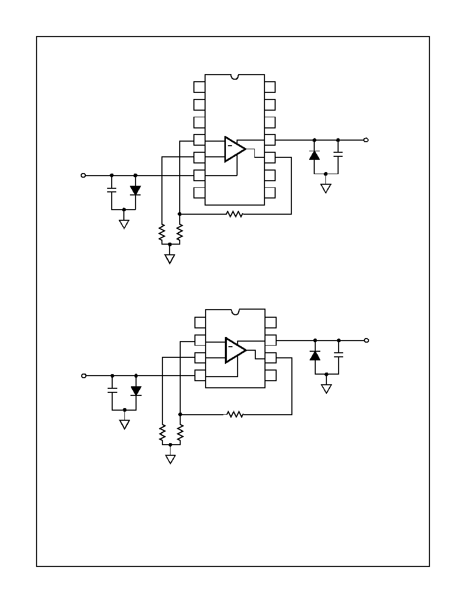
Burn-In Circuits
HA1-2850/883 CERAMIC DIP
HA7-2850/883 CERAMIC DIP
NOTES:
1. R
1
= 1k
,
±
5%, 1/4W (Min)
2. R
2
= 1k
,
±
5%, 1/4W (Min)
3. R
3
= 10k
,
±
5%, 1/4W (Min)
4. C
1
= C
2
= 0.01
µ
F/Socket (Min) or 0.1
µ
F/Row, (Min)
5. D
1
= D
2
= 1N4002 or Equivalent/Board
6.
(V+) - (V-)
= 31V
±
1V
1
2
3
4
5
6
7
14
13
12
11
10
9
8
+
C
2
D
2
R
1
R
2
R
3
D
1
C
1
V+
V-
1
2
3
4
8
7
6
5
+
C
2
D
2
R
1
R
2
R
3
D
1
C
1
V+
V-
Spec Number
511095-883
251
HA-2850/883
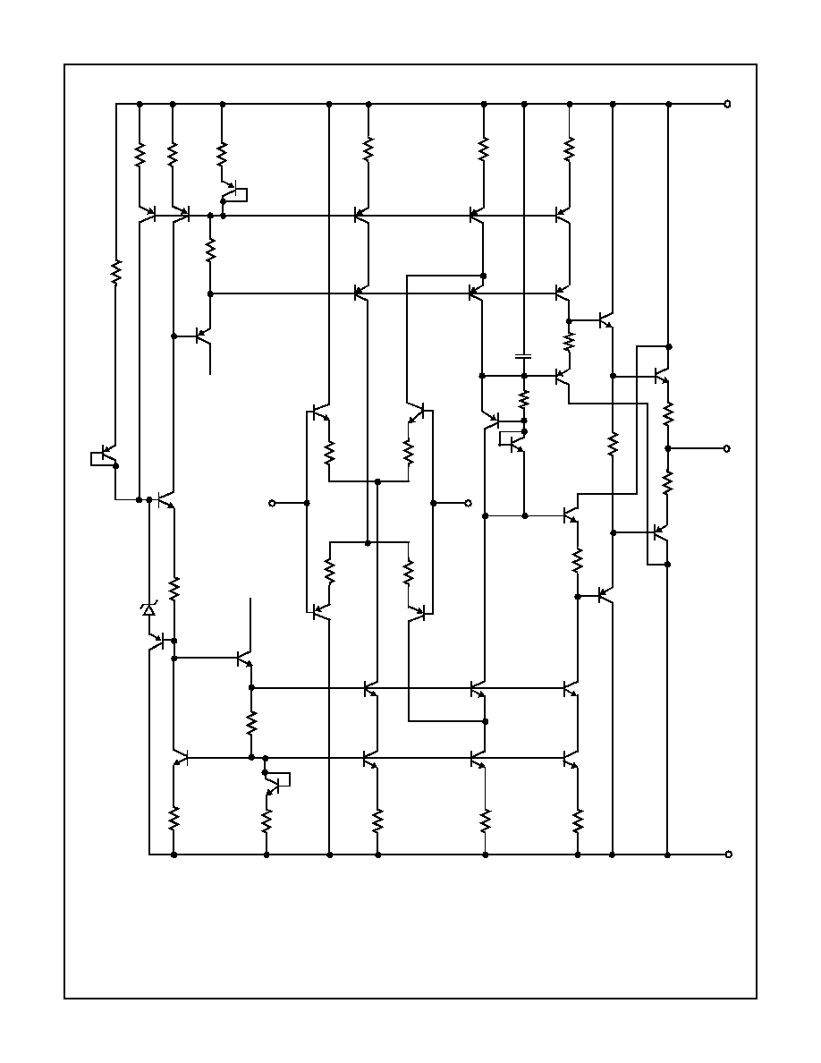
Schematic Diagram
QN5
R1
250K
R2
3K
R3
1.4K
R4
1.4K
R5
3K
QP3
QP4
QP5
QP6
QP1
QN1
R6
DZ1
QP2
QN3
QN2
R8
3K
QN4
R7
1.4K
R9
1.4K
R10
190
QP8
QN6
R11
40
R12
40
R13
40
R14
40
QP10
QN7
QN8
R15
190
R16
R17
500
QP11
QP13
QN9
R19
3K
C
C
1.8pF
QP14
QP12
QP15
QN15
QP16
R23
6K
R24
35
R25
35
QP18
QN16
R18
10
QN12
R20
10
QP17
QN10
QN11
QN14
R21
R22
500
+IN
-IN
QP7
QP9
QN13
V-
V+
V+
190
OUT
V-
190
19K
Spec Number
511095-883
The information contained in this section has been developed through characterization by Intersil Corporation and is for use as application
and design information only. No guarantee is implied.
252
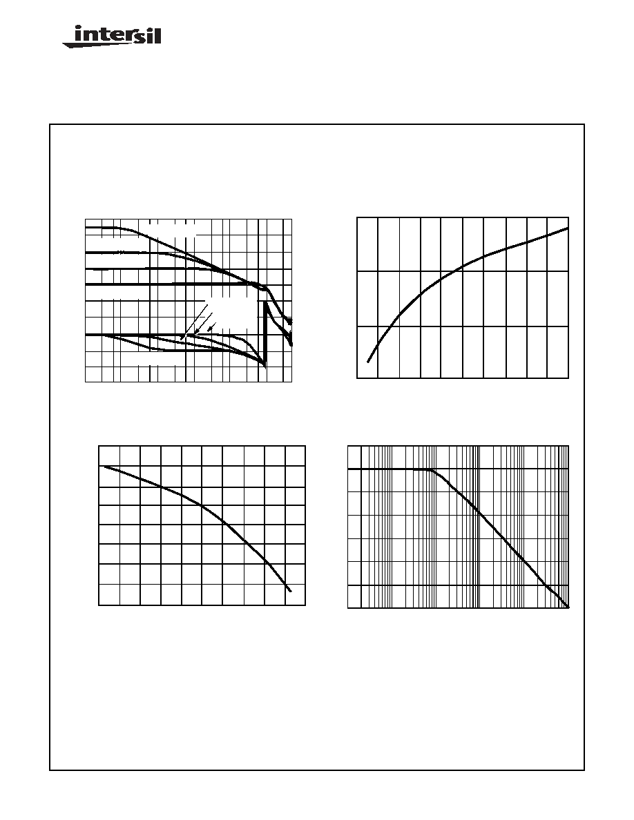
DESIGN INFORMATION
TM
HA-2850
Low Power, High Slew Rate,
Wideband Operational Amplifier
Typical Performance Curves
V
SUPPLY
=
±
15V, A
V
= +10, R
L
= 1k
, C
L
10pF, T
A
= +25
o
C, Unless Otherwise Specified
FREQUENCY RESPONSE FOR VARIOUS GAINS
GAIN BANDWIDTH PRODUCT vs SUPPLY VOLTAGE
GAIN BANDWIDTH PRODUCT vs TEMPERATURE
CMRR vs FREQUENCY
100
80
60
40
20
0
OPEN LOOP
A
VCL
= 1000
A
VCL
= 100
A
VCL
= 10
A
VCL
= 1000
A
VCL
= 100
A
VCL
= 10
OPEN LOOP
10K
100K
1M
10M
100M 500M
FREQUENCY (Hz)
G
A
IN (
d
B)
0
90
180
PH
A
S
E (
D
EG
R
E
E
S
)
1K
475
450
425
400
G
A
IN BANDW
IDT
H
P
R
O
DUCT
(
M
Hz
)
5
6
7
8
9
10
11
12
13
14
15
SUPPLY VOLTAGE (
±
V
)
600
500
400
300
200
G
A
IN BANDW
IDT
H
P
R
O
DUCT
(
M
Hz
)
-60
-40
-20
0
+20
+40
+60
+80 +100 +120 +140
TEMPERATURE (
o
C)
250
350
450
550
100
10K
100K
1M
10M
FREQUENCY (Hz)
1K
90
80
70
60
50
40
30
20
CM
RR (
d
B)
Spec Number
511095-883

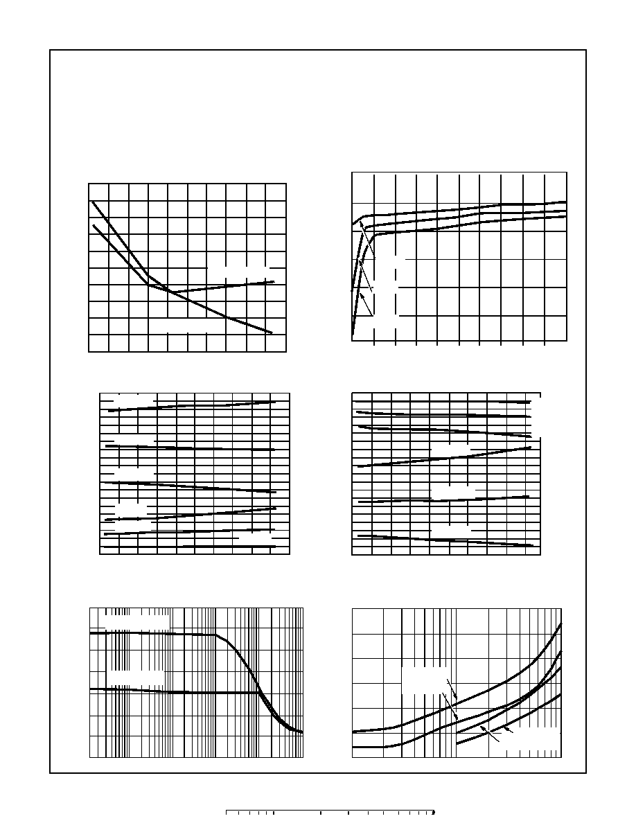
DESIGN INFORMATION
(Continued)
The information contained in this section has been developed through characterization by Intersil Corporation and is for use as application
and design information only. No guarantee is implied.
253
HA-2850
PSRR vs FREQUENCY
INPUT NOISE vs FREQUENCY
SLEW RATE vs TEMPERATURE
SLEW RATE vs SUPPLY VOLTAGE
Typical Performance Curves
V
SUPPLY
=
±
15V, A
V
= +10, R
L
= 1k
, C
L
10pF, T
A
= +25
o
C, Unless Otherwise Specified
(Continued)
100
10K
100K
1M
10M
FREQUENCY (Hz)
1K
100
90
80
70
60
50
40
30
20
10
0
110
P
S
RR (
d
B)
±
PSRR
60
50
40
30
20
10
0
N
O
I
S
E V
O
L
T
A
G
E (
n
V/
Hz
)
10
100
1K
10K
100K
NOISE CURRENT
NOISE VOLTAGE
FREQUENCY (Hz)
60
50
40
30
20
10
0
NO
IS
E
CURRE
NT
(
p
A/
Hz
)
350
325
300
275
250
S
L
EW
R
A
T
E (
V
/
µ
s)
-60
-40
-20
0
+20
+40
+60
+80 +100 +120 +140
TEMPERATURE (
o
C)
225
325
300
275
250
225
SL
EW
R
A
T
E (
V
/
µ
s)
5
6
7
8
9
10
11
12
13
14
15
SUPPLY VOLTAGE (
±
V)
350
Spec Number
511095-883
DESIGN INFORMATION
(Continued)
The information contained in this section has been developed through characterization by Intersil Corporation and is for use as application
and design information only. No guarantee is implied.
254
HA-2850
INPUT OFFSET VOLTAGE AND INPUT BIAS CURRENT vs
TEMPERATURE
SUPPLY CURRENT vs SUPPLY VOLTAGE
POSITIVE OUTPUT SWING vs TEMPERATURE
NEGATIVE OUTPUT SWING vs TEMPERATURE
MAXIMUM UNDISTORTED OUTPUT SWING vs FREQUENCY
TOTAL HARMONIC DISTORTION vs FREQUENCY
Typical Performance Curves
V
SUPPLY
=
±
15V, A
V
= +10, R
L
= 1k
, C
L
10pF, T
A
= +25
o
C, Unless Otherwise Specified
(Continued)
6.5
6.0
5.5
5.0
4.5
4.0
-60
-40
-20
0
+20 +40 +60 +80 +100 +120 +140
3.5
2.5
1.5
0.5
-0.5
I
N
P
U
T
O
F
F
S
E
T
VO
L
T
A
G
E
(
m
V)
BIAS CURRENT
OFFSET VOLTAGE
TEMPERATURE (
o
C)
INP
U
T
BIAS
CURRE
NT
(
µ
A)
8.0
7.5
7.0
6.5
6.0
5.5
5.0
S
U
P
P
L
Y
CURRE
NT
(
m
A)
5
6
7
8
9
10
11
12
13
14
15
SUPPLY VOLTAGE (
±
V)
+125
o
C
+25
o
C
-55
o
C
13
9
5
PO
SI
T
I
V
E
O
U
T
P
U
T
S
W
I
N
G
(
V
)
-60
-40 -20
0
+20 +40 +60 +80 +100 +120 +140
TEMPERATURE (
o
C)
3
7
11
±
8V, 75
±
15V, 1k
±
15V, 150
±
8V, 1k
±
8V, 150
±
15V, 75
-60
-40 -20
0
+20 +40 +60 +80 +100 +120 +140
TEMPERATURE (
o
C)
N
E
GA
T
I
V
E
OU
T
P
U
T
S
W
I
N
G
(
V
)
-3
-7
-11
-13
-5
-9
±
8V, 75
±
8V, 150
±
8V, 1k
±
15V, 75
±
15V, 1k
±
15V, 150
30
25
20
15
10
5
0
O
U
TP
U
T
V
O
LTA
G
E
S
W
I
N
G
(V
P-
P
)
1K
10K
100K
1M
10M
100M
FREQUENCY (Hz)
V
SUPPLY
=
±
8V
V
SUPPLY
=
±
15V
100K
1M
10M
-40
-50
-60
-70
-80
-90
FREQUENCY (Hz)
V
O
= 2V
P-P
V
O
= 0.5V
P-P
V
O
= 1V
P-P
T
HD (
d
Bc
)
-30
V
O
= 10V
P-P
-30
Spec Number
511095-883
255
All Intersil U.S. products are manufactured, assembled and tested utilizing ISO9000 quality systems.
Intersil Corporation's quality certifications can be viewed at www.intersil.com/design/quality
Intersil products are sold by description only. Intersil Corporation reserves the right to make changes in circuit design, software and/or specifications at any time without
notice. Accordingly, the reader is cautioned to verify that data sheets are current before placing orders. Information furnished by Intersil is believed to be accurate and
reliable. However, no responsibility is assumed by Intersil or its subsidiaries for its use; nor for any infringements of patents or other rights of third parties which may result
from its use. No license is granted by implication or otherwise under any patent or patent rights of Intersil or its subsidiaries.
For information regarding Intersil Corporation and its products, see www.intersil.com
HA-2850
TYPICAL PERFORMANCE CHARACTERISTICS
Device Characterized at: V
SUPPLY
=
±
15V, R
L
= 1k
, C
L
10pF, Unless Otherwise Specified
PARAMETERS
CONDITIONS
TEMPERATURE
TYPICAL
UNITS
Input Offset Voltage
V
CM
= 0V
+25
o
C
0.6
mV
Full
2.0
mV
Average Offset Voltage Drift
Versus Temperature
Full
20
µ
V/
o
C
Input Bias Current
V
CM
= 0V
+25
o
C
5.0
µ
A
Full
8.0
µ
A
Input Offset Current
V
CM
= 0V
+25
o
C
1.0
µ
A
Differential Input Resistance
+25
o
C
10
k
Input Noise Voltage Density
f
O
= 1000Hz
+25
o
C
11
nV
/
Hz
Input Noise Current Density
f
O
= 1000Hz
+25
o
C
6.0
pA
/
Hz
Large Signal Voltage Gain
V
OUT
=
±
10V
+25
o
C
25
kV/V
Full
20
kV/V
CMRR
V
CM
=
±
10V
Full
80
dB
Gain Bandwidth Product
+25
o
C
470
MHz
Output Voltage Swing
R
L
= 1k
Full
±
11
V
Output Current
V
OUT
10V
Full
±
20
mA
Output Resistance
Open Loop
+25
o
C
30
Full Power Bandwidth
FPBW = SR/2
V
P
, V
P
= 10V
+25
o
C
5.4
MHz
Slew Rate
V
OUT
=
±
10V, A
V
= +10
+25
o
C
340
V/
µ
s
Rise and Fall Time
V
OUT
=
±
100mV, A
V
= +10
+25
o
C
5
ns
Overshoot
V
OUT
=
±
100mV, A
V
= +10
+25
o
C
25
%
PSRR
Delta V
S
=
±
10V to
±
20V
Full
90
dB
Supply Current
No Load
Full
7.5
mA
Differential Gain
A
V
= +10, NTSC
+25
o
C
0.04
%
Differential Phase
A
V
= +10, NTSC
+25
o
C
0.04
Degrees
Harmonic Distortion
A
V
= +10, f = 1MHz, V
OUT
= 2V
P-P
+25
o
C
-74
dBc
Spec Number
511095-883